


Fabrication of CoFe2 O4 ferrite nanowire arrays in porous silicon template and their local magnetic properties
[Zheng Hui, Han Man-Gui†,  , Deng Long-Jiang]
, Deng Long-Jiang]
|
|


† Corresponding author. E-mail:
Project supported by the National Natural Science Foundation of China (Grant No. 61271039), the Scientific Projects of Sichuan Province, China (Grant No. 2015HH0016), and the Natural Science Foundations of Zhejiang Province, China (Grant Nos. LQ12E02001 and Y107255).
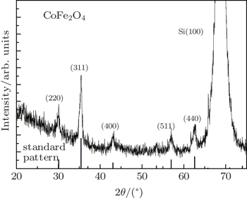
CoFe2O4 ferrite nanowire arrays are fabricated in porous silicon templates. The porous silicon templates are prepared via metal-assisted chemical etching with gold (Au) nanoparticles as the catalyst. Subsequently, CoFe2O4 ferrite nanowires are successfully synthesized into porous silicon templates by the sol–gel method. The magnetic hysteresis loop of nanowire array shows an isotropic feature of magnetic properties. The coercivity and squareness ratio (Mr/Ms) of ensemble nanowires are found to be 630 Oe (1 Oe, = 79.5775 A·m−1 and 0.4 respectively. However, the first-order reversal curve (FORC) is adopted to reveal the probability density function of local magnetostatic properties (i.e., interwire interaction field and coercivity). The FORC diagram shows an obvious distribution feature for interaction field and coercivity. The local coercivity with a value of about 1000 Oe is found to have the highest probability.
Recently, one-dimensional (1D) magnetic structures, especially magnetic nanowire arrays, have attracted much attention due to their unique potential applications in magnetic integrated nanosystems, perpendicular magnetic records, microwave absorbing and spintronic nanodevices.[1–4] Cobalt spinel ferrite CoFe2O4 (CFO) is well known for its high coercivity, giant magnetostriction, unique light-induced coercivity change, and remarkable chemical stability. CFO has various applications, such as humidity sensors, photodetectors, biomedical, magnetoelectric devices.[5–7] Lately, it was reported that magnetic nanowires can be fabricated by many approaches such as electrospinning, sol–gel, hydrothermal and electrodeposition methods.[8–10] Pirouzfar et al. have synthesized CFO nanowires with high coercivity values via the sol–gel route by using anodized aluminum oxide (AAO) as template.[9] Besides, Xu et al. have fabricated CFO nanowires with the preferred crystalline orientation along the length direction of nanowires by electrodeposition in AAO templates.[10] As shown in these studies, most CFO nanowire arrays or other ferrite nanowire arrays were fabricated in AAO templates.[11,12] However, the AAO templates are very fragile and easy to break into pieces, which are required to be handled with special caution. Therefore, it makes them extreme difficult to be assembled into sturdy devices. Currently, there is a trend towards incorporating many functions into silicon substrates, such as systems on chips.[4,13] Therefore, it is very important to be capable of fabricating CFO nanowire array in silicon, which will be compatible with semiconductor industry in future for the integrated nanosystems. In this paper, we report the fabrication of CFO nanowire array on silicon substrate and its magnetic properties. To the best of our knowledge, no one else has done this before. Since porous silicon was discovered,[14] it has attracted lots of attention due to its potential applications in optoelectronics, chemical and biochemical sensing devices.[15,16] Usually, porous Si is prepared by electrochemical etching under anodic bias in fluoride-containing solutions.[17] Recently, a new method based on metal-assisted chemical etching has attracted increasing attention for its simplified and low-cost fabricating process.[18,19] In this paper, we first prepare the porous silicon templates by a technique named metal-assisted chemical etching through using Au nanoparticles as the catalysts. Then the CFO nanowire arrays are fabricated into the channel of porous silicon by the sol–gel method. The local magnetic properties of CFO nanowire arrays have been investigated by taking the first order reversal curve (FORC). The conventional magnetic hysteresis loop taken by a conventional magnetometry, such as vibrating sample magnetometry (VSM), usually shows the ensemble average properties over a whole sample. Especially there are more than millions of nanoscale elements in a nanodot (or nanowire) array, and the variations of magnetic properties of individual elements (such as coercivity, switching fields) are essentially important. Using the FORC method, much meaningful information about these variations can be obtained such as the distribution of magnetic properties, the quantitative phase analysis of mixed magnetic phases materials and distinguishing the reversible and irreversible magnetization switching processes.[20–23]
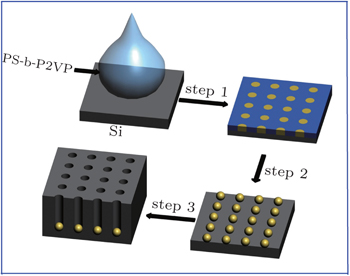
Single crystalline p-type silicon (200 Ω·cm) wafers were successively washed by immersing into acetone for 10 min, ethyl alcohol for 10 min and 5% HF for 5 min, which can remove the organic contaminants and a thin silicon dioxide layer. Polystyrene-block-poly(2-vinylpyridine) (PS-b-P2VP) diblock copolymer (Mn,NMR = 1.2× 10⁴ g/mol, PS20-b-P2VP190) was synthesized in our laboratory, and it was dissolved in toluene to form a 5-mg/ml solution. Subsequently, the experiments were carried out in three steps, which were schematically shown in Fig.
 | Fig. 1. Schematic procedures of preparation of porous silicon template. |
Metal nitrates were used as the cationic sources, and citric acid and polyethylene glycol (PEG 20000) as the monomers for forming the polymeric matrix. Citric acid and PEG were dissolved in deionized water by stirring at 80 °C to make the first solution. Co(NO3)2·6H2O and Fe(NO3)3·9H2O were dissolved in deionized water with a molar ratio of 1:2, and then mixed with the first solution. The molar ratio of total nitrates to citric acid was 1:1. The weight ratio of CoFe2O4 to PEG was 1:2. The final solution was stirred at 80 °C for 3 h to induce esterification and form a sol. The porous Si template was immersed in this sol with the aid of ultra sound. The sol in the porous Si template was dried in air at 80 °C for 1 h. Excess sol on the template surface was carefully wiped off and then was sintered in a furnace at 800 °C for 1 h.
The morphologies of Au nanoparticles, CoFe2O4 nanowire, surface, and cross section of porous Si template were investigated by a scanning electron microscope (SEM). The composition of CFO nanowires was checked by an energy dispersive spectrometer (EDS). The phase of nanowires was examined by x-ray diffraction (Cu Kα radiation). The static magnetic properties were investigated by a vibrating sample magnetometer (VSM). Using the conventional VSM, the FORC method requires to take a series of partial hysteresis curves (FORC curves), which fill the interior of a major hysteresis loop of sample. For each FORC curve, the sample was firstly saturated at a large positive field (Hs). Subsequently, the applied field was reduced to a reversal field (Ha), the sample was saturated again starting from Ha. The magnetization of each applied field (Hb) on the FORC curve is denoted as M(Ha, Hb). For a set of FORC measurements, it must be noted that the field spacing should be equal (i.e., ΔHb = ΔHa). According to the statistical model (called “Preisach model”) which describes a set of hysterons that constitute a major hysteresis loop, the probability density function ρ (Ha,Hb) (also called FORC distribution) of the hysterons ensemble can be calculated by the following mixed second derivative:

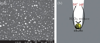
PS-b-P2VP consists of a nonpolar PS block covalently linked to a polar P2VP domain. It spontaneously forms a monodisperse PS corona and P2VP core micelles in toluene which is a selective solvent for the PS block and nonselective solvent for P2VP. When it is coated by spin coating onto the clean silicon wafer with a rotation speed of 5000 rpm, the polymer molecules are self-assembled into a thin film with P2VP nano domains surrounded by PS corona.[24] Once the PS-b-P2VP thin film is immersed into HAuCl4 solution with methanol (a selective solvent for the P2VP core), core-corona inversion is induced in-situ without ruining the film.[25] The HAuCl4 is then loaded into the P2VP due to the pyridine complexing reaction.[26] Subsequently, the Au nanoparticles can be obtained by reducing the HAuCl4 solution in the sodium citrate solution. Finally, the polymer layer is removed with an alcohol lamp without disturbing the nanoparticle pattern.[27,28] In our experiments, the arrangement of Au nanoparticles on the silicon surface is shown in Fig.
 | Fig. 2. (a) Arrangement of Au nanoparticles on the surface of silicon template, and (b) mechanism of porous silicon preparation by metal assisted chemical etching. |
After the array of Au nanoparticles is obtained, the silicon template with the surface modified by Au is immersed into an aqueous solution containing HF and H2O2. The mechanism of the Au-assisted chemical etching is illustrated in Fig.


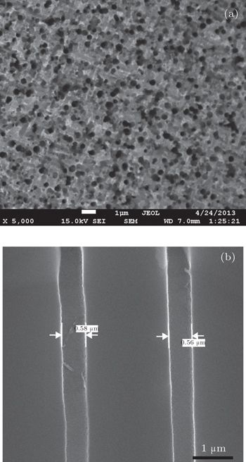
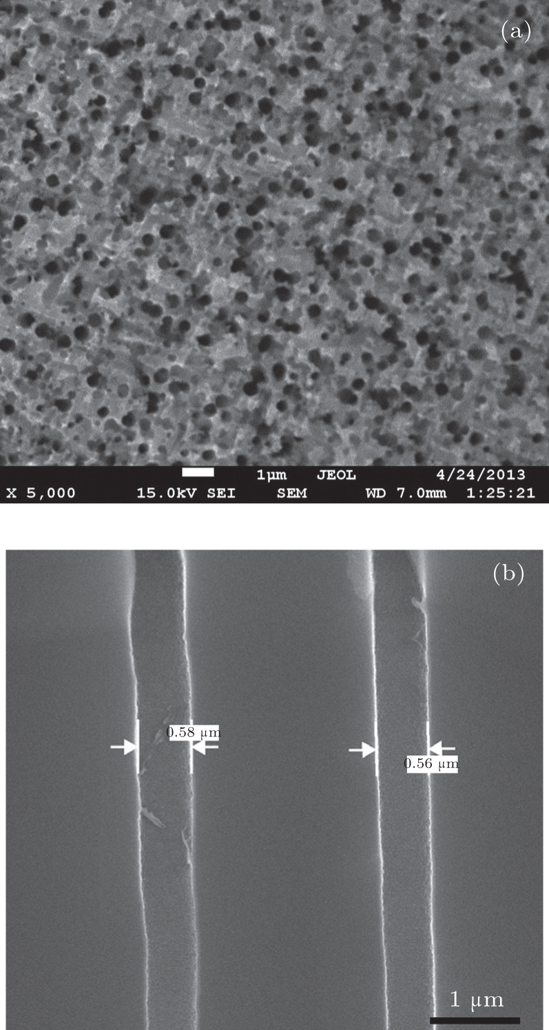 | Fig. 3. SEM images of (a) top view and (b) cross section view of porous silicon template. |
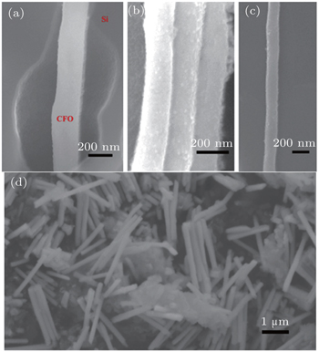
The CFO nanowires are shown in Figs.
 | Fig. 4. (a)–(d) SEM images of CoFe2O4 nanowires. |
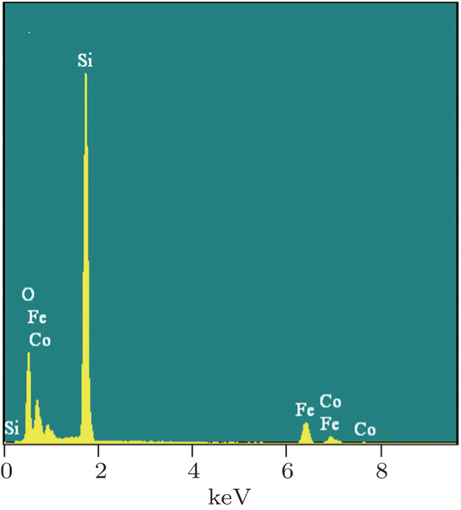 | Fig. 5. Composition analysis of CoFe2O4 nanowire array. |
 | Fig. 6. XRD pattern of CoFe2O4 nanowires array. |
The static magnetic properties of CFO nanowires in porous templates are studied by using the hysteresis loops as shown in Fig.
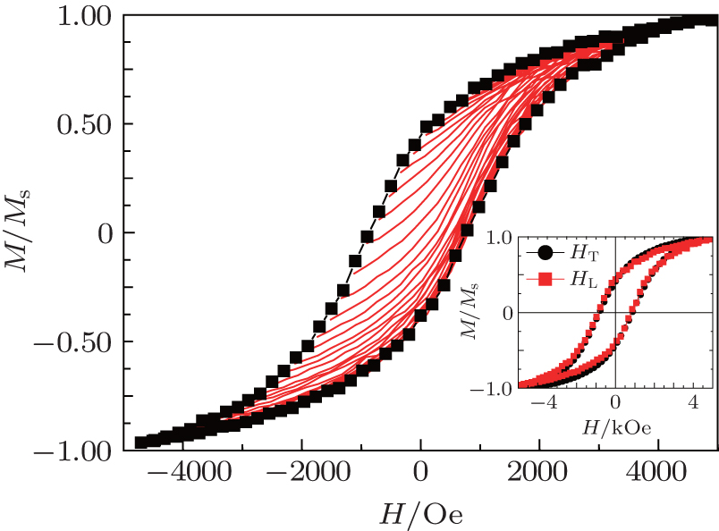 | Fig. 7. First order reversal curves of CoFe2O4 nanowire arrays. Hysteresis loops in the inset are measurements in two different directions of applied field. |
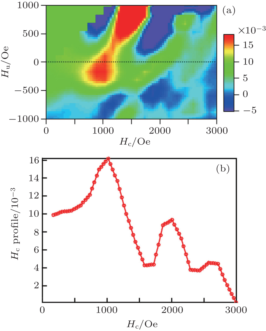 | Fig. 8. (a) FORC diagrams of CoFe2O4 array, and (b) coercivity profile. |
In this study, cobalt spinel ferrite nanowires are synthesized by a sol–gel method into the porous silicon template which is fabricated by the Au-assisted chemical etching procedure. It is found that the pore size is dependent on the size of Au nanoparticle. The spacing between nanopores is dependent on the spacing between Au nanoparticles on silicon substrate. For the ensemble CFO nanowires, conventional hysteresis loops show that the magnetic properties of CFO nanowire array in porous silicon template are isotropic. However, the FORC diagram derived from a series of first order reversal curves shows the wide distributions of local magnetic properties (Hu and Hc). For instance, the local coercivity with a value of about 1000 Oe is found to have the highest probability. The inhomogeneity of pore sizes and pore spacings is one of the causes responsible for the distribution of local magnetic properties.
| 1 | |
| 2 | |
| 3 | |
| 4 | |
| 5 | |
| 6 | |
| 7 | |
| 8 | |
| 9 | |
| 10 | |
| 11 | |
| 12 | |
| 13 | |
| 14 | |
| 15 | |
| 16 | |
| 17 | |
| 18 | |
| 19 | |
| 20 | |
| 21 | |
| 22 | |
| 23 | |
| 24 | |
| 25 | |
| 26 | |
| 27 | |
| 28 | |
| 29 | |
| 30 | |
| 31 |