Tuning the energy gap of bilayer α-graphyne by applying strain and electric field
[Hang Yang, Wen-Zhi Wu, Yu Jin, Guo Wan-Lin†,  ]
]
]
|
|


† Corresponding author. E-mail:
Project supported by the National Key Basic Research Program of China (Grant Nos. 2013CB932604 and 2012CB933403), the National Natural Science Foundation of China (Grant Nos. 51472117 and 51535005), the Research Fund of State Key Laboratory of Mechanics and Control of Mechanical Structures, China (Grant No. 0414K01), the Nanjing University of Aeronautics and Astronautics (NUAA) Fundamental Research Funds, China (Grant No. NP2015203), and the Priority Academic Program Development of Jiangsu Higher Education Institutions.
Our density functional theory calculations show that the energy gap of bilayer α-graphyne can be modulated by a vertically applied electric field and interlayer strain. Like bilayer graphene, the bilayer α-graphyne has electronic properties that are hardly changed under purely mechanical strain, while an external electric field can open the gap up to 120 meV. It is of special interest that compressive strain can further enlarge the field induced gap up to 160 meV, while tensile strain reduces the gap. We attribute the gap variation to the novel interlayer charge redistribution between bilayer α-graphynes. These findings shed light on the modulation of Dirac cone structures and potential applications of graphyne in mechanical-electric devices.
Graphyne,[1–3] an sp- and sp2-hybridized carbon allotrope predicted by Baughman et al.,[1] has become a new topic in two-dimensional (2D) materials since Li et al.[3] and Liu et al.[4] reported the successful preparation of the large area graphdiyne film by a cross-coupling reaction using hexaethynylbenzene. Besides, lots of theoretical research has been reported on the mechanical stability[5–8] and electronic properties[9–12] of graphyne as well as its derivates. Previous first-principle calculations[9,13–15] have shown that α-, β-, and 6,6,12-graphyne possess the graphene-like Dirac cone band structures around the Fermi surface and they also exhibit small carrier effective mass values and high carrier mobilities like those of graphene. However, like graphene,[16] it brings the same problem that pristine graphyne in the above cannot be used to build logical circuits with low power consumption at room temperature because it is a zero-gap semimetal. Bilayer stacking is a good choice to solve this problem since it can achieve the controllable semimetal to semiconductor transition under an external electric field.[17–23] But the band modulation in bilayer graphyne has never been clearly clarified yet.
In this paper, based on first-principle calculations, we show how the electronic structure of bilayer α-graphyne is tuned by a perpendicular electric field and interlayer strain. Our results show that bilayer α-graphyne opens a gap under external electric field, which is consistent with the result in previous work.[21] Though bilayer α-graphyne keeps the semimetal properties under interlayer strain, the field-induced gap can be modulated by interlayer strain over a wide range, which limitation exhibits a great increase with the decrease of interlayer distance. These results show that the combination of interlayer strain and electric field is an efficient method to tune the electronic structure of bilayer α-graphyne.
All calculations were performed using the VASP code[24,25] with the Perdew–Burke–Ernzerhof (PBE) pseudo-potential[26] and generalized gradient approximation (GGA) for the exchange–correlation potential. The projector augmented wave method (PAW)[27] was applied with an energy cutoff of 500 eV for the plane wave basis. A gamma-centered 12 × 12 × 1 k-point sampling was used for the Brillouin-zone integration and a vacuum region larger than 15 Å was used to eliminate the interaction between the neighboring slabs. All the ionic coordinates were fully optimized until the forces were less than 0.01 eV/Å. Given the long-range vdW interaction, we employed the optB86b-vdW method[28,29] to generate accurate equilibrium interatomic distance and energy. The external electric field was introduced by planar dipole layer method along the direction perpendicular to the graphyne planes.[30]
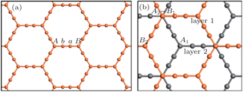
We first discuss the structure and stability of bilayer α-graphyne. As shown in Fig.
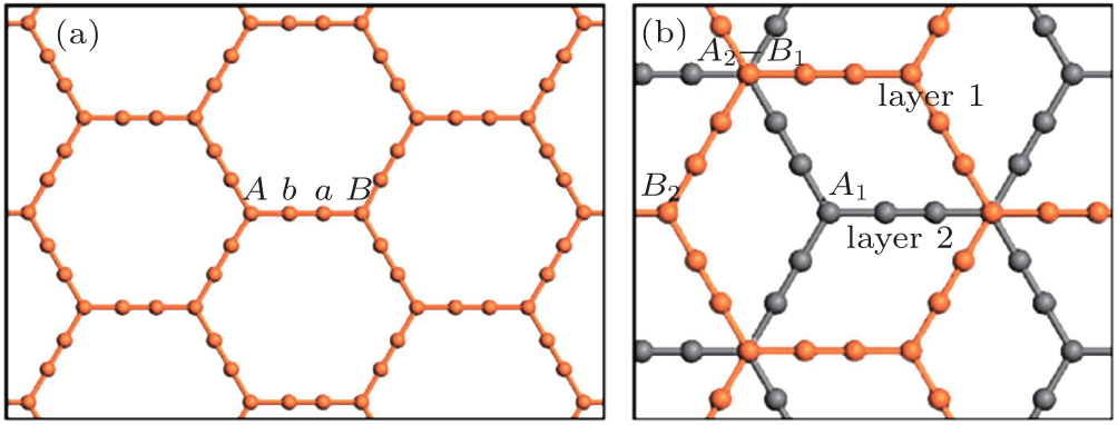 | Fig. 1. (a) Geometric structure of single-layer α-graphyne and (b) bilayer α-graphyne with AB stacking. The inequivalent atoms are indicated and different layers are shown in different colors. |
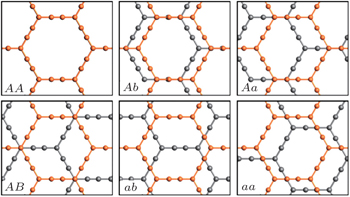
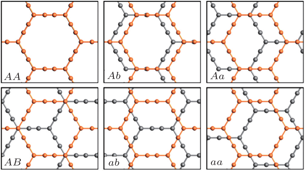 | Fig. S1. Geometry structures of bilayer α-graphyne with six inequivalent stacking modes. Different layers are shown in different colors. |
| Table S1. Values of interlayer distance d and binding energy E of bilayer graphyne with six inequivalent stacking modes. . |
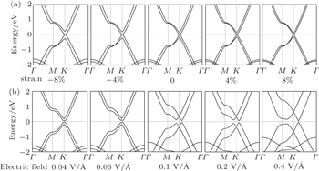
Strain is usually used to modulate the electronic properties in a 2D system.[31–33] Specifically, strain has been widely predicted to modulate the band structure in bilayer graphene and bring graphene into practical application.[17–20] Hence, it is of both fundamental and practical interest to examine the effect of interlayer strain on the electronic properties of bilayer α-graphyne. The interfacial strain is simulated by changing the interlayer distance between the two graphyne layers. The calculated band structures of bilayer graphyne with different interlayer distances are shown in Fig.
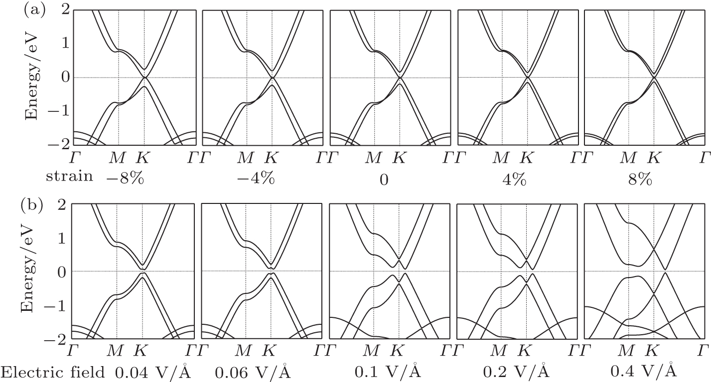 | Fig. 2. (a) A series of band structures of bilayer graphyne under strains of ±8%, ±4%, and 0, without external electric fields. (b) Band structures of strain-free bilayer graphyne under electric fields of 0.04, 0.06, 0.1, 0.2, and 0.4 V/Å. |
Next, we explore the electronic properties of bilayer graphyne under a vertical electric field Eext. The band structures of bilayer graphyne under various fields are shown in Fig.
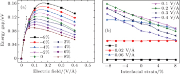
As mentioned above, interlayer strain cannot open the gap of bilayer graphyne, but it plays an important role in the interlayer coupling in bilayer graphyne. Given that both strain and electric field are feasible tools in tuning the electronic properties of materials in actual device designing, it should be interesting to investigate their combined effect. Here in this work, we demonstrate the important role of strain played in the electronic properties of bilayer graphyne under electric field. The energy gap variations with electric field and interlayer strain are shown in Fig.
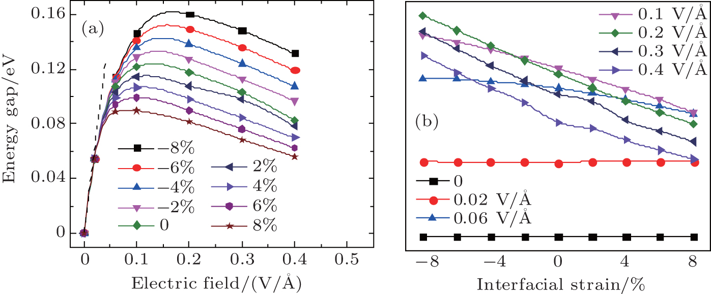 | Fig. 3. (a) Variations of the energy gap with electric field under different strains. The dashed line on the left of the curves indicates the linearly increasing gap with a slope of 0.272 eV per V/Å. (b) Variations of the energy gap with the interlayer strain at different electric fields. |
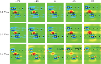
To further study the mechanism of the strained bilayer graphyne under external electric field, we plot the charge density difference (

 | Fig. 4. Projections of the charge density difference to the {100} surface under strains of ± 8%, ± 4%, and zero in the fields of 0.1, 0.2, and 0.4 V/Å. The value and location of the largest charge density difference (in units of e/Å3) are shown in each panel. |
In this work, we systematically investigate the electronic properties of bilayer α-graphyne under interlayer strain and electric field by first-principle calculations. The combined effect of strain and electric field can efficiently modulate the energy gap of the bilayer structure over a wide range of interlayer distance and electric field, which stems from the novel interlayer charge redistribution. The tunable energy gap in bilayer α-graphyne provides robust and viable applications in the future mechanical-electric devices.
| 1 | |
| 2 | |
| 3 | |
| 4 | |
| 5 | |
| 6 | |
| 7 | |
| 8 | |
| 9 | |
| 10 | |
| 11 | |
| 12 | |
| 13 | |
| 14 | |
| 15 | |
| 16 | |
| 17 | |
| 18 | |
| 19 | |
| 20 | |
| 21 | |
| 22 | |
| 23 | |
| 24 | |
| 25 | |
| 26 | |
| 27 | |
| 28 | |
| 29 | |
| 30 | |
| 31 | |
| 32 | |
| 33 | |
| 34 |