


Characterization of vertical Au/ β -Ga 2 O 3 single-crystal Schottky photodiodes with MBE-grown high-resistivity epitaxial layer
[Liu X Z 1, †,  , Yue C 1 , Xia C T 2, ‡, , Zhang W L 1 ]
, Yue C 1 , Xia C T 2, ‡, , Zhang W L 1 ]
|
|


† Corresponding author. E-mail:
‡ Corresponding author. E-mail:
Project supported by the National Nature Science Foundation of China (Grant No. 61223002) the Science and Technology Commission of Shanghai Municipality, China (Grant No. 13111103700), and the Specialized Research Fund for the Doctoral Program of Higher Education of China (Grant No. 2012018530003).
High-resistivity β -Ga 2 O 3 thin films were grown on Si-doped n-type conductive β -Ga 2 O 3 single crystals by molecular beam epitaxy (MBE). Vertical-type Schottky diodes were fabricated, and the electrical properties of the Schottky diodes were studied in this letter. The ideality factor and the series resistance of the Schottky diodes were estimated to be about 1.4 and 4.6× 10 6 Ω. The ionized donor concentration and the spreading voltage in the Schottky diodes region are about 4 × 10 18 cm −3 and 7.6 V, respectively. The ultra-violet (UV) photo-sensitivity of the Schottky diodes was demonstrated by a low-pressure mercury lamp illumination. A photoresponsivity of 1.8 A/W and an external quantum efficiency of 8.7 × 10 2 % were observed at forward bias voltage of 3.8 V, the proper driving voltage of read-out integrated circuit for UV camera. The gain of the Schottky diode was attributed to the existence of a potential barrier in the i–n junction between the MBE-grown highly resistive β -Ga 2 O 3 thin films and the n-type conductive β -Ga 2 O 3 single-crystal substrate.
The unique properties of gallium oxide with β -type crystal structure ( β -Ga 2 O 3 ) stimulated the study of growth and characteristics of that material in view of new applications. After large-size high-quality melt-grown gallium oxide single-crystal wafers were successfully manufactured, β -Ga 2 O 3 has attracted increasing interest as a promising wide band gap semiconductor. [ 1 ] β -Ga 2 O 3 has a wide band gap of about 4.8 eV, the widest among other oxide semiconductors, such as ZnO (3.4 eV) and SnO 2 (3.6 eV), [ 2 , 3 ] paves the way to deep ultraviolet (DUV) optical applications. [ 4 ] In particular, photodetectors with solar-blind sensitivity have attracted significant attention, because they respond only to DUV light, even under sun and room illuminations, which is very suitable for monitoring ozone holes and detecting flames.
In order to develop solar-blind photodetectors, a lot of research work based on β -Ga 2 O 3 thin films has been demonstrated. [ 5 , 6 ] However, all the films were polycrystalline because of the unique crystal structure of β -Ga 2 O 3 , which lacks a suitable heteroepitaxial substrate. The crystalline quality of β -Ga 2 O 3 thin films is assumed for direct relationships with photoresponsivity of the photodetectors. The grain boundaries of the polycrystalline thin films act as traps for photogenerated carriers, which results in a long response time. Other than thin-film photodetectors, in order to get a short response time, β -Ga 2 O 3 nanostructure photodetectors were reported. [ 7 , 8 ] Better crystalline quality of the β -Ga 2 O 3 nanowires and nanobelts resulted in a fast photo-response. However, the fabrication process of nanowire-based device array is still an area in progress. Therefore, to fully develop the potential application of β -Ga 2 O 3 , photodetectors based on single crystals are needed.
Recently, β -Ga 2 O 3 single crystals have become available. [ 9 , 10 ] For vertical-type photodetectors, Schottky contacts and ohmic contacts were formed on the surface and on the back side of the single crystal substrate, respectively. In order to reduce the dark current of the photo-diode, a high resistive layer was usually introduced to form a metal–insulator–semiconductor (MIS) configuration instead of the metal–semiconductor (MS) configuration. Oshima et al . fabricated a vertical-type Schottky photo-detector based on undoped n-type β -Ga 2 O 3 single crystal. [ 11 ] In order to introduce a high resistive layer, the β -Ga 2 O 3 single crystal was thermally annealed at 1100 °C for 6 h in ambient oxygen to reduce the oxygen vacancies and decrease the carrier concentration near the surface. Suzuki et al . demonstrated an MIS photodiode by sol–gel depositing a high-resistivity β -Ga 2 O 3 epitaxial layers on undoped n-type β -Ga 2 O 3 single crystal substrates. [ 12 ]
Besides the crystalline quality of β -Ga 2 O 3 epitaxial layers, presence of donor and acceptor defects, providing successively free electrons and holes, are believed for their direct relationships with photoresponsivity of β -Ga 2 O 3 ultra-violet (UV) detectors. [ 13 , 14 ] Molecular beam epitaxy (MBE) is well known to reduce the film impurity levels due to an ultrahigh vacuum environment and high purity source materials. Reproducible doping control and lower unintentional impurity levels in the epitaxial films are achievable by using plasma-assisted molecular-beam-epitaxy (PAMBE). [ 15 , 16 ] In this paper, vertical-type Schottky photodiodes were fabricated by PAMBE growing high resistivity β -Ga 2 O 3 thin films on the highly conductive Si-doped β -Ga 2 O 3 single crystals. The electrical properties of the photodiodes are analyzed.
Double-side polished (100) β -Ga 2 O 3 single crystal substrates used in this study were fabricated from an Si-doped single crystal ingot grown by the floating zone method. [ 10 ] The Si-doped single crystal ingot was an n-type semiconductor with a resistivity of about 9 × 10 3 Ω·cm at room temperature. The (100) β -Ga 2 O 3 single-crystal substrates were about 0.5 mm in thickness. Before high-resistivity homo-epitaxial layer growth, the substrates were cleaned with acetone and methanol.
The β -Ga 2 O 3 epitaxial layers were grown in an SVT PAMBE system. A standard shuttered Knudsen cell was used to evaporate gallium (99.9999%) and a mono-atomic oxygen from research-grade oxygen gas (99.998%) was supplied from a radio-frequency (RF) radical cell. The substrates were baked in the growth chamber at 650 °C for 30 min. Oxygen plasma treatment using a pressure of 1 × 10 −5 Torr at 650 °C for 30 min was conducted to remove the adsorbates from the substrate surface. On the basis of previous experiments of growth parameters optimization, the oxygen gas flow rate, the input RF power of radical cell, and the temperature of K-cell were maintained at 1 sccm, 300 W, and 940 °C, respectively. An optimized substrate temperature of 760 °C was chosen, and the growth rate was about 50 nm/h. The growth time was fixed at 2 h for all samples, resulting in the gallium oxide layers with thicknesses of about 100 nm as characterized by surface profiler and cross-sectional scanning electron microscopy.
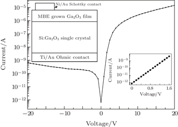
To fabricate a photodiode, a large area of square Ti/Au (∼ 40 nm/240 nm) Ohmic contact (5 mm×5 mm) was first deposited on the back side of the n-type conductive substrate by electron-beam evaporation, and thermally annealed at 850 °C for 30 seconds in ambient nitrogen. The specific contact resistivity is about 3 × 10 −2 Ω·cm 2 . The contact resistance is about 0.12 Ω, which means good Ohmic characteristics of the Ti/Au electrode after annealing. Then 0.5 mm×0.5 mm square Au (5–10 nm) Schottky contacts were deposited on the surface of the MBE grown β -Ga 2 O 3 epitaxial layers through metal mask. The device configuration is illustrated in the insertion of Fig.
 | Fig. 1. I – V characteristics of the Schottoky diode. The insertion shows the cross-sectional schematic illustration of the Schottky diode and the I – V characteristics at low forward bias voltages. |
The current–voltage ( I – V ) characteristics of the photodiodes were measured with an HP-4155B semiconductor parameter analyzer. The capacitance of the photodiodes was characterized by a HP-4294A impedance analyzer. A low-pressure mercury lamp with a 254-nm line filters was used as UV light source to evaluate photo-responsivity. The incident light power was calibrated by using a calibrated UV-enhanced Si photodiode.
Figure
According to Cheung’s model, [ 17 ] the forward current–voltage ( I – V ) characteristics of a Schottky diode at low forward bias voltages can be expressed by
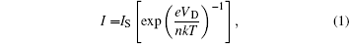
Because of the high resistivity layer in the fabricated diodes, the effect of the diode series resistance R s cannot be ignored. The voltage V D across the diode can then be expressed in terms of the total voltage drop V across the series resistor. Thus, V D = V – IR s . At room temperature, V D > 3 k B T / q is usually satisfied. Equation (


Thus, a plot of d V /d ln( I ) vs. I will give R s as the slope and n / β as the y -axis intercept. The R s parameter and the ideality factor of the fabricated Schottky diodes were estimated to be about 4.6 × 10 6 Ω and 1.4 as shown in Fig.
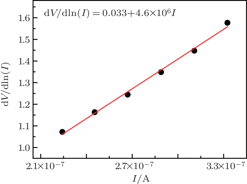 | Fig. 2. Plot of d V /d ln( I ) versus I of the Schottky diode. The insertion shows the linearly fitting result. |
Figure


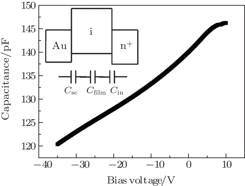 | Fig. 3. C – V characteristics of the Schottoky diode. The insertion shows the schematic illustration of band diagram and the equivalent circuit model of the Schottky diode. |
The saturation capacitance represents the capacitance of the highly resistive layer in series with the capacitance of the i–n junction,

Considering the continuity of the electric field at the interface between the highly resistive layer and the Schottky diode region, the following equations can be obtained: [ 18 ]


A plot of 


 | Fig. 4. Plot of  |
From Eqs. (
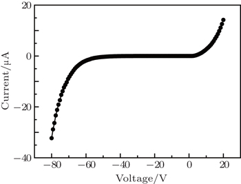
 | Fig. 5. The reverse breakdown characteristics of the Schottky diode. |
When the Schottky diode was irradiated by a low-pressure mercury lamp, a positive direction photo-current under forward bias in addition to a negative direction photo-current under reverse bias was observed. Figure
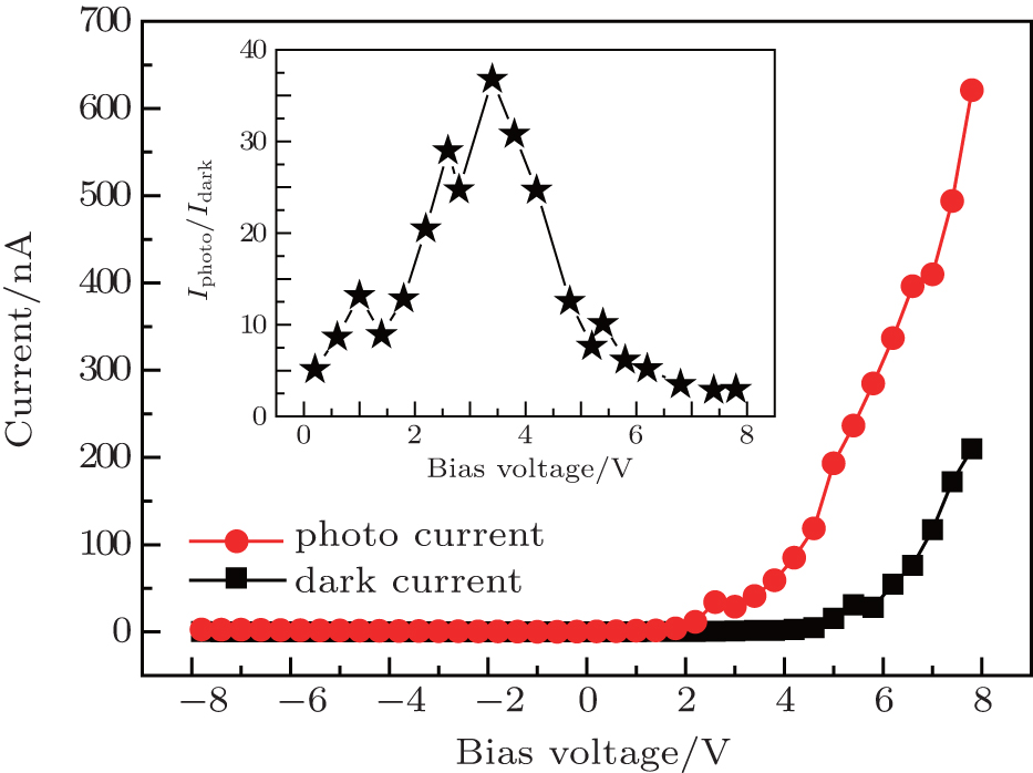 | Fig. 6. Dark current and photocurrent of the Schottky diode. The insertion shows the ratio of photocurrent to dark current of the Schottky diode. |
Highly-resistive β -Ga 2 O 3 epitaxial layers were grown on conductive Si-doped β -Ga 2 O 3 single-crystal substrates by the MBE. Vertical-type Schottky diodes with large photoresponsivity and external quantum efficiency were fabricated. A photoconductive device model with a potential barrier at the i–n junction was proposed to explain the gain of the Schottky diode.
| 1 | |
| 2 | |
| 3 | |
| 4 | |
| 5 | |
| 6 | |
| 7 | |
| 8 | |
| 9 | |
| 10 | |
| 11 | |
| 12 | |
| 13 | |
| 14 | |
| 15 | |
| 16 | |
| 17 | |
| 18 |