


Recovery of PMOSFET NBTI under different conditions
[Cao Yan-Rong†a), b)  , Yang Yi
a) , Cao Chenga) , He Wen-Longa) , Zheng Xue-Fengb) , Ma Xiao-Huac) , Hao Yueb) ]
, Yang Yi|
|

 , Yang Yi
†Corresponding author. E-mail: yrcao@mail.xidian.edu.cn
*Project supported by the National Basic Research Program of China (Grant No. 2011CBA00606), the National Natural Science Foundation of China (Grant Nos. 61404097, 61334002, 61106106, and 61176130), and the Fundamental Research Funds for the Central Universities, China (Grant No. JB140415).
Negative bias temperature instability (NBTI) has become a serious reliability issue, and the interface traps and oxide charges play an important role in the degradation process. In this paper, we study the recovery of NBTI systemically under different conditions in the P-type metal–oxide–semiconductor field effect transistor (PMOSFET), explain the various recovery phenomena, and find the possible processes of the recovery.
Negative bias temperature instability (NBTI) is a crucial reliability issue affecting the P-type metal– oxide– semiconductor field effect transistor (PMOSFET) with a negative voltage stress on the gate at high temperature.[1– 5] NBTI causes an increase of the threshold voltage Vth and a decrease of the drive current Id with time, and the parameters shift further at higher temperature and under stronger gate stress. In the conventional NBTI study, the device is stressed by a constant negative gate bias with its drain and source grounded.[6– 8] However, the NBTI degradation substantially recovers after the remove of the stress or under a smaller gate bias. Therefore, the conventional stress overestimates the degradation and underestimates the lifetime of the device.[9, 10] More attention has been paid to this problem in recent years.[11– 13] However, in spite of the intensive studies on the recovery issue, the physical mechanism is still far from being fully understood. In this paper, we study the recovery of NBTI systemically under different conditions in the 90-nm PMOSFETs, explain the various recovery phenomena, and find the possible processes of the recovery.
The PMOSFETs used here are of the surface channel. They were manufactured by using a 90-nm process technology and had lightly doped drain (LDD) structures and shallow trench isolation (STI) schemes. The devices were 0.1 μ m in length, 10 μ m in width, and 1.4 nm in oxide thickness. The gate oxides of all devices were annealed in N2O atmosphere after thermal growth. HP 4156B, a high precision semiconductor parameter analyzer, was used to complete the tests. The devices were stressed under NBTI stress conditions of Vg = Vstress and Vd = Vs = 0 at elevated temperatures for different cycles. The stress was interrupted at regular intervals, and the device parameters such as threshold voltage Vth were measured to monitor the degradation of the device. After the stress process, the recovery process was studied under different gate biases at different temperatures.
To study the recovery mechanism, experiments were carried out to obtain the results of different recovery processes under different gate biases at different temperatures. As the threshold voltage Vth is one of the most important parameters, the difference between the initial Vth indicated by Vth0 and Vth (Δ Vth) was measured at the stress intervals. The Vth degradation was studied and its mechanism was analyzed.
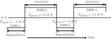
The applied alternating stress is shown in Fig. 1. The negative bias Vgstress = − 1.8 V is applied during the degradation process, and the positive bias Vgstress = + 1.8 V is applied during the recovery process. In order to study the recovery mechanism, the recovery process lasts 2000 s, while the degradation process lasts 1000 s. Suppose that the last Δ Vth of each negative bias stress cycle is 

 | Fig. 1. The applied alternating stress. |
In the NBTI degradation process, in addition to the interface trap generation, there are also generated H related species including H+ .[14] The H related species are easily trapped by the oxide traps during migrating to the gate. Furthermore, during the NBTI stress, a large number of inversion holes gather at the channel surface, and some of them can tunnel into the gate oxide and be trapped by the oxide traps. Therefore, when the negative gate stress is instantly removed, in addition to the H related species, there are also a number of positive charges in the oxide. The H related species and the positive charges can play a role in recovering NBTI. Figure 2 is the species distribution in the gate oxide under the NBTI stress.
 | Fig. 2. Relevant species distribution in the gate oxide in the NBTI degradation process. Here ⊕ represents positive charges trapped in the oxide, ◯ represents inversion holes. |
To study the recovery mechanism, we use a longer recovery time, and the variation of the threshold voltage under the applied alternating stress is shown in Fig. 3. We study the recovery and degradation stages in detail.
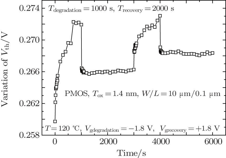 | Fig. 3. Time variation of threshold voltage under the alternating stress. |
The threshold voltage shifts of two recovery cycles are given in Fig. 4(a). The actual time range of the first recovery cycle is 1000– 3000 s, and that of the second recovery cycle is 4000– 6000 s. The markings are the degradation quantities of the degradation phases ahead of the two recovery cycles separately. As shown in Fig. 4, the recovery process can be divided into three stages: the stage marked by 1 is the first recovery stage, results from the detrapping of the oxide charges, and is the fast recovery stage; the stage marked by 2 is the second recovery stage due to the passivation of the interface traps by the H related species, and is the slow recovery stage; the stage marked by 3 is the third recovery stage and is the recovery saturation stage. In both the degradation and the recovery processes, there are H related species entering into the gate. Therefore, the H related species moving back and passivating the interface traps are reduced. The final recovery amount is smaller than the degradation, and the lock-in effect of part degradation or the recovery saturation stage comes out.[15]
 | Fig. 4. Recovery stages of NBTI: (a) the superposition of threshold voltage shifts of two recovery cycles, (b) the normalized superposition of the final threshold voltage degradation after recovery relative to that after the previous degradation process, (c) the normalized superposition of the threshold voltage recovery after the recovery stage relative to the final degradation after the previous degradation process, (d) the superposition of the threshold voltage recovery after the recovery stage to the real degradation of this cycle ratio. |
It is clear that the threshold voltage degradation after recovery of the second cycle is far larger than that of the first cycle. Mark the last points of the degradations as
The above results are all about degradation comparison between different cycles. Actually, the total degradation after the second cycle minus the final value of the first cycle is the real degradation during the second cycle. By comparing the ratio between the recovery after the recovery process and the real degradation of each cycle marked as Δ Vth– Degradation, we find that the recovery ratio of the second cycle is larger than that of the first cycle as shown in Fig. 4(d). Therefore, the reason why the final degradation of the recovery stage increases with cycle number increasing is not the decrease of recovery during each cycle, but the accumulation of recovery saturation during the recovery stage of each cycle.
From Fig. 4, we can clearly see that the final recovery is almost determined by the fast recovery stage. Namely, the detrapping of the gate oxide positive charges is the key. In addition, figure 4(d) shows that as the number of cycles increases, the effect of the detrapping of gate oxide positive charges is more significant.
The threshold voltage shifts of the two cycles in the NBTI degradation stress processes are shown in Fig. 5(a). The actual time range of the first degradation process is 0– 1000 s, and that of the second degradation process is 3000– 4000 s. On the whole, the degradation rate of the second process is far smaller than that of the first process. We consider the second degradation stage as an independent process, the threshold voltage shift relative to the end point of the first recovery stage is shown in Fig. 5(b). It is clear that the time exponent of the second stage is the same as that of the first stage, both stages meet the same degradation model, i.e., the H– H+ reaction diffusion model.[16]
 | Fig. 5. Two cycles of NBTI degradation stages: (a) the device threshold voltage shifts and (b) the normalized threshold voltage shifts. |
Figure 6 shows the recovery of the threshold voltage during the recovery stage at different temperatures. We can clearly see that the recovery decreases obviously when the temperature increases from 90 ° C to 150 ° C. This is because during the degradation of NBTI, the temperature plays an important role in the interfacial reaction and the reaction products’ diffusion to the gate oxide. Si– H bond breaking, which is a forward electrochemical reaction, is an endothermic process. The backward reaction, or the passivation reaction of the interface traps, is an exothermic process. The high temperature promotes the forward and the backward reactions to different degrees, disequilibrates the forward and the backward reactions, and relatively limits the passivation reaction rate. Hence, more H related species are produced with temperature rising. Meanwhile, the energy of the charged particle increases, which reduces the probability of the charged particles being trapped by the gate oxide traps. More H related species can enter into the ploy-Si gate, so the number of positive charges and that of the H related species which can diffuse back to the interface to passivate the interface traps become smaller. It eventually leads to the reduced device recovery at high temperature. Therefore, high temperature will solidify the damages of the gate oxide, shown as recovery saturation or a lock-in effect, which can enhance device damages.
 | Fig. 6. Normalized threshold voltage recovery at different temperatures. |
We can respectively obtain the recovery of the first and the second recovery stages from Fig. 6, corresponding to fast detrapping and passivation of the interface traps. Their relations to temperature are shown in Fig. 7. In the single logarithmic coordinate, they both show good linear relations with 1/KT and satisfy the equation

where R1 is the ratio between the normalized recovery Δ (recovery) and the initial degradation Δ 0, C is a constant, K is the Boltzmann constant, T is the absolute temperature, and 
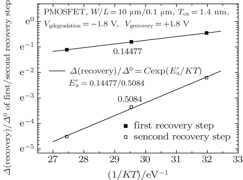 | Fig. 7. Variations of the first and the second recovery stage with temperature. |
Taking both recovery factors into account, we obtain the final device recovery as shown in Fig. 8. In the single logarithmic coordinate, the final recovery still shows an obvious linear relation with 1/KT and meets the following equation:

where R2 is the ratio between the normalized recovery quantity Δ Vth− Recovery and the initial degradation quantity 

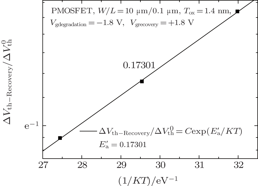 | Fig. 8. Dependence of total recovery on temperature during the recovery stage. |
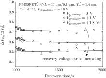
In the recovery process, the recovery of the NBTI effect differs under different recovery stress. Figure 9 shows the recovery of the threshold voltage under different gate biases. As shown in the figure, the recovery process can be divided into three stages and the recovery keeps increasing with the recovery stress varying from 0 V to 1.8 V. From the experimental results, we can obtain the reason why the recovery is mainly determined by the different fast recovery in the recovery stage. Higher recovery gate stress will lead to more gate oxide charges, which affects the device recovery. Besides, the high gate voltage can also facilitate the H+ ions to diffuse back to the Si/SiO2 interface to passivate the interface traps in a short time. So the larger fast recovery is produced.
 | Fig. 9. Normalized Vth recovery under different recovery gate biases. |
We extract the respective and the total amount of recovery, as shown in Fig. 10. It shows the obvious dependence of recovery after NBTI stress on the gate bias. All three kinds of recovery present good linear relations with the recovery gate bias. The total recovery meets the following equation:

where R is the ratio between normalized recovery Δ Vth− Recovery and the initial degradation

 | Fig. 10. Variations of recovery during each stage under different recovery gate stresses. |
By the analyses of recovery under different conditions, we find that gate oxide charge detrapping plays an important role in the device recovery. The device recovery is incomplete, and finally, recovery saturation occurs. The final degradation is closely related to the recovery stress and temperature. High positive recovery gate stress and low temperature are beneficial to the recovery of the NBTI effect.
| 1 |
|
| 2 |
|
| 3 |
|
| 4 |
|
| 5 |
|
| 6 |
|
| 7 |
|
| 8 |
|
| 9 |
|
| 10 |
|
| 11 |
|
| 12 |
|
| 13 |
|
| 14 |
|
| 15 |
|
| 16 |
|
| 17 |
|