1. IntroductionGaN is known as an attractive material for semiconductor power devices due to high breakdown field, high saturation drift velocity, and good thermal properties. Owing to the high sheet carrier concentration in two-dimensional electron gas (2DEG), [1, 2] AlGaN/GaN heterostructure Schottky barrier diode (SBD) is widely used in high-power-switching applications. However, conventional planar AlGaN/GaN SBDs exhibit an undesired high onset voltage (Von), which leads to significant conduction loss in switching condition. Various AlGaN/GaN SBDs employing a dual Schottky anode or field effect structure have been proposed to reduce Von.[3– 6] Recently, a new AlGaN/GaN SBD structure was proposed with a fully recessed anode and Schottky metal directly contacting the 2DEG, [7, 8] which has drawn much attention because of its capacity to reduce the onset voltage without sacrificing the low leakage current. Previous study has investigated the current transport mechanism of the recessed SBD, which indicated that the recessed-anode sidewall is important to the electrical properties in both forward and reverse biases.[9] In particular, dry-etching damage on the sidewall induced during the anode-recessed dry-etching process could drastically affect the electrical properties. Thus in order to further improve the device performance, it is necessary to clarify the influence of dry-etching damage on electrical properties during the anode recessing process. Among all the parameters of the etching process, RF power provides the collision energy for plasma and has a critical influence on the roughness of etched GaN.[10] In this paper, we report etching results as a function of RF power.
In this study, AlGaN/GaN SBDs with a recessed-anode of different dry-etching power were fabricated to investigate the influence of dry-etching damage on the electrical properties for the first time. Detailed current– voltage– temperature (I– V– T) measurements were performed to give insight of forward and reverse current– voltage characteristics over the range of 298 K < T < 473 K. Conduction properties of the AlGaN/GaN surface were also evaluated by conductive atomic forced microscopy.
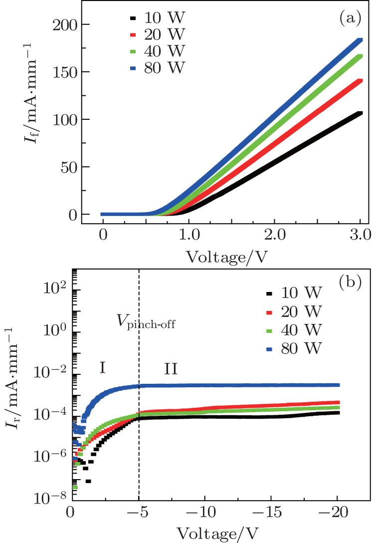
3. Result and discussionTypical current– voltage characteristics were measured to clarify the influence of dry-etching damage on the electrical properties for the recessed SBD. Figure 3 shows the typical experimental forward and reverse I– V characteristics of recessed SBD with Lac of 30 μ m, Von is defined as the voltage-axis intercept of the forward I– V curves in the linear region. To clarify the relationship between turn-on voltage and etching power, the plot of Von as a function of the recessed-anode etching power is shown in Fig. 4. It is clear that Von of the recessed SBD is lowered with the increase of RF power from 10 W to 80 W. A distinct reduction of Von as the etching power increases is observed. In the reverse bias, the leakage current shows two different behaviors above and below pinch-off voltage. In the reverse bias above pinch-off voltage, an increase of leakage current is observed when the etching power increases. However, when the reverse bias drops below the pinch-off voltage, leakage current saturates and Ir (reverse current) of samples with etching power from 10 W to 40 W remains in the same magnitude of 1× 10− 4 mA/mm. It indicates that leakage current below pinch-off voltage is independent of the etching power. Note that an exception of samples of 80-W etching power with leakage current of 1× 10− 2 mA/mm is observed as well. It is believed that the etching process with excessive etching power causes significant damage to the bulk material. The behaviors above suggest that increasing etching power in an appropriate range contributes to the reduction of the turn-on voltage without sacrificing the low leakage current of the recessed SBDs. This phenomenon has not been reported previously.
In order to give insight into the influence of dry-etching damage on the electrical properties above, current– voltage– temperature (I– V– T) measurements were performed over a range of 298 K < T < 473 K. In the forward bias, we took account of a tunneling transport component based on the thermionic-field emission (TFE) model to fit the experiment curves. A previous study has reported that TFE is the dominant current transport mechanism for the recessed AlGaN/GaN SBD. [9] Under the forward bias, the current due to TFE is given by[11, 12]

with


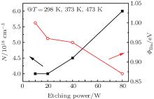
where A* is the Richardson constant, T is the absolute temperature, ϕ Bn is the Schottky barrier height (SBH), ϕ n = (EC − EF)/q, k is the Boltzmann constant, and E00 represents the tunneling characteristic energy. Here, ϕ Bn and N are taken as the fitting variables to fit in the experiment curves. Figure 5 shows the forward I– V– T curves of recessed AlGaN/GaN SBD and calculated I– V– T curves by the TFE model. The linear portion of the measured curves is fitted well to the calculated curves with N and ϕ Bn in a wide range of temperature from 298 K to 473 K. To illuminate the relationship of calculated concentration N and barrier height ϕ Bn to the RF power, a plot of N and ϕ Bn as a function of RF power is shown in Fig. 6. It is clear that the equivalent Schottky barrier height decreases with the increase of dry-etching power. The reduction of ϕ Bn is consistent with the reduction of Von. Moreover, doping concentration N of SBD was calculated as 4× 1018 cm− 3, 4× 1018 cm− 3, 4.5× 1018 cm− 3, and 6× 1018 cm− 3 for recessed-SBD with etching power of 10 W, 20 W, 40 W, and 80 W respectively. Note that the doping concentration N becomes larger as the ICP etching power increases. The calculated concentration is approximately the same magnitude as that of 2DEG. Therefore, the equivalent doping concentration N is related to the concentration of 2DEG channel. The increase of N suggests that the dry-etching process with high RF power induces additional donor-like defects, which contributes to the increase of concentration of the conductive channel. The higher the etching power in the process, the more defects will be induced to the channel. A recent theoretical study has proposed that the ICP etching process produces N vacancies (VN), [13, 14] which behave as donor states near the conduction band edge. As the dry-etching power increases, the ICP-etched surface including the sidewall becomes more N-deficient and produces VN-related defects. These defects and/or their complex may provide a conducting path with a lower barrier, which increases the tunneling probability for the thermally excited electrons. The lateral conducting path is conducted with lower Von. This explains the reason for the early conduction and reduction of Von.
To understand the influence of dry-etching damage on reverse leakage, current– voltage– temperature measurement was further performed in the reverse leakage bias. As discussed, reverse current transport through different paths when the reverse bias is above or below pinch-off voltage. Therefore, two different mechanisms are discussed separately.
(i) In the reverse bias above pinch-off voltage, the 2DEG channel under Schottky metal is not depleted completely. The reverse current path consists of the surface Ni/Au-AlGaN contact and the sidewall Ni/Au-GaN contact. The leakage current is codetermined by FP emission on the AlGaN surface and tunneling on the sidewall. To investigate the effects of the dry-etching power damage, the reverse experimental curves were fitted by Frenkel– Poole emission model. The current density calculated as the FP model is given by

where Eb is the electric field in the semiconductor barrier at the M– S interface and is assumed to be constant within the AlGaN barrier layer, ϕ t is the barrier height for electron emission from the trapped state, ε s is the relative dielectric permittivity at high frequency, T is the absolute temperature, and k is Boltzmann constant. In Eq. (4), the current transport equation can be rearranged as

where

As shown in Fig. 7(a) (only 20 W is given), the current ln(J/E) versus  plots of the measured reverse bias current density above pinch-off voltage (– 5 V < V < 0 V) are well described by the electric-field dependence of Eq. (5). Figure 7(b) shows the function of calculated ϕ t versus etching power of the ICP process based on the calculation of Eq. (6) from the slope of b(T) versus 1/T plots. The data points fit well with straight lines. Note that the calculated ϕ t is lowered as the etching power becomes higher. This trend may be due to the increasing recessed-sidewall tunneling currents. FP emission refers to electric-field-enhanced thermal emission from a trapped state into a continuum of electron states, [15] where ϕ t represents the emission barrier height for the trapped states. It can be concluded that the barrier height for the FP emission is lowered as the RF power becomes higher. When the RF power becomes higher, more traps are induced on the sidewall, which increase the tunneling probability for the lateral conduction path. Therefore, the total leakage current increases with the sidewall tunneling current.
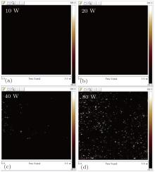
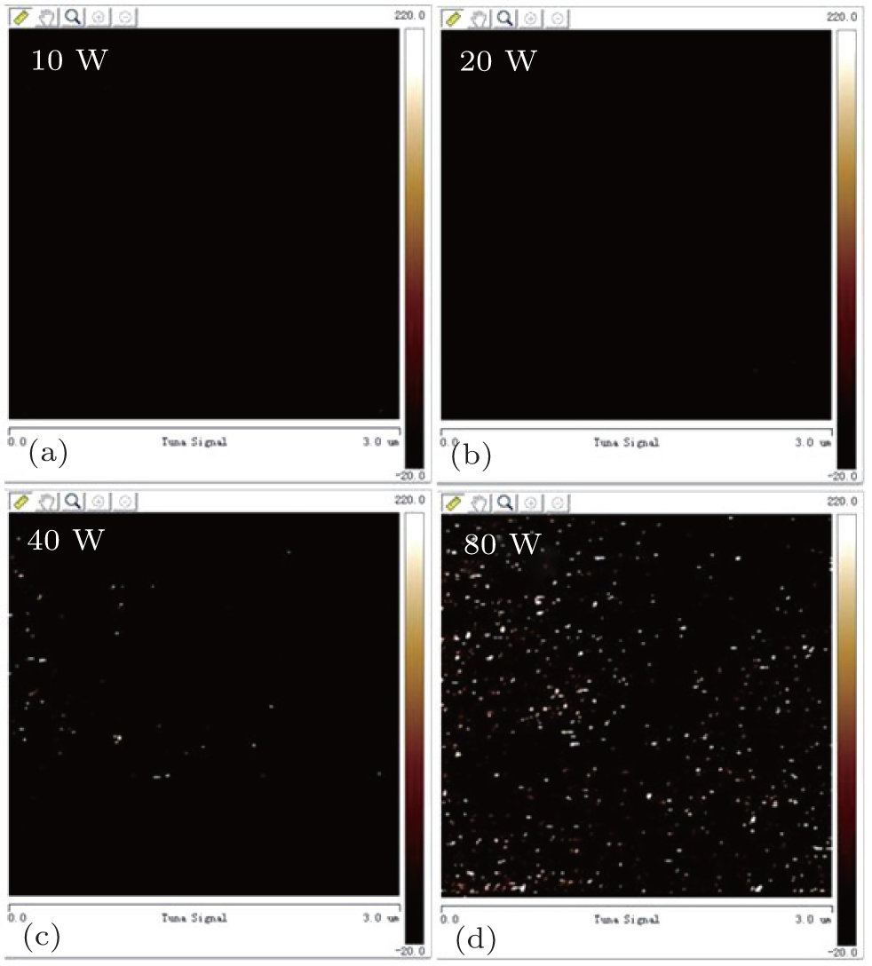
(ii) In the reverse bias below the pinch-off voltage (V < – 5 V), the 2DEG channel is completely blocked. The leakage current saturates and mainly transports through the vertical Schottky contact. The leakage current is only related to the trap concentration of the planar AlGaN surface, which is protected by photoresist during the etching process. As the surface is independent of the RF power, the leakage current should saturate in the same magnitude regardless of the change of RF power. However, in the condition of excessive RF power of 80 W, the device shows an undesired high leakage current. That is mainly due to the AlGaN surface damage induced by excessive RF power. Figure 8 shows conductive atomic-forced microscope (CAFM) scan pictures of AlGaN surfaces for SBDs. For the sample of 80 W, large quantities of leakage peaks appear on the AlGaN surface. As the mesa surface is protected by photoresist, it indicates that the etching process with excessive RF power would penetrate through the photoresist and cause significant damage to the AlGaN surface. Therefore, an appropriate RF power should be considered without any damage induced to the AlGaN surface.
According to the electrical properties and the I– V– T analysis above, the influence of the dry-etching damage can be explained as follows. Reductions of Von with the increase of RF power can be explained by TFE model. As the RF power increases, more defects are induced on the sidewall during the etching process, which increase the tunneling probability and result in early conduction. In the reverse bias above pinch-off voltage, the 2DEG channel under Schottky metal is not depleted completely and sidewall tunneling contributes to the total leakage current as calculated by the FP model. When the reverse bias is below the pinch-off voltage, the 2DEG channel is completely blocked and the leakage current is mainly transported through the vertical Schottky contact. However, when the excessive RF power is applied, the etching process would affect the AlGaN surface and cause the increase of the leakage current.


 ]
]