
Enhanced performances of AlGaInP-based light-emitting diodes with Schottky current blocking layers
[Ma Li† , Shen Guang-Di, Gao Zhi-Yuan, Xu Chen]
, Shen Guang-Di, Gao Zhi-Yuan, Xu Chen]
|
|


†Corresponding author. E-mail: mali@emails.bjut.edu.cn
*Project supported by the National Natural Science Foundation of China (Grant No. 11204009) and the Natural Science Foundation of Beijing, China (Grant No. 4142005).
A new epitaxial structure of AlGaInP-based light-emitting diode (LED) with a 0.5-μm GaP window layer was fabricated. In addition, indium tin oxide (ITO) and localized Cr deposition beneath the p-pad electrode were used as the current spreading layer and the Schottky current blocking layer (CBL), respectively. The results indicated that ITO and the Schottky CBL improve the total light extraction efficiency by relieving the current density crowding beneath the p-pad electrode. At the current of 20 mA, the light output power of the novel LED was 40% and 19% higher than those of the traditional LED and the new epitaxial LED without CBL. It was also found that the novel LED with ITO and CBL shows better thermal characteristics.
For applications as warm white light-emitting diodes (LEDs) and in general lighting, high-performance AlGaInP-based LEDs have attracted considerable interest.[1, 2] The internal quantum efficiency of the AlGaInP-based LEDs is nearly 100%, but the external efficiency is still limited by several problems, such as the large difference in the refractive index between the semiconductor and the air, current spreading, and substrate absorption.[3, 4] Among these problems, the poor current spreading effect seriously affects the external efficiency of LEDs. In the typical AlGaInP-based LEDs, the distance between the p-electrode and the active region is so short that the injected current has not spread to the chip edge yet when it reaches the active region, thus the inject current mainly exists right beneath the p-electrode.[5, 6] However, the light generated underneath the electrode cannot escape from the top chip due to the opaque metal. Even though some methods were proposed to solve this problem, such as inserting indium tin oxide (ITO)[7] and a high conductive window layer, [8] the current crowding under the p-pad electrode is still a major issue in the top-emission structure due to the poor current spreading.
To reduce the injected carriers beneath the p-electrode and expand the current distribution, several different current blocking layers (CBLs) have been adopted. Gaw et al. adopted a dielectric layer on the window layer beneath the p-electrode to prevent the injected current from flowing under the p-electrode.[9] However, this improvement is nearly useless when the window layer is thick enough because the carriers blocked at the surface will gradually spread inward under the p-pad electrode. Sugawara et al. inserted a p– n junction rectifier between the window layer and the cladding layer to function as a CBL.[10] The drawback of this technique is that the metal organic chemical vapor deposition (MOCVD) procedure needs to be performed twice, and it is very complex for LED fabrication. Wang et al. inserted a thick insulator layer in GaP under the p-pad.[11] This technique is effective for improving LED performances, but it is still too difficult to insert such a thick insulator layer with the current technology.
In this paper, we design a modified AlGaInP-based LED epitaxial structure with a thin GaP window layer and a Schottky CBL in GaP. The ITO layer is introduced as a current spreading layer, the CBL is made by metal Cr with a narrow bandgap so that it can form a Schottky contact with GaP. The results show that the performances of the LEDs with Schottky CBL and ITO layer are considerably enhanced compared to those of the conventional LEDs.
In this study, the epitaxial wafers were grown on GaAs substrates by MOCVD. The AlGaInP-based LED structure consists of a 0.22-μ m-thick Si-doped buffer layer, a GaAs/AlAs distributed Bragg reflector (DBR) layer, a 0.325-μ m-thick n-type cladding layer, an undoped 60-period (Al0.5Ga0.5)In0.5P/(Al0.1Ga0.9)In0.5P multiple quantum well (MQW) active region, and a 1.025-μ m-thick p-type cladding layer. As stated above, the CBL on the GaP layer seems in vain once the GaP layer is thick enough, similarly, a thin CBL in a thick GaP layer is also useless because the current will flow underneath the electrode by avoiding the CBL. For studying the effect of inserting a CBL in the GaP layer, we prepared the LED structure with a thin GaP layer, which was only 0.5 μ m thick. A 100-nm-thick ITO current spreading layer was subsequently deposited on the thin GaP by e-beam evaporation, then the ITO underneath the electrode was partially wet etched, the GaP exposed under the ITO layer was also etched by inductively coupled plasma (ICP) to the low concentration doping area. A 100-nm-thick Cr layer was sputtered on the area, thus a Schottky contact between GaP and Cr was formed as a CBL. Then BeAu (50 nm/300 nm) and AuGeNi/Au (50 nm/300 nm) were deposited as p-type and n-type contacts, respectively. Finally, the LEDs were annealed at 435 ° C for 30 s. A reference LED with the traditional LED structure and an 8-μ m-thick GaP layer was also prepared. To illustrate the effect of the CBL, LEDs with new epixial structure and ITO layer were also fabricated. The chip size of the LEDs in this study was 200 μ m× 200 μ m.
The current– voltage (I– V) characteristics were measured by Keithley 2430, and the light intensity and light output power of the LEDs were then measured by using the integrated sphere made in the Evefine Company.
Figures 1(a)– 1(c) show the schematic structures of the traditional LED, the new epitaxial LEDs without and with Schottky CBL, which are labeled as LED-I, LED-II, and LED-III, respectively.
 | Fig. 1. Schematic cross sections of (a) LED-I, (b) LED-II, and (c) LED-III. |
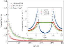
The lossy transmission line model proposed by Morgan et al.[12] assumes a constant potential and current density J0 under the metal. Then current density J(R) extending from the contact is given by J(R) = J0/(1 + R/Ls), where R is the distance away from the contact, Ls is the current spreading length given by 
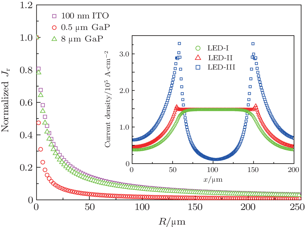 | Fig. 2. The injected current density Jr as a function of the radial distance from the contact edge for various current spreading layer thicknesses. The inset is the current density distributions across the active regions of the three devices. |
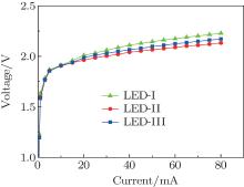
Figure 3 shows the typical current– voltage (I– V) characteristics of LED-I, LED-II, and LED-III. The characterization was performed for five randomly selected devices of each kind. As shown in Fig. 3, at 20 mA injection current, the measured forward voltages in LED-I, LED-II, and LED-III are 2.01 V, 1.968 V, and 1.989 V, respectively. This could be attributed to the difference in the conductivity between GaP and ITO. In the new LED structure, the current spreading layer consisting of a 0.5-μ m GaP and 100-nm ITO has higher conductivity and lower series resistance. On the other hand, compared to LED-II, LED-III has a slightly larger forward voltage due to the CBL design, which reduces the current flow area and the current conduction path.
 | Fig. 3. Forward characteristics of LED-I, LED-II, and LED-III. |
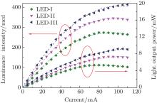
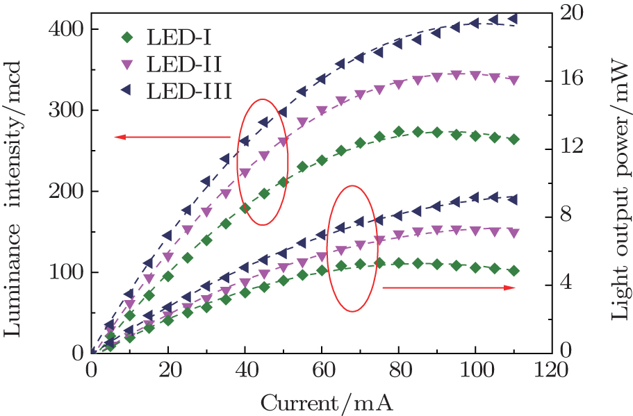
Figure 4 shows the luminance intensity and light output power versus the current for the three kinds of LEDs. LED-III presents higher performances, the luminance intensity (145 mcd) at 20 mA is about 1.5 times that of LED-I (95 mcd), and 1.2 times that of LED-II (120 mcd). The improvement could be attributed to the relatively high current density around the p-pad induced by the current blocking layer. LED-II has a luminance intensity exceeding that of LED-I by about 26%; this may be due to the better transmittance of ITO and the lower refractive index difference of ITO and air. At the injection current of 20 mA, the output powers of LED-I, LED-II, and LED-III are 1.94 mW, 2.27 mW, and 2.71 mW, respectively. The optical power of LED-III is enhanced by 40% compared to that of LED-I and by 19% compared to that of LED-II. The improvement in the optical power of LED-III is not so proud compared with the LED-I result. The reason is that the thick GaP layer of LED-I increases the lateral light power. In addition, LED-I and LED-II reach the power saturation at about 80 mA and 90 mA, respectively, which are lower than that of LED-III, meaning that the CBL could indeed decrease the heat generated in the active region. The properties comparison of LED-II and LED-III highlights the effect of the CBL; the CBL could improve the light extraction efficiency by about 20%.
 | Fig. 4. Luminance intensity and light output power versus the current in the three LEDs. |
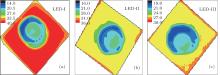
The thermal distributions in the three LEDs at 20 mA were measured by an infrared camera. For comparison, the test data were extracted to redraw the thermal images shown in Fig. 5. One can see that the temperature of LED-I is higher than that of the others. This can be attributed to the characteristic of GaP and the light emission under the p-pad. The thick GaP in LED-I increases the series resistance so the Joule heat increases. On the other hand, in LED-I, the current concentrates under the p-pad that the maximum light emission occurs especially beneath the p-pad. As stated above, light under the p-pad cannot escape from the chip because of the opaque metal, so it is absorbed by the material and then conversed to heat. On the contrary, LED-II and LED-III adopt an ITO layer and a thinner GaP window layer, which decrease the Joule heat in the devices. Compared with LED-II, LED-III has a lower temperature due to there being no light emission beneath the p-pad.
 | Fig. 5. Thermal distributions in LED-I, LED-II, and LED-III. |
A novel AlGaInP-based LED with a Schottky CBL embedded in the thin GaP window layer was proposed in order to provide a Schottky barrier beneath the p-pad. Because of the poor current transport capacity of the thin GaP layer, an ITO layer was also introduced. The experimental results showed that the light intensity and light output power can be obviously improved by using the Schottky CBL and ITO simultaneously. At a driving current of 20 mA, the light output power of the novel LED with Schottky CBL was increased by 40% compared to that of the traditional LEDs. The improvement is contributed to the Schottky CBL which can deflect the current away from the p-electrode pads. Better thermal characteristics of the novel LED were also demonstrated.
| 1 |
|
| 2 |
|
| 3 |
|
| 4 |
|
| 5 |
|
| 6 |
|
| 7 |
|
| 8 |
|
| 9 |
|
| 10 |
|
| 11 |
|
| 12 |
|