Effect of CuPc and MoO 3 co-evaporated layer on the conductivity of organic light emitting diodes
[He Ze-Shang, Yu Hao-Miao, Peng Huan, Hou Xiao-Yuan† ]
]
]
|
|


†Corresponding author. E-mail: xyhou@fudan.edu.cn
*Project supported by the Science and Technology Commission of Shanghai Municipality, China, the National Science and Technology Major Project of the Ministry of Science and Technology of China, and the National Natural Science Foundation of China.
Devices with copper phthalocyanine (CuPc):molybdenum trioxide (MoO3) co-evaporated layer were fabricated and the current–voltage ( I– V) and capacitance–voltage ( C– V) characteristics were measured. It has been found that for a given voltage, the current of the device with a co-evaporated layer is higher than those without the co-evaporated layer and it reaches the highest value if the ratio of MoO3 to CuPc is 1:1. Meanwhile, the C– V characteristics showed that only free holes exist in the function layer consisting of pure CuPc. However, charge transfer (CT) complexes exist in the function layer of a CuPc:MoO3 mixture. The charge transfer complexes do not contribute to the transport of the device efficiently under low applied fields but are disassociated into free carriers rapidly at applied fields higher than 1.7 × 10⁵ V/cm, which greatly increases the conductivity.
Conductivity is an important factor that can greatly impact the performance of devices, such as organic photovoltaic (OPV), organic light emitting diodes (OLED).[1– 5] However, the conductivity of organic small molecular materials is still poor compared with traditional inorganic materials because of their low charge mobility and low carrier density.[6, 7] In 2001, Zhou et al. found that the conductivity of TDATA can be greatly increased by F4-TCNQ doping.[8, 9] Then, in the last decade, transition metal oxides (TMO) as p-type dopants have been proposed to improve the conductivity of organic materials.[10– 15] Chang et al. showed that the WO3 is capable of accepting electrons from 2-TANTA to generate free holes, leading to conductivity improvement.[16] Meanwhile, Guan et al. measured the UV-vis absorption of doped film and found a red shift of CuPc’ s absorption peak. They attributed this red shift to the formation of a charge transfer complexes between CuPc and MoO3, resulting in the conductivity improvement.[17– 19] However, they have not shown the mechanism through which the conductivity is improved. Moreover, Qiao et al. found that the direction of charge transfer would be inversed if MoO3 is doped into different materials, so they concluded that charge transfer complexes would not result in the conductivity increase of the doped films.[20] Although many researchers have shown conductivity improvement, [16– 22] the mechanism is still a controversial subject. Some researchers believed that charge transfer complexes are really formed in the doping film and others have thought that the doping just increases the amount of the free holes rather than forming charge transfer complexes. In addition, whether the charge transfer complexes impact the mobility or if they participate in conduction directly is still not clear, although some researchers believed that they indeed exist in the devices.
In the present work, devices with CuPc:MoO3 coevaporated layer were fabricated and the current– voltage characteristics were measured. For a given voltage, the current of devices with the co-evaporated layer is higher than those without the co-evaporated layer and it reaches the highest value if the ratio of MoO3 to CuPc is 1:1. To explain this phenomenon, the capacitance– voltage characteristics were also measured and a U-shaped C– V curve has been obtained. The capacitance increases slowly under applied voltages lower than 2.4 V, corresponding to the electric field of 1.7 × 10⁵ V/cm, and it increases rapidly under the voltages higher than 2.4 V, for either bias polarity. The C– V characteristics showed that only free holes exist in the function layer consisting of pure CuPc but charge transfer complexes exist in the function layer of the CuPc:MoO3 mixture. The charge transfer complexes do not efficiently contribute to the conductivity of a device under low applied fields but would be disassociated rapidly into free carriers at applied fields higher than 1.7 × 10⁵ V/cm to greatly increase the conductivity.
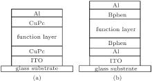
All of the devices were fabricated on pre-cleaned glass substrates coated with transparent conducting indium tin oxide (ITO) as the anode. The substrates were heated to 150 ° C in air after solvent cleaning, and they were then loaded into a high vacuum chamber (5 × 10− 5 Pa). Organic films were deposited after cooling down the substrates to room temperature. The deposition rates of the organic layer and Al cathode were 0.5 Å /s– 2 Å /s and 3 Å /s, respectively. The co-evaporated layer was deposited with both the CuPc and MoO3 sources. The prepared devices were all of area 9 mm2 with a 3-mm-wide ITO strip crossed over by a 3-mm-wide Al bar. Device A of structure ITO/CuPc(20 nm)/function layer(60 nm)/CuPc(20 nm)/Al was used for current– voltage characteristic measurement and device B of structure ITO/Al(5 nm)/Bphen(20 nm)/function layer(100 nm)/Bphen(20 nm)/Al (Bphen is a blocking layer to eliminate the influence of injection on capacitance) was used for capacitance– voltage characteristic measurement. Both structures are shown in Fig. 1. The function layer was a mixture of CuPc and MoO3, with different ratios of CuPc to MoO3.
 | Fig. 1. Structure of the prepared devices. (a) Device A. (b) Device B. |
The current– voltage (I– V) characteristics were measured by a Keithley 2440 and capacitance measurements were performed by a Keithley 4200 semiconductor characterization system with 4210-CVU and the ac signal was set as 1 kHz, 50 mV. The positive voltage (forward bias) was defined by a positively biased ITO electrode in all C– V measurements. All of the measurements were carried out in air at room temperature without illumination.
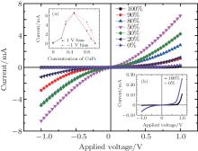
Figure 2 shows the current– voltage characteristics of device A with function layers of different CuPc concentrations (0%, 20%, 30%, 50%, 80%, 90%, and 100%). Inset (a) of Fig. 2 shows the current at 1 V bias and − 1 V bias, respectively, for different CuPc concentrations. The current is 0.258 mA (1 V) and 0.065 mA (− 1 V), respectively, for 0% CuPc concentration. The current increases with the CuPc concentration if it is lower than 50%. The device with 50% CuPc concentration shows the maximum current both at 1 V and − 1 V as 6.536 mA (1 V) and 6.726 mA (− 1 V), respectively. Then, the current decreases as CuPc concentration increases further. Finally, for the device with CuPc concentration 100%, the current is 0.108 mA (1 V) and 0.003 mA (− 1 V), respectively, which is much lower than that of the doped samples. Namely, the conductivity of CuPc layer would be improved by doping with MoO3 and most efficiently with a ratio of CuPc to MoO3 1:1.[18]
Inset (b) of Fig. 2 shows the I– V characteristics of a device with a function layer of pure CuPc or pure MoO3. The current– voltage characteristic of the device with a pure CuPc function layer shows typical features of rectification. In contrast, the device with a pure MoO3 function layer will be turned on for either bias polarity. Namely, MoO3 results in the turning on of the device both at positive and negative biases, while the device without MoO3 doping can only be turned on under a positive bias. Because the structure of each device A is the same except for different compositions of the function layer, the effects of electrode, CuPc layer, and the interface between them can be disregarded, while the contact of CuPc with MoO3 must play an important role in this phenomenon.
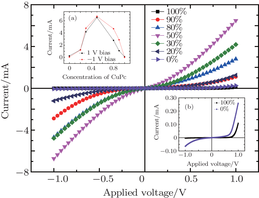 | Fig. 2. Current– voltage characteristics of device A with different CuPc concentrations. The function layer is formed of co-evaporated CuPc and MoO3. Inset (a) current under 1 V bias and − 1 V bias versus CuPc concentration. Inset (b) I– V of devices with a pure CuPc or MoO3 function layer. |
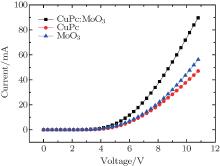
The current– voltage characteristics of OLED with different function layers were measured and are shown in Fig. 3. It can be seen that the current of the device with a co-evaporated layer could reach as high as 90 mA at 11 V bias, while the current of devices with pure MoO3 or CuPc is only 57 mA and 47 mA, respectively, at the same voltage. The current improvement by mixing CuPc with MoO3 is obvious. This result demonstrates that doping can indeed improve the conductivity of an OLED.
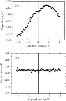
As mentioned in the introduction, whether free holes or charge transfer complexes would be responsible for the conductivity improvement has not yet been clarified.[16– 22] Besides, the real effect of charge transfer complexes is also not clear, although some researchers believe that they really exist in the devices. Here, a mechanism of conductivity improvement that charge transfer complexes existing in the co-evaporated layer would be dissociated by a high-applied electric field is proposed. In order to prove this idea, the capacitance– voltage characteristics of devices with different function layers were measured. Figure 4(a) shows the C– V curve of the device with a pure CuPc function layer. It is shown that the capacitance reaches a maximum 2.675 nF at a positive bias of 1.5 V. It has been reported that free holes exist in CuPc.[23] The capacitance decreasing away from its peak value could be attributed to the expansion of the space charge region (SCR) in the organic layer.[24] Therefore, the shape of C– V curve is evidence to show that only free holes exist in the device.
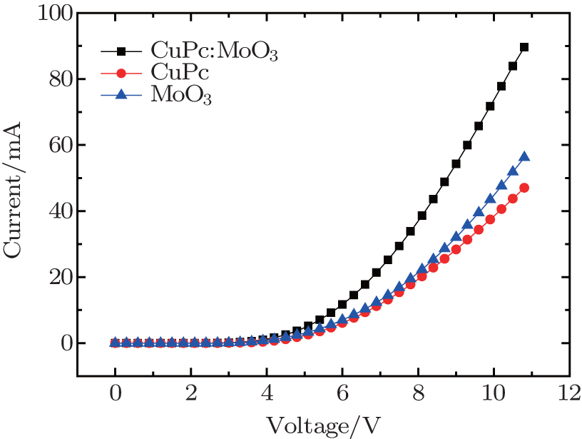 | Fig. 3. Current– voltage characteristics of devices with different function layers and structures of ITO/(function layer, 20 nm) /NPB(20 nm)/Alq3(40 nm)/LiF(1 nm)/Al. Solid squares, solid circles, and solid triangles correspond to the function layers of (CuPc:MoO3, 1:1), CuPc, and MoO3, respectively. |
Figure 4(b) shows the C– V curve of the device with a pure MoO3 function layer. It shows that no obvious relationship exists between capacitance and the applied voltage. The capacitance value fluctuates around 3.87 nF. Compared with the C– V relation of CuPc, it could be conclude that there are no free carriers existing in the pure MoO3 layer and the pure MoO3 layer would not affect the capacitance of the device.
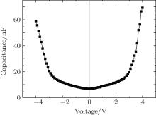
Figure 5 shows the C– V characteristic of the device with CuPc:MoO3 co-evaporated layer and a U-shaped relationship was obtained. Basically, the C– V relation for a positive bias can be divided into two regions. The first region is from 0 V to 2.4 V, where the capacitance increases almost linearly with a slope of about 2.9 nF/V. While under a higher voltage, the capacitance increases sharply with a much higher slope of 28.3 nF/V. The inflection point is at 2.4 V, corresponding to the electric field of 1.7 × 10⁵ V/cm. In addition, the C– V characteristic shows some polarity symmetry about the applied voltage. This means that the capacitance increasing with the voltage is independent of the direction of the electric field but depends on its magnitude.
With the existence of a blocking layer, no charges can be injected into the device. Therefore, the capacitance of the device changes only when there occurs a charge distribution in the co-evaporated layer.[25, 26] In contrast to the result of the pure CuPc function layer, the capacitance was not reduced by the upward bias. Evidently, this rising capacitance is far away from the attributions of pure CuPc. Meanwhile, as shown in Fig. 4(b), no changes in capacitance with the applied voltages from − 4 V to 4 V in the device with MoO3 layer were found, indicating that no charge generates in the MoO3 layer. In this sense, we attribute the capacitance increase to the mixture of CuPc and MoO3. Because the highest occupied molecular orbital (HOMO) of CuPc (− 5.2 eV) is higher than the lowest unoccupied molecular orbital (LUMO) MoO3 (− 6.3 eV), charges could transfer from CuPc to MoO3 and form charge transfer complexes, which has been reported in some previous studies.[25, 26]
 | Fig. 4. Capacitance– voltage characteristic of the device with structures (a) ITO/Al(5 nm)/Bphen(20 nm)/CuPc(100 nm)/Bphen(20 nm)/Al (the capacitance peak did not appear at 0 V bias is because the shift of zero point of built-in field) and (b) ITO/Al(5 nm)/Bphen(20 nm)/MoO3(100 nm)/Bphen(20 nm)/Al. |
The electric field induced dissociation of charge transfer complex will lead to a charge accumulation area adjacent to the blocking layers, and thus an increase of capacitance. The slow increase of capacitance under 0 V to 2.4 V bias indicates that the low electric field cannot dissociate charge transfer complexes efficiently, but the following sharp capacitance increase demonstrates that the charge transfer complexes would be dissociated rapidly under applied fields higher than 1.7 × 10⁵ V/cm.
Overall, the C– V characteristics indicate that charge transfer complexes are formed between CuPc and MoO3 and they can be dissociated by a relatively high applied field. When the charge transfer complexes are dissociated, the generated free charges will greatly improve the device’ s conductivity.
 | Fig. 5. C– V characteristic of the device with structure ITO/Al(5 nm)/ Bphen(20 nm)/(CuPc:MoO3, 1:1, 100 nm)/Bphen(20 nm)/Al. |
In summary, CuPc co-evaporated with MoO3 is an efficient way to improve the conductivity of an OLED. Charge transfer complexes which can be dissociated by a relatively high applied field are formed between CuPc and MoO3. When the charge transfer complexes are dissociated, the generated free holes and electrons will improve the device conductivity.
| 1 |
|
| 2 |
|
| 3 |
|
| 4 |
|
| 5 |
|
| 6 |
|
| 7 |
|
| 8 |
|
| 9 |
|
| 10 |
|
| 11 |
|
| 12 |
|
| 13 |
|
| 14 |
|
| 15 |
|
| 16 |
|
| 17 |
|
| 18 |
|
| 19 |
|
| 20 |
|
| 21 |
|
| 22 |
|
| 23 |
|
| 24 |
|
| 25 |
|
| 26 |
|