Zeng Fan, Zhang Wei-Bing†, Tang Bi-Yu‡. Electronic structures and elastic properties of monolayer and bilayer transition metal dichalcogenides MX2 ( M = Mo, W; X = O, S, Se, Te): A comparative first-principles study . Chinese Physics B, 24(9): 097103
Permissions
Electronic structures and elastic properties of monolayer and bilayer transition metal dichalcogenides MX2 ( M = Mo, W; X = O, S, Se, Te): A comparative first-principles study
*Project supported by the Construct Program of the Key Discipline in Hunan Province, China and Aid Program for Science and Technology Innovative Research Team in Higher Educational Institutions of Hunan Province, China.
Abstract
First-principle calculations with different exchange-correlation functionals, including LDA, PBE, and vdW-DF functional in the form of optB88-vdW, have been performed to investigate the electronic and elastic properties of two-dimensional transition metal dichalcogenides (TMDCs) with the formula of MX2( M = Mo, W; X = O, S, Se, Te) in both monolayer and bilayer structures. The calculated band structures show a direct band gap for monolayer TMDCs at the K point except for MoO2 and WO2. When the monolayers are stacked into a bilayer, the reduced indirect band gaps are found except for bilayer WTe2, in which the direct gap is still present at the K point. The calculated in-plane Young moduli are comparable to that of graphene, which promises possible application of TMDCs in future flexible and stretchable electronic devices. We also evaluated the performance of different functionals including LDA, PBE, and optB88-vdW in describing elastic moduli of TMDCs and found that LDA seems to be the most qualified method. Moreover, our calculations suggest that the Young moduli for bilayers are insensitive to stacking orders and the mechanical coupling between monolayers seems to be negligible.
PACS:
71.15.Nc; 62.20.de; 62.20.dj; 73.22.–f
Keyword:
transition metal dichalcogenides; bilayer structures; elastic properties; electronic structure
The successful isolation of graphene has brought in great revolutions for the modern material sciences.[1] The fascinating properties, such as the exceptionally high electron mobility (∼ 105 cm2· V− 1· s− 1)[2] and unique combination of high modulus (∼ 1000 GPa) and tensile strength (∼ 100 GPa), [3] have made graphene one of the most promising candidates for future flexible and stretchable electronics. However, the lack of band gap in pristine graphene limits its applications in reality. Due to the presence of a sizeable direct band gap in the visible frequency range, [4, 5] two-dimensional transition metal dichalcogenides (TMDCs) monolayers have been recently suggested as an important candidate for electronic and optoelectronic devices.[4― 6] Meanwhile, TMDCs also exhibit a number of intriguing optical phenomena such as valley-selective circular dichroism and the rich physics associated with the valley degree of freedom.[7] Moreover, their band gaps are tunable with thickness and different monolayer TMDCs can also be reassembled into designer van der Waals heterostructures, [8] which may lead to even richer physics and device applications.
Mechanical properties of materials such as elastic modulus are of vital importance in any practical device applications. It is thus a necessary prerequisite for the integration of TMDCs in various devices to obtain a detailed knowledge of mechanical properties of monolayer and two-dimensional (2D) heterostructures. Using nanoindentation in an atomic force microscope, Bertolazzi et al.[9] have investigated in-plane stiffness and breaking strength of suspended monolayer and bilayer MoS2, which indicated that monolayer MoS2 exhibits exceptional mechanical properties comparable to stainless steel. In-plane stiffness of monolayer and bilayer MoS2 were found to be 180± 60 N· m− 1 (corresponding to an effective Young’ s modulus of 270± 100 GPa) and 260± 70 N· m− 1 (200± 60 GPa), respectively. Recently, the elastic moduli of CVD grown monolayer MoS2 and WS2 and their bilayer heterostructures were also investigated.[10] High 2D elastic moduli of CVD monolayer MoS2 and WS2 (∼ 170 N· m− 1) were also found. The 2D moduli of their bilayer heterostructures were found to be lower than the sum of 2D modulus for each layer, which shows a strong mechanical interlayer coupling between the layers.[10]
The importance of mechanical properties in future device applications also intrigues theoretical interest. The in-plane stiffness of monolayer MoS2 has been investigated extensively.[11― 15] However, the scattered theoretical results from 124 to 146 N· m− 1 seems to be lower than the experimental value of 170 N· m− 1. Recently, the in-plane stiffness of a series of monolayer MX2 (M = Mo, W; X = S, Se, Te, O) has also been investigated by Kang et al.[13] and Ç akr et al.[14] Their results suggested that TMDCs with W (O) atom are found to be much stiffer in each chalcogenide (metal) group. It should be noticed that the Young modulus of TMDCs obtained using PBE functional seems to be lower than the experimental measure as shown above, it is thus interesting to evaluate the performance of commonly-used functionals to describe the mechanical properties of TMDCs. On the other hand, in contrast to the extensive studies for monolayers, elastic and mechanical properties of bilayer TMDCs are still lacking completely. Previous study has suggested a transition from direct gap in the monolayer to indirect gap in the bilayer for TMDCs, [4, 16― 18] which implies a strong electronic coupling between different monolayers in bilayer TMDCs. Meanwhile, stacking order is also found to affect the electronic band structure and absorption spectra.[19] It is thus quite interesting to investigate mechanical coupling between monolayers and to reveal the role of stacking order on the elastic property of bilayer TMDs theoretically.
To understand the electronic and mechanical coupling of monolayers in bilayer TMDCs, we have investigated electronic and elastic properties of eight kinds of TMDCs in both monolayer and bilayer structures, in which different functionals are employed for comparison. The detailed structures, electronic properties, elastic constants, and Young moduli of TMDCs both in monolayer and bilayer obtained using LDA, PBE, and optB88-vdW functional are given and compared with the available experimental and theoretical results. Moreover, the performance of different functionals in describing the elastic properties of TMDCs is also evaluated.
2. Computational details
The present calculations were performed with the Vienna ab-initio simulation package (VASP) code[20, 21] within the projector augmented wave (PAW) method. The local density approximation (LDA) and Perdew– Burke– Ernzerhof (PBE) were used in our calculation for comparison. To take into account van der Waals forces, which are expected to play a crucial role in the bilayer, the van der Waals density functional in the form of optB88-vdW[22, 23] was used. Recent study has evidenced that the optB88-vdW can give much improved results for the graphene/metal surface.[24] Cut off energy and Brillouin zone (BZ) sampling were determined after an extensive convergence test. The Brillouin zone was simplified by an (18× 18× 1) Monkhorst– Pack grid and a plane-wave basis set with kinetic cutoff energy of 550 eV was applied. The atomic positions of those 2D TMDCs have been optimized by using the conjugate-gradient (CG) algorithm. A vacuum of 20 Å was set to prevent interactions between periodic images. The elastic constants were obtained by strain– energy method. By applying a set of suitable deformations to the single unit cell of the 2D TMDCs, we obtained the energy– strain curves and the corresponding elastic constant. The detailed relationships between the applied strain and the elastic constant have been shown in Ref. [25]. The strains ranging from − 0.05 to 0.05 in steps of 0.01 were used in the present calculation.
3. Results and discussion
3.1. Monolayer TMDCs
3.1.1. Structure properties
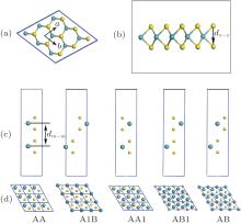
The structure of monolayer TMDCs is shown in Fig. 1(a), in which the M and X atoms occupy the hexagonal honeycomb site alternately. Due to the chemical ratio of M : X = 1:2, the M sublattice layer is sandwiched between two nearby X sublattice layers and forms an X– M– X covalently bonded hexagonal quasi-2D lattice as shown in Fig. 1(b), rather than the planar construction of the graphene.
Fig. 1. Top view (a) and side view (b) of the monolayer TMDCs. Panels (c) and (d) are stacking structures for bilayer. Yellow balls and green balls represent metal and chalcogen atoms respectively. Here, dx− x and dm− m mean the bond lengths of two X atoms and two M atoms, respectively.
The optimized structural parameters of TMDCs with LDA, PBE, and optB88-vdW methods are listed in Table 1, two previous PBE calculations[13, 14] are listed for comparison. We can find that the previous calculations are almost identical to our PBE results, which suggests that the present results are reliable. It can be clearly seen that the structure seems to be independent of the metal element but increases monotonously with the atomic number of chalcogen. In addition, it can also be found that LDA calculation gives a smaller value than PBE, while the results of PBE and optB88-vdW are almost the same, which are also closer to bulk crystals. This is in agreement with the well accepted knowledge that LDA overestimates the binding of materials. The similar results of PBE and optB88-vdW indicate that van der Waals functional can provide a balanced description for systems dominated by not only vdW force but also covalence bonding, and van der Waals interaction has few effects on such a monolayer TMDCs.
Table 1.
Table 1.
Table 1. The optimized structural parameters of monolayer TMDCs using LDA, PBE, and optB88-vdW methods. Here, a and dx− x represent the lattice constant and the bond length of two X atoms, respectively. The PBE results from Refs. [13] and [14] are also listed for comparison.
Table 1. The optimized structural parameters of monolayer TMDCs using LDA, PBE, and optB88-vdW methods. Here, a and dx− x represent the lattice constant and the bond length of two X atoms, respectively. The PBE results from Refs. [13] and [14] are also listed for comparison.
3.1.2. Electronic properties
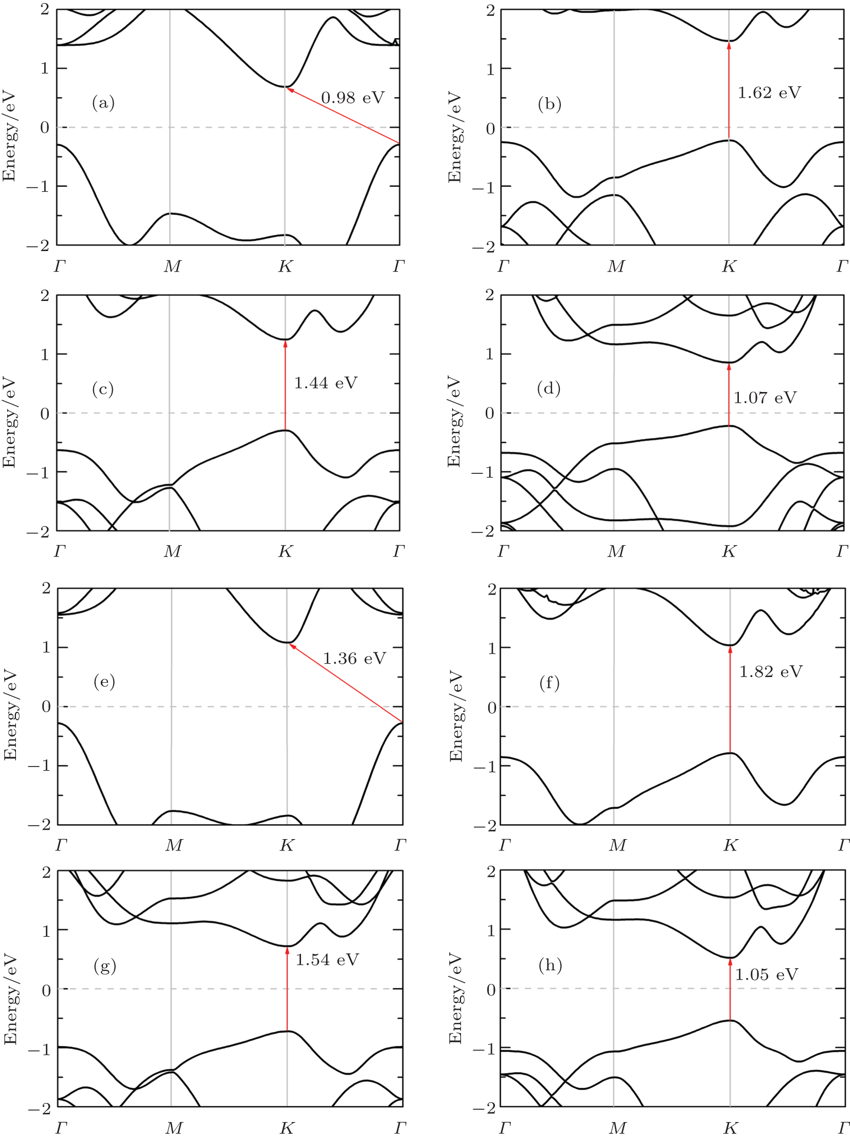
Now, we focus on band structures of monolayer TMDCs. Since the (semi)-local functionals are known to give a similar band structure for materials, we only give the energy band of monolayer TMDCs calculated using PBE functional. As shown in Fig. 2, all those eight kinds of single layer TMDCs are semiconductors with a distinct band gap, which is quite different from the zero-band-gap graphene. For example, the monolayer MoS2 has a direct band gap at the K point with a band gap value of 1.62 eV, which is close to the experimental study for atomically thin MoS2 layers.[4, 5] The direct band gap at the K point can also be found in the cases of monolayer MoSe2 and MoTe2, and the corresponding band gaps are 1.44 eV and 1.07 eV, respectively. However, for the case of MoO2, the band gap is indirect with a value of 0.98 eV. For monolayer MX2 (where M represents Mo and W) with direct energy gaps, the band gaps decrease when the chalcogenides element becomes heavier i.e., the energy gap order is disulfide> diselenide > ditelluride. To analyze the underlying mechanism, we have performed Bader charge analysis, which is known to be able to get the charge transfer between different atomic species. Taking MoX2 as an example, we can find the total charges of Mo atom in monolayer MoX2 are 4.29e, 4.52e, and 5.06e, which suggests that the charges transferred from metal to chalcogen atom are 1.71e, 1.48e, and 0.94e, respectively. This indicates that the reactivity and binding decrease from S to Te, which can also be supported by the fact that the lattice constants decrease with the row number of X in Mo dichalcogenides. Clearly, the strong reactivity of the chalcogen atom will enhance the hybridization, which will lead to a larger band gap of the compounds. In addition, the band gap for MoX2 (X = Se, S) seems to be smaller than WX2, and MoTe2 and WTe2 have quite close gaps. However, for monolayer oxide with indirect-band-gap, the band gap of WO2 is much larger than that of MoO2. The calculated band gaps agree well with other studies.[13, 27]
3.1.3. Elastic properties
Elastic property is another important physics quantity studied in the present work. For 2D TMDCs, it is possible to measure the elastic constants of these materials from nanoindentation experiments using an atomic force microscope.[28] However, since the experimental measurement suffers from some uncertainness such as defect, the first-principle calculation can offer an important supplement to the experiment.
The elastic constants for monolayer TMDCs calculated with PBE method are reported in Table 2. Since the monolayers of 2H-MX2 belong to isotropic structures, the linear elastic constant C22 is equal to C11. Linear elastic constants of MoX2 and WX2 decrease monotonically with the increase of chalcogen’ s atomic number, which means the decrease of the Young modulus, and for the same chalcogenide atoms, the WX2 compounds have a larger elastic constant than MoX2 compounds. The Poisson ratio used to describe the lateral deformation is calculated by ν = C12/C11. It is remarkable that the Poisson ratios of those 2D TMDCs are larger than that of graphene except for WTe2, which means much better lateral contraction property than graphene. The calculated Poisson ratio for MoS2 is also close to the results of other studies.[12, 14]
For further discussion of elastic properties of those monolayer TMDCs, we also evaluate the Young modulus . As shown in Table 3, the Young moduli from different methods are close to each other. The values for PBE and optB88-vdW are almost the same, while the results of LDA are larger than others. Although there are some numerical differences, the results of three methods present the same trends that Young moduli decrease with the atomic number of chalcogen and increase from Mo to W compounds. As shown above, charge transfer decreases and lattice constant increases in transition metal dichalcogenides MX2 when X changes from S to Te, which suggests that the reactivity and binding decrease from MS2 to MTe2. The weakening binding between the metal and the chalcogen atom thus leads to the smaller Young modulus. In addition, we can also find that the Young moduli for those monolayer TMDCs are comparable to that for graphene. For instance, Young moduli for MoO2 and WO2 are almost two-thirds of that for the graphene, which is relatively high. MoS2, MoSe2, WS2, and WSe2 have values about one-third of that for the graphene showing an excellent elastic property. The calculated Young moduli (141 N· m− 1 and 156 N· m− 1) using LDA for monolayer MoS2 and WS2 agree well with theoretical results[13, 14] and experiment measurement results (180± 60 N· m− 1[9] or around 170 N· m− 1[10]). We can also find that LDA calculations gave the closest results to experimental results among three functionals, which suggest that LDA calculations are more accurate to describe the elastic property of monolayer TMDCs.
Fig. 2. The band structures for monolayer TMDCs calculated using PBE. Panels (a)– (h) represent MoO2, MoS2, MoSe2, MoTe2, WO2, WS2, WSe2, and WTe2, respectively. The Fermi energy is marked with light gray dashed lines. The band gaps are shown with red arrows.
Table 2.
Table 2.
Table 2. The calculated elastic constants of monolayer TMDCs in units of N· m− 1 calculated using PBE functional. The data of graphene is also listed for comparison.
MoO2
MoS2
MoSe2
MoTe2
WO2
WS2
WSe2
WTe2
graphene
C11
232.92
134.89
110.7
84.72
253.25
148.47
122.01
91.42
351.6
C12
84.67
32.03
25.66
20.25
91.32
31.20
22.91
15.40
64.10
C44
74.12
51.43
42.52
32.23
80.96
58.63
43.03
38.01
143.75
ν
0.36
0.24
0.23
0.24
0.36
0.21
0.19
0.17
0.18
Table 2. The calculated elastic constants of monolayer TMDCs in units of N· m− 1 calculated using PBE functional. The data of graphene is also listed for comparison.
Table 3.
Table 3.
Table 3. The Young moduli of TMDCs in units of N· m− 1 with PBE, LDA, and vdW-DF(optB88-vdW) methods.
PBE
LDA
optB88
MoO2
202.1
221.8
199.8
MoS2
127.3
141.2
123.5
MoSe2
104.8
120.9
105.7
MoTe2
79.9
94.07
80.7
WO2
220.3
254.3
219.7
WS2
141.9
156.4
140.7
WSe2
114.4
132.8
118.2
WTe2
88.8
101.8
88.4
Table 3. The Young moduli of TMDCs in units of N· m− 1 with PBE, LDA, and vdW-DF(optB88-vdW) methods.
3.2. Bilayer TMDCs
3.2.1. Structure properties
There are different configurations when monolayers are stacked into bilayer structure.[19] As Fig. 1(c) shows, five stacking orders for the bilayer TMDCs are considered in this paper. Since the optB88-vdW can give a very similar in-plane lattice parameter with PBE and the interlayer interaction is dominated by vdW forces, we only analyze the results of the bilayer TMDCs using optB88-vdW functional. LDA calculation is also performed for comparison. The AA1 and AB with almost degenerate energy are found to be the most stable configuration for all bilayer TMDCs, which also agrees with the earlier calculations.[19] Firstly, we also give the structure parameters with five different stacking orders using LDA and optB88-vdW methods in Table 4. We can find that, the stack of the monolayer does not change the monolayer structure much. The lattice constants of monolayer and bilayer TMDCs are almost the same as these obtained by both LDA and optB88-vdW methods, while the inter-layer distances represented as dm− m varies with the stacking order. Both methods predict that the AA and AB1 stacking order have a larger value of dm− m than other stacking orders, while the distance for AA1 is the smallest, which agrees with the stability order of those configurations. The interlayer distances for bilayer TMDCs range from 5.2 to 7.8 Å according to our calculation. It is clearly shown that the structural parameters including in-plane lattice parameter and inter-layer distance obtained from LDA are much smaller than that of optB88-vdW for the same bilayer structures.
Table 4.
Table 4.
Table 4. The optimized structural parameters of bilayer TMDCs using LDA and optB88-vdW methods. Here, a represents lattice constant, dm− m is the distance of the metal atoms between different layers.
Stacking order
A1B
AA
AA1
AB
AB1
a/Å
dm− m/Å
a/Å
dm− m/Å
a/Å
dm− m/Å
a/Å
dm− m/Å
a/Å
dm− m/Å
MoO2
LDA
2.79
4.81
2.79
5.30
2.79
4.86
2.79
4.82
2.79
5.28
optB88
2.83
5.28
2.83
5.69
2.83
5.23
2.83
5.20
2.83
5.54
MoS2
LDA
3.12
6.09
3.12
6.80
3.12
6.01
3.12
5.98
3.12
6.68
optB88
3.18
6.36
3.19
6.75
3.19
6.28
3.19
6.24
3.19
6.71
MoSe2
LDA
3.25
6.52
3.25
7.05
3.25
6.33
3.25
6.35
3.25
7.05
optB88
3.33
6.64
3.32
7.14
3.32
6.57
3.33
6.57
3.32
7.09
MoTe2
LDA
3.47
7.08
3.46
7.73
3.47
6.85
3.47
6.89
3.47
7.71
optB88
3.56
7.25
3.56
7.78
3.56
7.10
3.56
7.11
3.56
7.75
WO2
LDA
2.79
4.88
2.79
5.34
2.79
4.90
2.79
4.87
2.79
5.31
optB88
2.83
5.27
2.83
5.68
2.83
5.22
2.83
5.19
2.83
5.58
WS2
LDA
3.13
6.18
3.13
6.81
3.13
6.06
3.13
6.04
3.12
6.69
optB88
3.18
6.37
3.19
6.82
3.19
6.29
3.19
6.26
3.19
6.73
WSe2
LDA
3.25
6.54
3.25
7.14
3.25
6.39
3.25
6.44
3.25
7.1
optB88
3.33
6.70
3.33
7.15
3.33
6.54
3.33
6.61
3.33
7.14
WTe2
LDA
3.47
7.13
3.47
7.76
3.47
6.87
3.47
6.95
3.47
7.72
optB88
3.57
7.27
3.56
7.79
3.56
7.12
3.57
7.12
3.56
7.76
Table 4. The optimized structural parameters of bilayer TMDCs using LDA and optB88-vdW methods. Here, a represents lattice constant, dm− m is the distance of the metal atoms between different layers.
3.2.2. Electronic properties
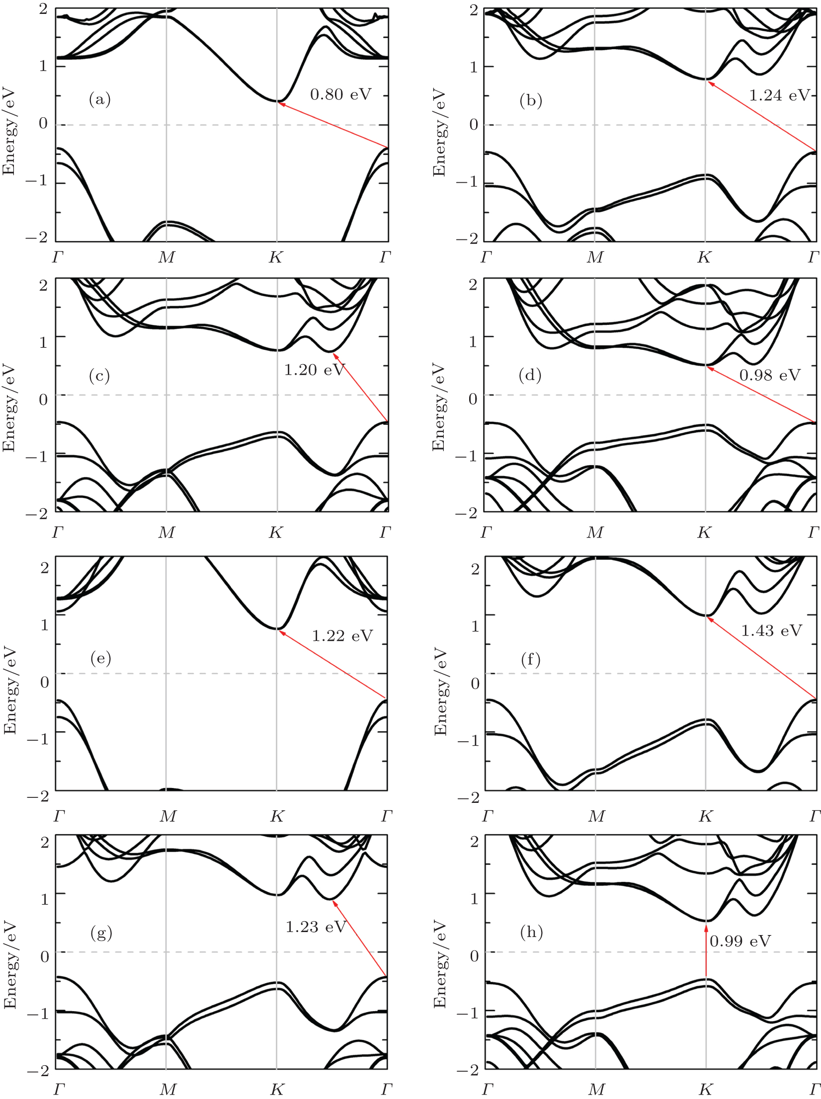
The band gaps of TMDCs are known to be tunable with thickness.[5, 10, 29] It is thus interesting to investigate the electronic structure of bilayer TMDCs. Since the low-energy AA1 and AB are found to have similar band structures, we only give the band structures of bilayer TMDCs in AA1 stacking order in Fig. 3. Unlike the direct band gap of monolayers, indirect band gap is found except for bilayer WTe2 which still has a direct band gap at the K points as shown in Fig. 3(h). We can easily find that the band gaps have the same variation behavior as the monolayers from MO2 to MTe2. It has to be mentioned that the valence-band maximum (VBM) of bilayer WTe2 at K point is only 0.06 eV larger than the maximum energy for Γ point, which is much smaller than energy difference in other cases. When monolayers are stacked into bilayers, the band gaps were found to decrease, which agrees well with previous theoretical studies.[19, 30]
Fig. 3. The band structures for monolayer TMDCs calculated using PBE. Panel (a)– (h) represents MoO2, MoS2, MoSe2, MoTe2, WO2, WS2, WSe2, and WTe2, respectively. The Fermi energy is marked with light gray dashed lines. The band gaps are shown with red arrows.
3.2.3. Elastic properties
To reveal the evolution of mechanical properties of TMDCs with thickness, we also calculated the elastic constants, Young modulus, and Poisson ratio of bilayer TMDCs in Table 5. The trend of bilayer Young modulus is very similar to that of monolayers. A decrease of Young modulus is found from MO2 to MTe2 and the Young modulus of WX2 is larger than that of MoX2. The Young moduli of AA and AB1 stacking orders are found to be larger than the others according to LDA. Meanwhile, we also find the differences of Young moduli for different stacking orders are within 5%, which indicates that the stacking order has little influence on the elastic properties of the bilayer. Compared with optB88-vdW functional, LDA has a larger Young modulus. In particular, LDA method predicts the Young moduli of around 280 N· m− 1 for bilayer MoS2, which is consistent with the recent experiment 300± 13 N· m− 1.[10] Table 5 also shows the Poisson ratios of bilayers of TMDCs with different configurations. The calculated results show that these bilayers have close Poisson ratios to the corresponding monolayer. Among different TMDCs bilayer, MoS2, MoSe2, and MoTe2 have similar Poisson ratios with the value of 0.2, which is also independent of the stacking order, while the Poisson ratios for bilayer WSe2 and WTe2, are found to be much smaller than that of the others. We also notice that optB88-vdW predicts larger Poisson ratios than LDA.
Table 5.
Table 5.
Table 5. Young moduli and Poisson ratios for bilayer TMDCs with different stacking orders.
Young modulus/N· m− 1
A1B
AA
AA1
AB
AB1
LDA
optB88
LDA
optB88
LDA
optB88
LDA
optB88
LDA
optB88
MoO2
439.7
400.7
442.3
399.9
439.4
398.9
438.9
399.8
441.2
405.5
MoS2
281.9
255.7
285.9
249.9
282.0
252.2
276.4
254.0
283.2
248.2
MoSe2
236.9
210.4
241.1
213.4
238.2
212.8
236.1
212.2
240.7
213.7
MoTe2
182.9
163.0
189.0
167.7
186.6
162.0
182.1
158.6
186.8
161.7
WO2
503.4
461.9
509.1
470.8
504.2
471.1
503.9
468.9
509.6
461.9
WS2
314.1
291.7
313.2
279.6
309.7
282.2
309.9
280.7
313.7
282.3
WSe2
262.2
232.4
265.7
233.2
265.1
227.3
262.5
234.3
266.1
232.5
WTe2
198.8
172.5
204.1
177.9
203.2
175.9
200.1
172.3
202.9
176.9
Poisson ratio
A1B
AA
AA1
AB
AB1
LDA
optB88
LDA
optB88
LDA
optB88
LDA
optB88
LDA
optB88
MoO2
0.365
0.364
0.366
0.367
0.365
0.367
0.369
0.37
0.365
0.353
MoS2
0.212
0.239
0.199
0.253
0.227
0.247
0.218
0.234
0.222
0.256
MoSe2
0.201
0.224
0.205
0.232
0.214
0.230
0.211
0.223
0.209
0.229
MoTe2
0.202
0.221
0.210
0.218
0.213
0.242
0.217
0.248
0.212
0.245
WO2
0.342
0.348
0.337
0.331
0.336
0.329
0.341
0.332
0.340
0.348
WS2
0.180
0.194
0.195
0.220
0.201
0.219
0.198
0.213
0.197
0.216
WSe2
0.173
0.191
0.179
0.200
0.174
0.217
0.174
0.189
0.175
0.204
WTe2
0.154
0.193
0.155
0.188
0.159
0.199
0.160
0.201
0.158
0.189
Table 5. Young moduli and Poisson ratios for bilayer TMDCs with different stacking orders.
It should be noticed that the inter-layer interaction is known to be predominated by vdW interaction, an accurate description for such a system may need a more advanced treatment such as RPA. However, on the basis of the reasonable description for elastic properties of TMDCs, LDA method may be an alternative to describe the elastic properties of bilayer TMDCs. Recently, Liu et al.[10] have investigated the elastic modulus of CVD grown monolayer MoS2 and WS2 and their bilayer heterostructures and found that the 2D moduli of their bilayer heterostructures are lower than the sum of 2D modulus of each layer, which shows a strong mechanical inter-layer coupling between the layers. However, according to the present results, the Young modulus of bilayer structure calculated by both LDA and optB88-vdW is almost twice that of the corresponding monolayer, which shows that the mechanical coupling between monolayers seems to be negligible in bilayers. Considered the experimental uncertainty, further effort both in experimental and theory is thus suggested to investigate the mechanical coupling of monolayers in bilayer.
4. Conclusion
We have investigated the band structure and elastic properties for eight kinds of two-dimensional TMDCs in monolayer and different bilayers using different functionals. Our results indicate that all those monolayers and bilayers belong to semiconductors and there is a transition from direct gaps for monolayers (except for MoO2 and WO2), into indirect gaps in bilayers (except WTe2). The calculation also shows that the monolayer TMDCs present excellent elastic properties, which are comparable to graphene. Meanwhile, we also find that the LDA method is an efficient alternative to more advanced methods in describing the elastic properties of both monolayer and bilayer TMDCs. Furthermore, our results also show that the elastic property is only influenced slightly by stacking order and the mechanical coupling between monolayers seems to be negligible.
... [1] The fascinating properties, such as the exceptionally high electron mobility (#cod#x223C ...
1
2008
0.0
0.0
... 1)[2] and unique combination of high modulus (#cod#x223C ...
1
2008
0.0
0.0
... GPa),[3] have made graphene one of the most promising candidates for future flexible and stretchable electronics ...
4
2010
0.0
0.0
... Due to the presence of a sizeable direct band gap in the visible frequency range,[4,5] two-dimensional transition metal dichalcogenides (TMDCs) monolayers have been recently suggested as an important candidate for electronic and optoelectronic devices ...
... [4#cod#x2015 ...
... Previous study has suggested a transition from direct gap in the monolayer to indirect gap in the bilayer for TMDCs,[4,16#cod#x2015 ...
... [4,5] The direct band gap at the K point can also be found in the cases of monolayer MoSe2 and MoTe2, and the corresponding band gaps are 1 ...
3
2010
0.0
0.0
... Due to the presence of a sizeable direct band gap in the visible frequency range,[4,5] two-dimensional transition metal dichalcogenides (TMDCs) monolayers have been recently suggested as an important candidate for electronic and optoelectronic devices ...
... [4,5] The direct band gap at the K point can also be found in the cases of monolayer MoSe2 and MoTe2, and the corresponding band gaps are 1 ...
... [5,10,29] It is thus interesting to investigate the electronic structure of bilayer TMDCs ...
1
2012
0.0
0.0
... 6] Meanwhile, TMDCs also exhibit a number of intriguing optical phenomena such as valley-selective circular dichroism and the rich physics associated with the valley degree of freedom ...
1
2014
0.0
0.0
... [7] Moreover, their band gaps are tunable with thickness and different monolayer TMDCs can also be reassembled into designer van der Waals heterostructures,[8] which may lead to even richer physics and device applications ...
1
2013
0.0
0.0
... [7] Moreover, their band gaps are tunable with thickness and different monolayer TMDCs can also be reassembled into designer van der Waals heterostructures,[8] which may lead to even richer physics and device applications ...
2
2011
0.0
0.0
... [9] have investigated in-plane stiffness and breaking strength of suspended monolayer and bilayer MoS2, which indicated that monolayer MoS2 exhibits exceptional mechanical properties comparable to stainless steel ...
... 1[9] or around 170#cod#x00A0 ...
6
2014
0.0
0.0
... [10] High 2D elastic moduli of CVD monolayer MoS2 and WS2 (#cod#x223C ...
... [10] ...
... 1[10]) ...
... [5,10,29] It is thus interesting to investigate the electronic structure of bilayer TMDCs ...
... [10] Table#cod#x00A0 ...
... [10] have investigated the elastic modulus of CVD grown monolayer MoS2 and WS2 and their bilayer heterostructures and found that the 2D moduli of their bilayer heterostructures are lower than the sum of 2D modulus of each layer, which shows a strong mechanical inter-layer coupling between the layers ...
1
2011
0.0
0.0
... [11#cod#x2015 ...
1
2013
0.0
0.0
... [12,14] ...
4
2013
0.0
0.0
... [13] and #cod#x00C7 ...
... 1, two previous PBE calculations[13,14] are listed for comparison ...
... [13,27] ...
... 1) using LDA for monolayer MoS2 and WS2 agree well with theoretical results[13,14] and experiment measurement results (180#cod#x00B1 ...
4
2014
0.0
0.0
... [14] Their results suggested that TMDCs with W (O) atom are found to be much stiffer in each chalcogenide (metal) group ...
... 1, two previous PBE calculations[13,14] are listed for comparison ...
... [12,14] ...
... 1) using LDA for monolayer MoS2 and WS2 agree well with theoretical results[13,14] and experiment measurement results (180#cod#x00B1 ...
1
2015
0.0
0.0
... 15] However, the scattered theoretical results from 124 to 146#cod#x00A0 ...
1
2013
0.0
0.0
... Previous study has suggested a transition from direct gap in the monolayer to indirect gap in the bilayer for TMDCs,[4,16#cod#x2015 ...
1
2012
0.0
0.0
1
2011
0.0
0.0
... 18] which implies a strong electronic coupling between different monolayers in bilayer TMDCs ...
4
2014
0.0
0.0
... [19] It is thus quite interesting to investigate mechanical coupling between monolayers and to reveal the role of stacking order on the elastic property of bilayer TMDs theoretically ...
... [19] As Fig ...
... [19] Firstly, we also give the structure parameters with five different stacking orders using LDA and optB88-vdW methods in Table#cod#x00A0 ...
... [19,30] ...
1
1993
0.0
0.0
... Computational detailsThe present calculations were performed with the Vienna ab-initio simulation package (VASP) code[20,21] within the projector augmented wave (PAW) method ...
1
1996
0.0
0.0
... Computational detailsThe present calculations were performed with the Vienna ab-initio simulation package (VASP) code[20,21] within the projector augmented wave (PAW) method ...
1
2010
0.0
0.0
... To take into account van der Waals forces, which are expected to play a crucial role in the bilayer, the van der Waals density functional in the form of optB88-vdW[22,23] was used ...
1
2011
0.0
0.0
... To take into account van der Waals forces, which are expected to play a crucial role in the bilayer, the van der Waals density functional in the form of optB88-vdW[22,23] was used ...
1
2014
0.0
0.0
... [24] Cut off energy and Brillouin zone (BZ) sampling were determined after an extensive convergence test ...
1
2010
0.0
0.0
... [25] ...
1
2011
0.0
0.0
1
2013
0.0
0.0
... [13,27] ...
1
2012
0.0
0.0
... [28] However, since the experimental measurement suffers from some uncertainness such as defect, the first-principle calculation can offer an important supplement to the experiment ...
1
2013
0.0
0.0
... [5,10,29] It is thus interesting to investigate the electronic structure of bilayer TMDCs ...
1
2012
0.0
0.0
... [19,30] ...
Electronic structures and elastic properties of monolayer and bilayer transition metal dichalcogenides MX2 ( M = Mo, W; X = O, S, Se, Te): A comparative first-principles study


 , Tang Bi-Yu‡