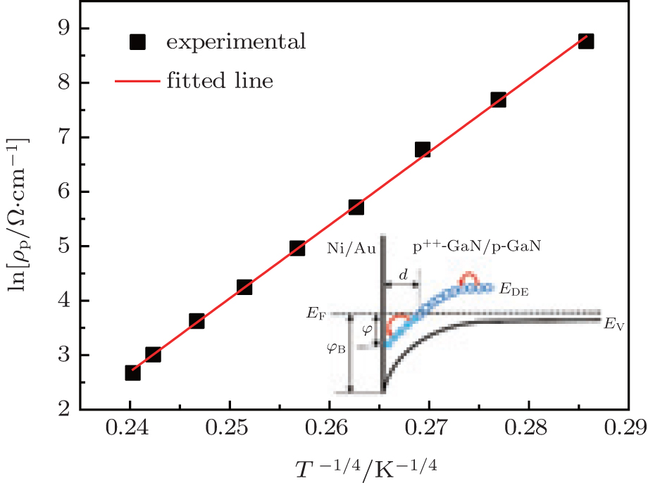
Influence of a deep-level-defect band formed in a heavily Mg-doped GaN contact layer on the Ni/Au contact to p-GaN
Li Xiao-Jinga) , Zhao De-Gang†a)  , Jiang De-Sheng
a) , Chen Pinga) , Zhu Jian-Juna) , Liu Zong-Shuna) , Le Ling-Cong, Yang Jinga) , He Xiao-Guanga) , Zhang Li-Qunb) , Liu Jian-Ping, Zhang Shu-Mingb) , Yang Huia), b)
, Jiang De-Sheng