1. IntroductionThe III– V nitrides are receiving great attention as wide-gap semiconductors for optoelectronic devices at the blue and ultraviolet wavelengths, as well as for high-power and high-temperature electronics.[1– 3] High-quality Ohmic contacts to n-GaN and p-GaN with a low resistivity are essential for lowering the operating voltage of GaN-based optoelectronic devices. For n-type GaN, it is easy to obtain low-resistivity Ohmic contact (with a specific contact resistivity ρ c < 10− 6 Ω · cm2) by using Ti/Al, Ti/Au, and Ti/Al/Ti/Au metal schemes.[4– 6] However, because of the difficulty in obtaining a high hole concentration and the absence of metals having a work function higher than that of p-GaN, achieving low-resistivity Ohmic contacts to p-GaN has proved to be more difficult. To date, there have been various attempts to reduce the contact resistivity, mainly focusing on the variations of metallization scheme, [7, 8] alloying condition, [9– 11] surface treatment, [9, 12] and contact layer. Currently, an excessively Mg-doped contact layer has been widely used in GaN-based semiconductors because of its good reproducibility, excellent contact properties, and process simplicity.[13, 14]
We have found that a well processed metal Ni/Au alloy coating is very important for the low-resistive Ohmic contact on p-GaN. In this paper, we have investigated the dependence of contact resistivity on the p+ + -GaN contact layer with DLD band. It is shown that the growth conditions of the p+ + -GaN contact layer play an important role in obtaining a low contact resistivity between metal and p-type GaN by controlling the density of the DLD band, which has to be optimized to greatly improve ohmic contact performance between metal Ni/Au and p-GaN.
3. Results and discussionIn order to obtain an ohmic contact to p-GaN, a thin heavily Mg-doped GaN contact layer is applied in this work. At room temperature, the CTLM I– V is measured for a p-GaN sample, named Sample A, which has a 25-nm-thick heavily Mg-doped GaN contact layer, grown at a flow ratio of 8.35%. The Sample A shows a good ohmic contact performance with a specific contact resistivity of 1.48× 10− 3 Ω · cm2 as obtained from the CTLM I– V measurement. This representative Sample A is used to measure temperature-dependent CTLM I– V to study the carrier transport mechanism.
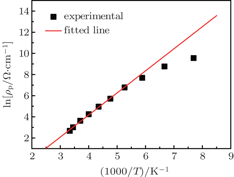
The carrier transport mechanism in the contact region of this sample could be studied from the sheet resistivity of samples (ρ p) as a function of temperature according to the I– V– T measurements, [14, 17, 18] where the resistivity ρ p(T) is derived from the sheet resistance, Rsh, of the sample obtained from the temperature-dependent CTLM measurements. We try to show an Arrhenius plot of ln(ρ p) ∼ 1/T for Sample A. It is found that the Arrhenius plot of ρ p for Sample A shows a significant deviation from the straight line, as shown in Fig. 1. It suggests that in this sample with p+ + -GaN contact layer, the conduction mechanism, in which the carriers are thermally activated and jump over a certain metal/semiconductor energy barrier (as in a normal Schottky barrier), is not the dominant one. Instead, the metal contact to ultra-highly Mg-doped p-GaN may be caused by variable-range hopping (VRH) conduction through the Mg-related deep-level defect (DLD) induced band. Actually, the variable-range hopping model was first proposed by Mott.[19] This model describes the conduction in strongly disordered systems with localized charge-carrier states, and the carrier’ s hopping to a state with higher energy is assumed to be a rate-limiting process. The probability of hopping between two neighboring states depends on their spatial separation and energy separation. If the VRH mechanism is valid, [11] then ρ p should follow a temperature dependence as ρ p ≈ exp(T0/T)1/4, where  kB is the Boltzmann constant, ND is the concentration of DLDs, and ad is the localization length.
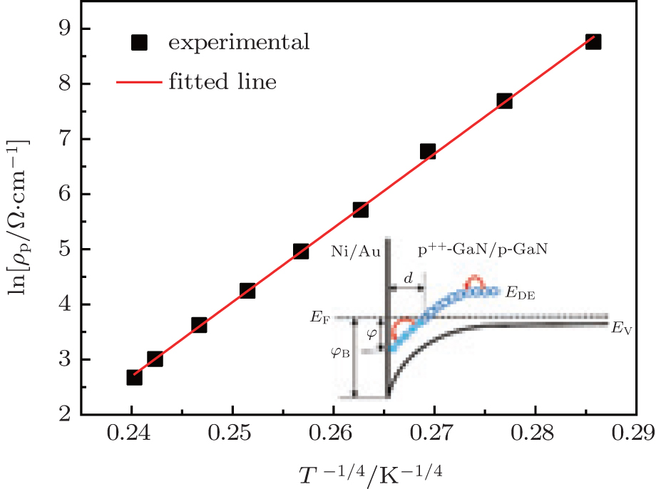
In order to check the conduction model, figure 2 is depicted to show a semi-logarithmic plot of ln(ρ p) as a function of T− 1 / 4. Note that the semi-logarithmic ln(ρ p) versus T− 1 / 4 curve for Sample A follows the straight line relationship reasonably well across the entire temperature range of 140– 320 K, as shown in Fig. 2. This constitutes essential evidence for VRH conduction through the DLD band in Sample A in the whole temperature range considered.
It is known that in heavily Mg-doped p-GaN layer, [Mg], i.e., the concentration of ionized Mg impurities, is limited by the high acceptor activation energy and the possible clustering of Mg atoms, being much less than the total concentration of Mg atoms. In fact, the excessive Mg will form the DLD band, [17, 20] which is schematically depicted in the energy diagram of Fig. 2 (cyanine circles in the inset). As shown in the inset of Fig. 2, the carriers will transport by the VRH conduction through the DLD band in Sample A. The height of the barrier that the transported carriers should overcome during the process is marked as φ . It is understood that the DLD band near the metal-semiconductor interface is bent downwards below the Fermi level with an energy separation of φ , which is much lower than the Schottky barrier height φ B, so the carriers can transport much easier by the VRH conduction through the DLD band, rather than jump over the Schottky barrier height. That is to say, the dominant carrier transport mechanism in Sample A and other samples with p+ + -GaN contact layer is VRH conduction through the DLD band, especially when the concentration of Mg and the thickness of the p+ + -GaN contact layer are suitable to form a proper DLD band.
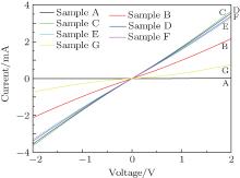
The influence of thickness of the p+ + -GaN layer on the performance of ohmic contact is studied next in detail. A series of samples named Sample A– G is examined in this experiment with different p+ + -GaN thickness in the range from 12 nm to 36 nm. The thickness is determined by the growth time. The other MOCVD growth conditions are the same for these Samples. For example, the growth temperature of MOCVD is fixed at 920 ° C and the Mg/Ga flow rate ratio is 8.35%. For all these samples, if there is no other special instruction, the rapid thermal annealing for alloying is processed in an oxidizing atmosphere at 550 ° C for 10 min.
Figure 3 shows the result of CTLM I– V measurement for the samples with different thickness of p+ + -GaN layer when the spacing d of the CTLM pattern is fixed as 30 μ m. As shown in Fig. 3, when the thickness of the p+ + -GaN layer is in the range from 21 nm to 27 nm, the CTLM I– V curves of contact to p-GaN show a linear relationship very well. However, the linear characteristic degrades with the decreasing of the layer thickness, in particular, the curves exhibit nonlinear characteristics when the thickness of the p+ + -GaN layer is thinner than 12 nm. Meanwhile, when the thickness of p+ + -GaN layer is thicker than 36 nm, the CTLM I– V curves also show nonlinear characteristics.
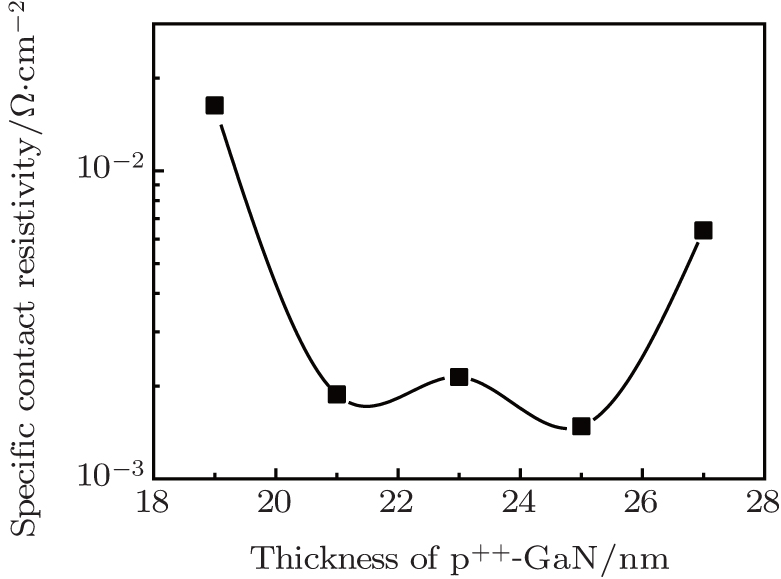
Figure 4 exhibits the specific contact resistivity (ρ c) as a function of the thickness of the p+ + -GaN layer in the range from 19 nm to 27 nm. Even though all of these 5 samples, including samples C and F, show linear characteristics in CTLM I– V curves, the ρ c values are below 2× 10− 3 Ω · cm2 only for Samples A, D, and E, as shown in Fig. 4. The ρ c values of samples C and F are relatively high. It is concluded that the optimal thickness of p+ + -GaN layer is in the range from 21 nm to 25 nm.
As reported by Figge et al., [21] it was found that the concentration of Mg in the contact layer is not homogeneous. Because the Mg concentration in this layer is much higher than that in the inner part of the p-GaN layer, the concentration of Mg rises gradually along the growth direction up to the surface. Thus, a certain thickness of the heavily Mg-doped GaN layer is required for keeping the concentration of Mg above the set value in the whole layer.[18] Then the proper DLD band can be produced, [22] and thus the ohmic contact to p-GaN can be obtained.[14, 17] This may be the reason why the samples B and C whose contact layers are very thin have a non-ohmic contact. In fact, if the contact layer is thinner than a certain thickness, for example, 21 nm for our samples, the concentration of Mg does not reach the set value and is too low to produce the DLD band, thus the contact quality is low. On the other hand, because of the poor material quality of the overly-thick heavily Mg-doped GaN layer, in general, the thicker the ultra-heavily doped layer, the more the defects and threading dislocation lines, then an increasing difficulty for carriers to transport through DLD bands by variable range hopping (VRH) conduction (which is assumed to be the dominant mechanism for very heavily doped p-GaN) will result in a degrading ohmic contact. In fact, the possibility for carriers to be captured during VRH conduction will increase because of poor material quality and a longer hopping distance. This can explain why the current of Sample G in Fig. 3 is relatively small. It is therefore concluded that the thickness of p+ + -GaN should be optimized. It should be thick enough to make the concentration of Mg reach the required set value, and at the same time it should be grown as thin as possible to make carrier transport easy.
Table 1.
Table 1.
 Table 1. Growth conditions of the p+ + -GaN layer for the samples used for the CTLM I– V measurements. The growth temperature of the p+ + -GaN layer for these samples is 920 ° C.| Sample | Cp2Mg flow rate | Flow rate ratio | Growth | ρ c/Ω · cm2 |
|---|
| /μ mol· min− 1 | (Mg:Ga) | thickness/nm | |
|---|
| H | 1.92 | 6.44% | 25 | 5.86× 10− 3 | | E | 2.49 | 8.35% | 25 | 1.48× 10− 3 | | I | 3.07 | 10.29% | 25 | 6.97× 10− 4 | | J | 3.76 | 12.60% | 25 | non-linear |
| Table 1. Growth conditions of the p+ + -GaN layer for the samples used for the CTLM I– V measurements. The growth temperature of the p+ + -GaN layer for these samples is 920 ° C. |
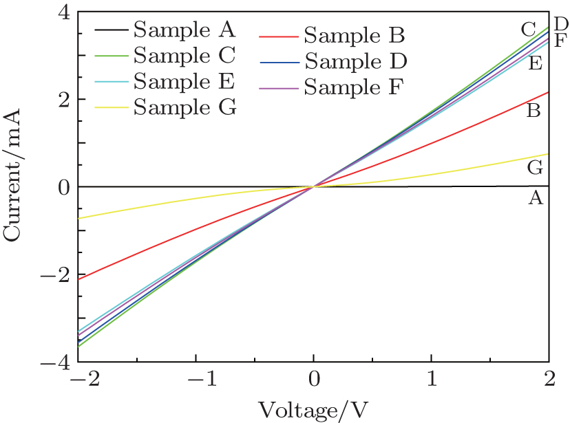
The influence of Mg/Ga flow ratio of the p+ + -GaN layer on the performance of ohmic contact is also studied. Four samples A, H, I, and J are grown with different concentration of Mg. The flow rate of Ga remains the same for Samples H, I, J, and A during the MOCVD growth, but the CP2Mg flow rate is different. The growth temperature was fixed at 920 ° C. Table 1 shows the growth conditions and ρ c of p+ + -GaN layer for the samples used for the CTLM I– V measurement. It is concluded that Sample I achieves the lowest ρ c in four samples when the Cp2Mg flow rate of p+ + -GaN layer growth is 3.07 μ mol/min and the Mg/Ga flow rate ratio is 10.29%.
Figure 5 displays the results of CTLM I– V measurement for four samples with different Cp2Mg flow rates when the spacing of the CTLM pattern is fixed at 30 μ m at room temperature. As shown in Fig. 5, the current increases along with the increase of Cp2Mg flow rate initally, but when the Cp2Mg flow rate increases to 3.76 μ mol/min for Sample J, the current decreases greatly, and the I– V curve shows a non-linear characteristic.
As shown in Fig. 5, the CTLM I– V characteristics of samples H, A, and I all show ohmic contact behaviors. The structure diagram of the optimal contact layer for Ni/Au ohmic contact to p-GaN studied in this part is shown in the inset of Fig. 5. The measured current at 2.0 V between two metal pads with a gap spacing of 30 μ m is 4.0 mA for Sample I, but the corresponding current values are only 2.4 mA and 3.3 mA for Samples H and A, respectively. The latter two samples are grown with Mg/Ga flow rate ratios lower than that of Sample I. The current of Sample I whose Cp2Mg flow rate during p+ + -GaN layer growth is 3.07 μ mol/min is the largest one of the three samples, and the ρ c value of Sample I is the lowest one, i.e., 6.97× 10− 4 Ω · cm2. It means that if the Cp2Mg flow rate of p+ + -GaN layer is less, the ρ c value has a trend to increase.
Kozodoy et al. showed that the excessive Mg could produce a deep-level defect (DLD) band in p-GaN only when the concentration of Mg doping is as high as 2.0× 1020 cm− 3, [23] which is in favor of obtaining a low contact resistance.[24] In this study, the SIMS measurement is made for Sample A and the result reveals that the total Mg impurity concentration in the p+ + -GaN layer is about 2.3× 1020 cm− 3. Hence, when the Cp2Mg flow rate is lower, the incorporated Mg concentration may also be lower, and the Mg-induced DLD band may not be well formed, or the density of states in the DLD band is not high enough to improve the carrier transport. This can explain why the ρ c of Samples H and A is higher than that of Sample I. In addition, when the Cp2Mg flow rate is too high, the material quality begins to strongly deteriorate and a severely degraded surface morphology consisting of densely packed hexagonal pyramids appears.[23] Therefore, when the Mg concentration of p+ + -GaN layer exceeds a certain value, the contact to p-GaN with p+ + -GaN contact layer may be degraded. That is the reason why the I– V curve of Sample J exhibits nonlinear characteristic when the Cp2Mg flow rate is raised to 3.76 μ mol/min. These results indicate that there is a suitable Mg concentration range of the p+ + -GaN layer for achieving excellent ohmic contact by producing an optimized DLD band.


 , Jiang De-Sheng