


Effects of tilt interface boundary on mechanical properties of Cu/Ni nanoscale metallic multilayer composites
[Yang Meng†a)  , Xu Jian-Gang
a) , Song Hai-Yang‡b) , Zhang Yun-Guanga) ]
, Xu Jian-Gang, Zhang Yun-Guang|
|


†Corresponding author. E-mail: ymphysics@163.com
‡Corresponding author. E-mail: gsfshy@sohu.com
*Project supported by the National Natural Science Foundation of China (Grant No. 10902083), the Program for New Century Excellent Talent in University of Ministry of Education of China (Grant No. NCET-12-1046), the Program for New Scientific and Technological Star of Shaanxi Province, China (Grant No. 2012KJXX-39), and the Natural Science Basic Research Plan in Shaanxi Province, China (Grant No. 2014JQ1036).
The effect of tilt interfaces and layer thickness of Cu/Ni multilayer nanowires on the deformation mechanism are investigated by molecular dynamics simulations. The results indicate that the plasticity of the sample with a 45° tilt angle is much better than the others. The yield stress is found to decrease with increasing the tilt angle and it reaches its lowest value at 33°. Then as the tilt angle continues to increase, the yield strength increases. Furthermore, the studies show that with the decrease of layer thickness, the yield strength gradually decreases. The study also reveals that these different deformation behaviors are associated with the glide of dislocation.
The interface, one of the most common microstructures found in solids, plays a vital role in contributing to various physical and chemical properties of material. So far, different types of metallic interfaces have been studied quite extensively, such as twin boundary (TB), [1, 2] grain boundary (GB), [3– 12] and nonmetal interface.[13] In particular, considerable attention has been focused on metal– metal interfaces.[14– 19] The structure of interface, [14, 15] and the interaction between dislocations and interfaces, [16– 19] govern the mechanical behaviors of nanoscale metallic multilayer composites (NMMCs). Most previous studies focused on the effects of interfaces on the mechanical behavior, there is limited work on studying the issues of tilt interface. Nevertheless, the crystalline orientation[20– 23] has a strong effect on the deformation mechanism. Zhang et al.[21] studied the TB migration and detwinning of low angle and high-angle planar twist TB in copper. You et al.[22] showed that the TB orientation effect of dislocation nucleation and propagation in nanotwinned metals. Fensin et al.[23] investigated the effect of grain boundary inclination with respect to the loading direction on void nucleation at a boundary. Such studies focused on tilt TB and GB properties of nano-materials, but the incline interfaces of NMMCs explored have still very rarely been studied.
NMMCs with various layer thickness values exhibit different deformation mechanisms. Abdolrahim et al.[24] investigated the deformation mechanisms of Cu/Nb nanowires with varying layer thickness under biaxial tensile loading. They revealed that the strength of smaller layer thickness is increasingly likely to be controlled by the nucleation of dislocations from the interfaces. Yuan and Wu[25] investigated the tensile deformation behaviors for two types of sub-10-nm multilayer nanowires in different layer thickness values by molecular dynamics (MD) simulations. It is found that the deformation mechanism changes from interface crossing by dislocations to interface rotation as the layer thickness decreases. Although most of the studies focused on the deformation behaviors of the NMMCs with different layer thicknesses, the tilt interface boundaries with different layer thickness have seldom been studied.
In the present paper, MD simulations are carried out to study the mechanical properties of Cu/Ni multilayer nanowires with different tilt interface boundaries and various layer thickness values. The simulation studies reveal that the crystalline orientation has strong effects on the deformation mechanism, and yield stress, demonstrating the importance of the slip systems within the multilayer nanowires for the incline interface. The fundamental mechanism responsible for changing the strength properties of NMMCs is also identified.
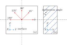
In order to study the effects of tilt grain boundary and layer thickness on tensile deformation mechanisms, we consider three sets of Cu/Ni multilayer nanowire samples, in which the interface boundaries are parallel, inclined and perpendicular to the loading orientation. The models are composed of two alternating phases Cu and Ni with a face centered cube (fcc) structure. Here, MD simulations are performed to study the mechanical properties of the types of NMMCs with twist boundaries under tension loading. The initial orientation of the Cu region (111) is the same as that of the Ni region, which is then anticlockwise rotated about the x axis by a different angle. We explore the case of six tilt angles, i.e., θ = 0° , 10° , 26.6° , 33° , 45° , and 90° as shown in Fig. 1. For the sample of 45° , the thickness h of each of the layers along the z axis varies between 1.88 nm and 6.88 nm in different simulations. The simulative sample of material has a free surface in the x and y directions and has a periodic boundary condition in the z direction. Uniaxial tension is applied along the z axis. All Cu/Ni samples have the same dimensions of 6.6 nm× 6.6 nm in x and y directions, respectively. The number of atoms in both samples ranges from 39728 to 145652.
 | Fig. 1. Illustration of the strategy of studying the effect of (a) crystallographic orientation and (b) inclination angle. |
The selection of the potential function is a vital factor which determines the accuracy of the results in MD simulation. Here, the embedded-atom-method (EAM) potential was developed for alloy by Zhou et al.[26] and Foiles.[27] This EAM potential is well fitted to basic material properties, such as lattice constants, elastic constants, bulk module, vacancy formation energies, sublimation energies, and heats of solution. A step of 2 fs is used in all MD simulations. The Nose– Hoover thermostats[28] at 0.01 K are used to control the system temperature. The samples are subjected to an applied constant strain of 0.001. During the simulation, the strain is applied by consistently adjusting the z coordinate of each atom according to the applied strain rate of 1.6 × 10⁸ s− 1.
In order to discern defects in the nanowires, colors are assigned to the atoms in the light of the local crystalline structure visualized by using common neighbor analysis (CNA).[29] This is implemented by using the open visualization tool (OVITO).[30] The analysis and classification of each atom according to its environment allow us to identify the various deformation mechanisms during tension loading. Here, the fcc, hexagonal close-packed (hcp) non-structured atoms (often existing in the free surface or at the dislocation core) are colored green, red and gray, respectively.
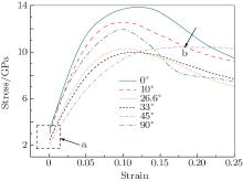
We first investigate the mechanical behaviors of the Cu/Ni NMMCs with various tilt angles. Figure 2 shows the classical stress-strain curves of the corresponding loading for different tilt angles. It can be observed from Fig. 2 that for θ = 0° , the yield stress is highest. For θ > 0° , the yield stress decreases with increasing degree, until it reaches 33° and then it continuously increases. Meanwhile, the curve of 45° displays an increase in stress with increasing strain until the yield strain, followed by fluctuations around the critical stress, implying that the plastic response of 45° is much better than the other samples. It can be seen from Fig. 2 that there are finite initial stresses in the “ a” region, although the samples are relaxed adequately before tensile loading. This is mainly because the interfacial and surface stress cause an intrinsic compressive stress in the interior of the nanoscale metallic multilayer composites, and the compressive stress should be overcome by a stress at the initial moment of the tensile loading process. In addition, figure 2 shows that the Young’ s modulus of the Cu/Ni nanoscale metallic multilayer composites slightly decreases with increasing twist angle. It can be explained that for an fcc crystal, E(100) < E(110) < E(111), [31, 32] which means that the Young’ s modulus reaches a maximum value in 〈 111〉 and a minimum value in 〈 100〉 . For the sample with a relatively low tilt angle (for example 10° ), the crystalline orientation almost does not deviate from the (111) plane, while for high twist angle (for example 45° ), the crystalline orientation deviates from the (111) plane severely. Hence, the Young’ s modulus decreases with the twist angle increasing from 0° to 45° .
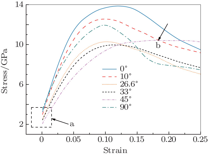 | Fig. 2. Typical stress– strain curves for the Cu/Ni multilayer nanowires in different angles under tension loading. |
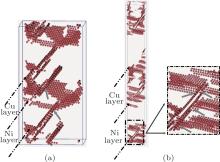
To reveal the deformation mechanisms for the sample at various angles under uniaxial loading, the dynamic evolution of the dislocation is analyzed. Figure 3 shows the atomic configurations of Cu/Ni multilayer nanowires with 0° and 33° at different strains of loading. In the case of θ = 0° , the first dislocation nucleates from the ledge of the surface in the softer layer that is Cu in this case as shown in Fig. 3(a). Hence, the crystal structure of the Ni layer is still nearly perfect without lattice defect. After nucleation, the dislocations propagate toward the Cu layer interiors along 〈 111〉 . As the sample is further loaded to 0.12 strains, multiple slip systems are activated in the layer, and the dislocations intersect and cross over each other, thus enhancing the hardening effect, and strengthening the nanowires. In the case of θ = 33° , the dislocation emits from the surface of the Cu layer, and travels along a slip plane until it reaches the interface. With continuing to load, two slip systems are activated and dislocations with less different slip systems may intersect and cross with each other, thus leading to the softening behavior of material as seen in Fig. 3(b). The strength of material is controlled by dislocation interactions.
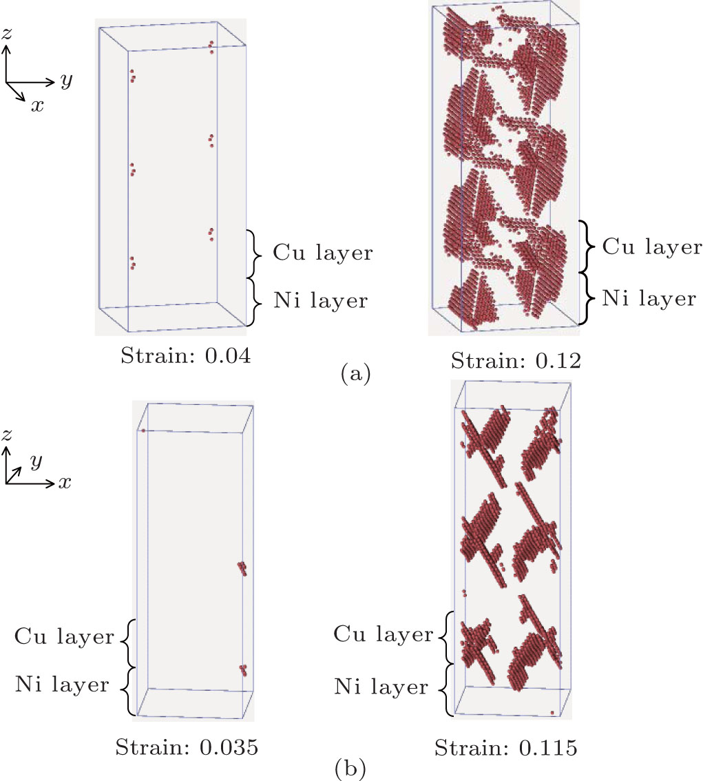 | Fig. 3. Atomic configurations with different twist angles: (a) the Cu/Ni nanoscale metallic multilayer composites with a twist angle of 0° under different tension strains of 0.04 and 0.12; (b) Cu/Ni nanoscale metallic multilayer composites with a twist angle of 33° under different tension strains of 0.035 and 0.115. Atoms are colored by using a common neighbor analysis method (hcp in red). |
Figure 2 shows that the model of 45° displays excellent plasticity response. For comparison, the atomic configurations of 45° and 10° tilt angle modes at the same strain levels are also shown in Figs. 4(a) and 4(b), respectively. Under 45° tension, most partial dislocations nucleate in the intersection region of the interface and surface in the initial stage, and glide on the interface planes, on the layer with the fewest defects as shown in Fig. 4(a). As the loading increases, the interface migration resulting from partial dislocation gliding on interface planes (see Fig. 4(a)) plays an important role in the plastic deformation.[21, 33] In contrast, for the case of 10° , plenty of intersecting dislocations and interface planes are observed; a higher density of stored dislocations than that for the 45° case is shown in Fig. 4(b). This difference is caused by the crystalline orientation that dominates each of the slip systems.[18] In the case of 45° , the favorable slip systems are coplanar with the interface, the slip directions are parallel to the interface and hence dislocations intersecting with interface planes are rarely seen here. Therefore, the slip system leads to the decrease of dislocation pileup near the interface, which reduces the stress concentration to a large extent, thus leading to the increase in plasticity of material. In the 10° case, the slip plane and the slip direction of the active slip system incline to interface, thereby inducing the dislocation– dislocation and dislocation– interface interaction. From Fig. 4(b), numerous dislocations pile up and interaction induces a large material potential energy, which hinders the plastic deformation of material.
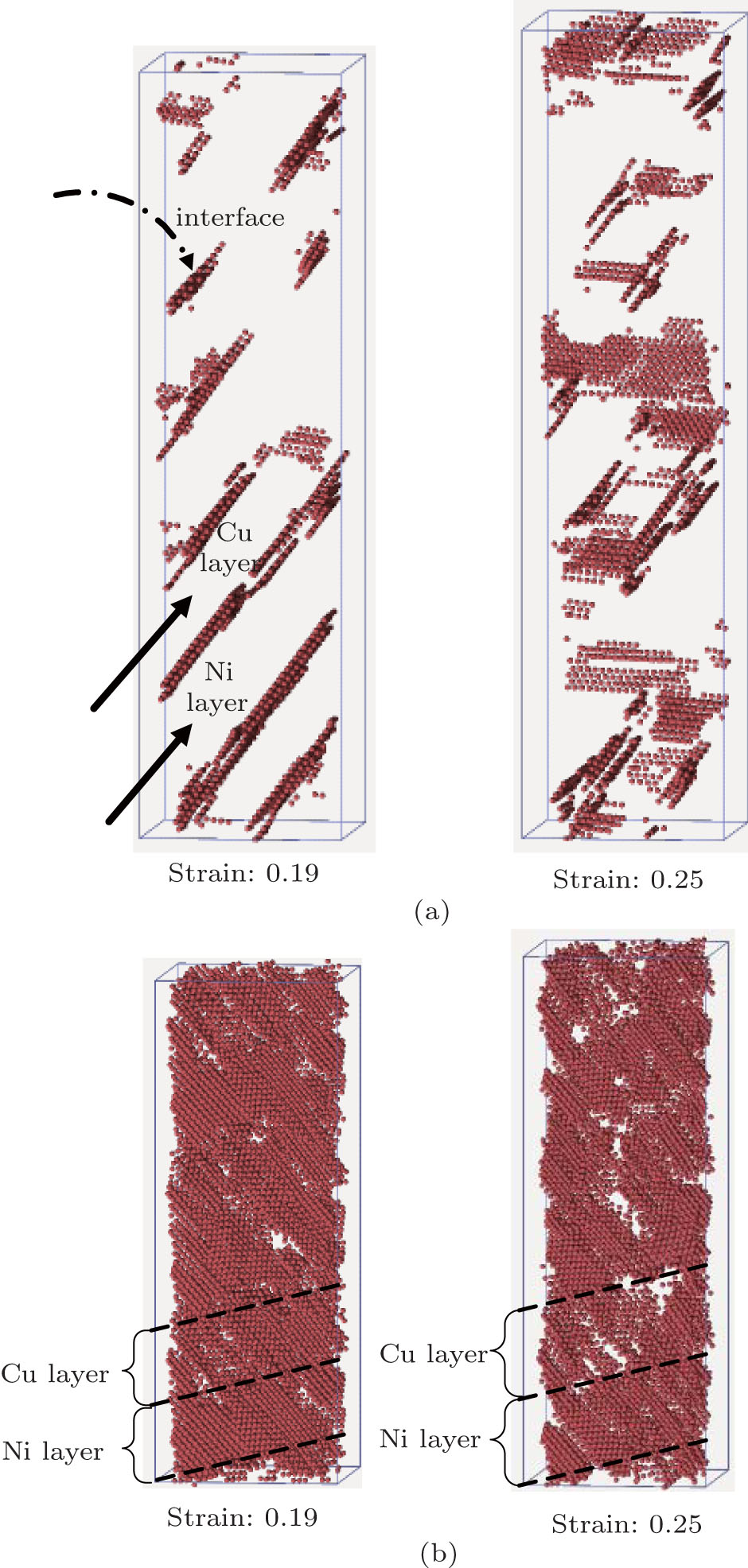 | Fig. 4. Atomic structure configurations of Cu/Ni with tilt angle θ = 45° (a) and θ = 10° (b) at the same strain levels. |
In order to understand the underlying mechanism of the 45° , we also investigate the deformation behaviors of the structure with different layer thickness values. Figure 5 shows the stress– strain curves for NMMCs with layer thickness (h) values of about 1.88 nm, 3.76 nm, 5.01 nm, and 6.98 nm. From Fig. 5, we can find that the Cu/Ni NMMCs with 45° tilt angle displays excellent plasticity, regardless of layer thickness. This result indicates that the twist interface plays an important role in determining the plasticity properties of Cu/Ni nanowires. It can also be seen from Fig. 5 that the effect of layer thickness on the Young’ s modulus is very slight, the same as that in the 45° case. In addition, the simulation result indicates that the yield strength can be evidently enhanced with increasing layer thickness. Thus there may exist a reversal of the Hall– Petch (HP, the smaller grain size, the higher strength) effect. This is consistent with the conclusion obtained by Yuan and Wu[25] in Cu/Ag multilayer nanowires. To further understand the deformation mechanism, the atomic structures of Cu/Ni nanowire with layer thickness values of 1.88 nm and 6.98 nm under the critical strain are shown in Figs. 6(a) and 6(b), respectively. For the nanowire sample with a larger thickness value, there will be more storage room for dislocations. As the storage room is too small for dislocations to pile-up inside the lattice, the mechanical properties will be very limited. It follows from Fig. 6 that the capacity of material for dislocation storage with a layer thickness of 1.88 nm is obviously lower than that with a layer thickness of 6.98 nm. Furthermore, the dislocation storage capacity of NMMC does not increase with increasing layer thickness when layer thickness is larger than 5.01 nm, and the material properties change slightly. The result is mainly due to the fact that the magnitude of the repulsive force and the room for dislocation storage can be affected by the change of layer thickness.[1]
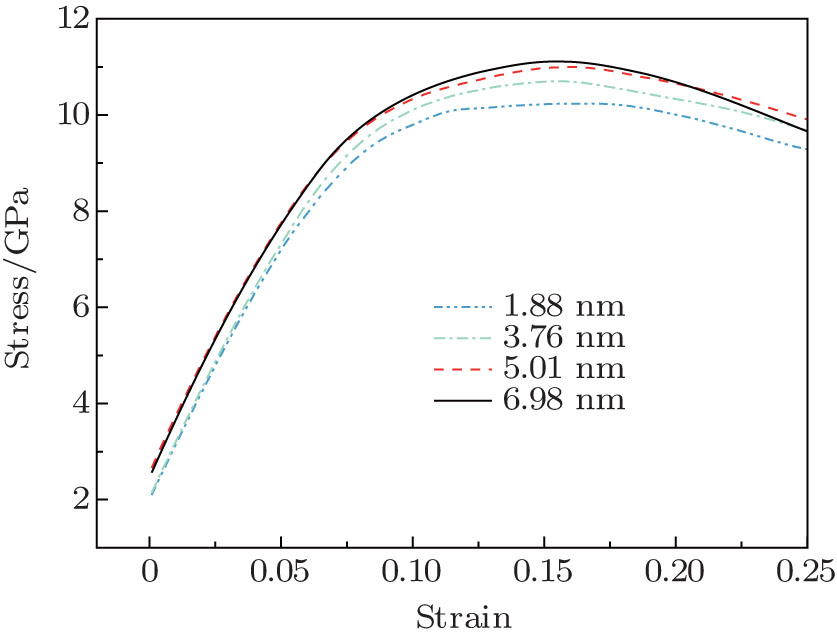 | Fig. 5. Typical stress– strain curves for the samples of 45° with different layer thickness values under tension loading. |
 | Fig. 6. Atomic structure configurations of Cu/Ni with layer thickness (a) h = 1.88 nm and (b) 6.98 nm under their corresponding critical stresses. Arrows show the interactions of dislocations in different slip planes. |
Subsequently, we analyze the microscopic structure. Figure 6(a) shows partial dislocations nucleated from the intersections of the free surface and interface plane and moves in the direction parallel to the interface in the case of h = 1.88 nm at the yield point. Owing to the confinement imposed by the small size layers, there is limited room for the dislocations to move along the slip plane, leading to most dislocations being parallel to the interface, and rarely being seen to intersect with the interface plane. In contrast, when the layer thickness becomes 6.98 nm, figure 6(b) shows that more dislocations nucleate from the interface in the Cu layer, thereby activating the different slip systems, and dislocations interact more with each other, resulting in the highest yield stress. This result is in agreement with a previous atomistic result, [24] where it is shown that the slip systems improve the properties of the material.
The deformation behaviors of nanoscale metallic multilayer with different tilt angles and layer thickness values are studied using MD simulation method. This work reveals that crystalline orientation has strong effects on plastic deformation and yield stress, demonstrating the importance of the slip system in the multilayer nanowires for the tilt interface. In the case of θ = 45° , the plastic response is much more than the others, which may be explained by the dislocation nucleation and the effect of the slip system. For θ = 0° , the yield stress is highest; for θ > 0° , the yield stress decreases with increasing the value of θ ; the yield stress is the lowest at about θ = 33° and then increases. With the increase of the layer thickness, the strength always increases, thus there may exist a reversal of the HP effect. The material with a thick layer is obviously effective for the dislocation storage. The general conclusions derived from this work may provide a guideline for the design of high-performance Cu/Ni nanoscale metallic multilayer composites.
| 1 |
|
| 2 |
|
| 3 |
|
| 4 |
|
| 5 |
|
| 6 |
|
| 7 |
|
| 8 |
|
| 9 |
|
| 10 |
|
| 11 |
|
| 12 |
|
| 13 |
|
| 14 |
|
| 15 |
|
| 16 |
|
| 17 |
|
| 18 |
|
| 19 |
|
| 20 |
|
| 21 |
|
| 22 |
|
| 23 |
|
| 24 |
|
| 25 |
|
| 26 |
|
| 27 |
|
| 28 |
|
| 29 |
|
| 30 |
|
| 31 |
|
| 32 |
|
| 33 |
|