Effects of back gate bias on radio-frequency performance in partially depleted silicon-on-inslator nMOSFETs
Shanghai Institute of Microsystem and Information Technology, Chinese Academy of Sciences, Shanghai 200050, China
†Corresponding author. E-mail: jchen@mail.sim.ac.cn
1. IntroductionSilicon-on-insulator (SOI) technology has been considered as a potential technology for high frequency application due to the high cut-off frequency, which has already reached to 500 GHz, and also for the harsh environment, such as high temperature and radiation environment.[1] Although SOI metal-oxide semiconductor field-effect transistors (MOSFETs) suffer floating body effect (FBE) caused by impact-ionization which restricts the application in analog integrated circuits, the body contacts with different structures are investigated to suppress FBE, such as T-gate (TB), H-gate, body-tied-source, etc. As we previously reported, [2] tunnel diode body-contact (TDBC) structures suppress the FBE successfully without adding additional parasitics compared with the conventional body-contact structures. TDBC structure could also achieve a similar cut-off frequency (fT) and even better maximum frequency of oscillation (fmax) due to smaller parasitic gate– source capacitance.
In general, the effect of back gate bias (BGEs) of the N-type MOSFET in partially depleted (PD) SOI is very small and it is always ignored. However, it has been reported that with the decreasing of the buried oxide thickness (box), the penetration of electric field from the source/drain region into the body via the box decreases, thus enhancing the immunity to short channel effect (SCE), [3] and improving the heat dissipation ability.[4] However the characteristics become sensitive to the back gate bias (VBG) in PD SOI MOSFET, and the influences of VBG on DIBL, [5] hysteresis effect, [6] and carrier mobility[7] have recently been investigated. In this paper, BGEs on RF performance in PD SOI nMOSFETs are investigated experimentally.
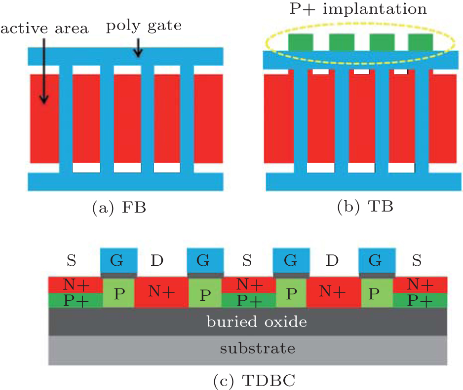
2. Devices and measurementThe RF performances of three different types of transistors of which supply voltages are all 1.2 V are investigated by applying various values of VBG, namely 1) floating body (FB), 2) T-gate body-contact (TB), and 3) tunnel diode body-contact (TDBC). All of the devices are fabricated by using the 0.13-μ m PD SOI CMOS technology. The devices investigated in this paper have the same dimensions. The devices are designed with multi-fingers with the same gate length, 0.13 μ m and total width, 40 μ m. The finger width, finger number are 2 μ m and 20 respectively. The gate oxide, top silicon, buried oxide thickness are 1.8 nm, 100 nm, and 145 nm. For each FB device and TDBC device, the gate is contacted from both sides to reduce the parasitic gate resistance. TB device is designed to contact from only one side due to design rule limiting, which could result in a higher value of gate resistance. The difference between FB and TDBC devices is that for the TDBC device one Esaki diode[8] is embedded in the source region to suppress the floating body effect. Fabrication procedure can be found in Ref. [9]. For the TB device, P+ implantation is performed to form the P+ body contact area. Poly in the body-contact side is designed to separate the P+ implantation area from source/drain area. The top view of FB and TB devices are shown in Figs. 1(a) and 1(b), and the cross-section view of TDBC is shown in Fig. 1(c).
To investigate the BGEs on the RF performance, two-port S-parameters under different VBG values are measured with frequency varying from 0.1 GHz to 30 GHz in steps of 100 MHz. The VBG varies from − 20 V to 50 V. Open and short de-embedding method is used to assess the practical performance of these devices. All of the measurements are made with an Agilent B1500 and Agilent PNA-X N5244A with a Cascade Summit 12000M probe station.
3. Results and discussionThe fT and fmax are the key parameters for evaluating the RF performance of transistors.[10] The fT is the frequency when the drain current gain is unity, and fmax is the frequency when the power gain is unity. The fT could be extracted by the equation f0 × ∣ H21∣ and fmax could be obtained from  , where f0 is the applied transport frequency, H21 is the current gain, and MUG is the Manson’ s unilateral power gain. For the physics background, fT and fmax can be expressed as in the following equations:[11]
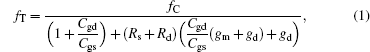
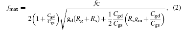
where fC = gm/2π Cgs represents the intrinsic cut-off frequency; gd is the output conductance for DC case; gm is the trans-conductance for low frequency; Cgs is gate-to-source capacitance; Cgd is gate-to-drain capacitance; and, Rg, Rs, Rd are gate resistance, source resistance, and drain resistance, respectively.
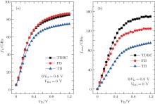
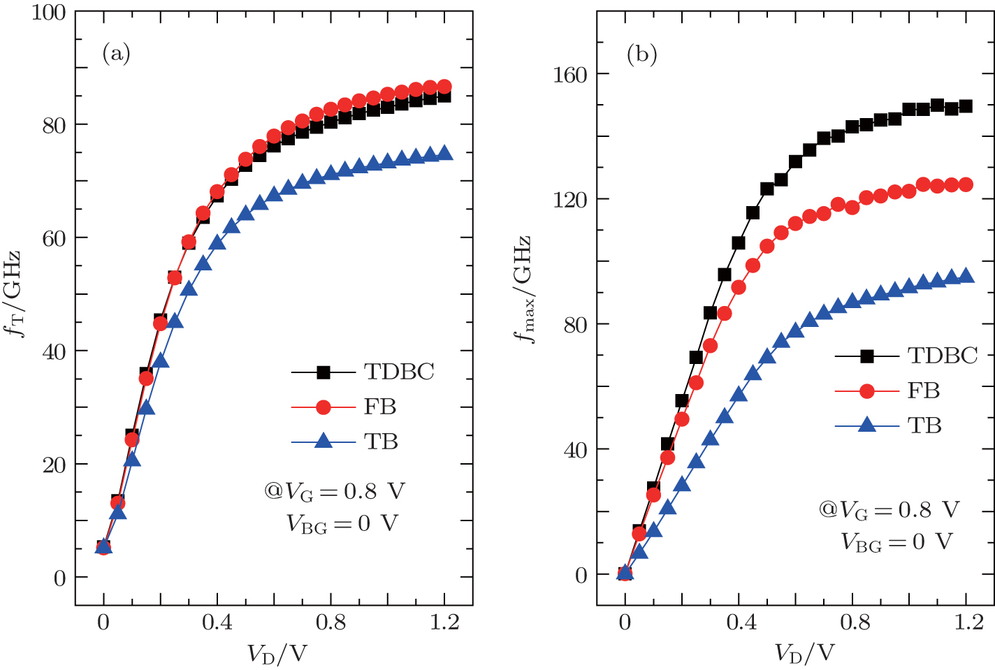
S-parameter under zero back gate bias is performed to extract the fT and fmax when the back gate bias is zero. Figure 2 shows the variations of fT and fmax with drain voltage at VG = 0.8 V and VBG = 0 V. From Fig. 2(a), fT of TDBC reaches 85 GHz when drain voltage is 1.2 V, similar to that of FB, 87 GHz. The reason for fT of TDBC lower than that FB is that the threshold voltage of TDBC is higher than that of FB device. The fT of TB device is 74 GHz when VD = 1.2 V, 13% lower than that of TDBC device due to the higher parasitic capacitance. Owing to the lower parasitic resistance and parasitic, fmax of TDBC could reach 150 GHz, ∼ 20% higher than that of FB, 125 GHz and ∼ 58% higher than that of TB, 95 GHz.
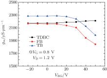
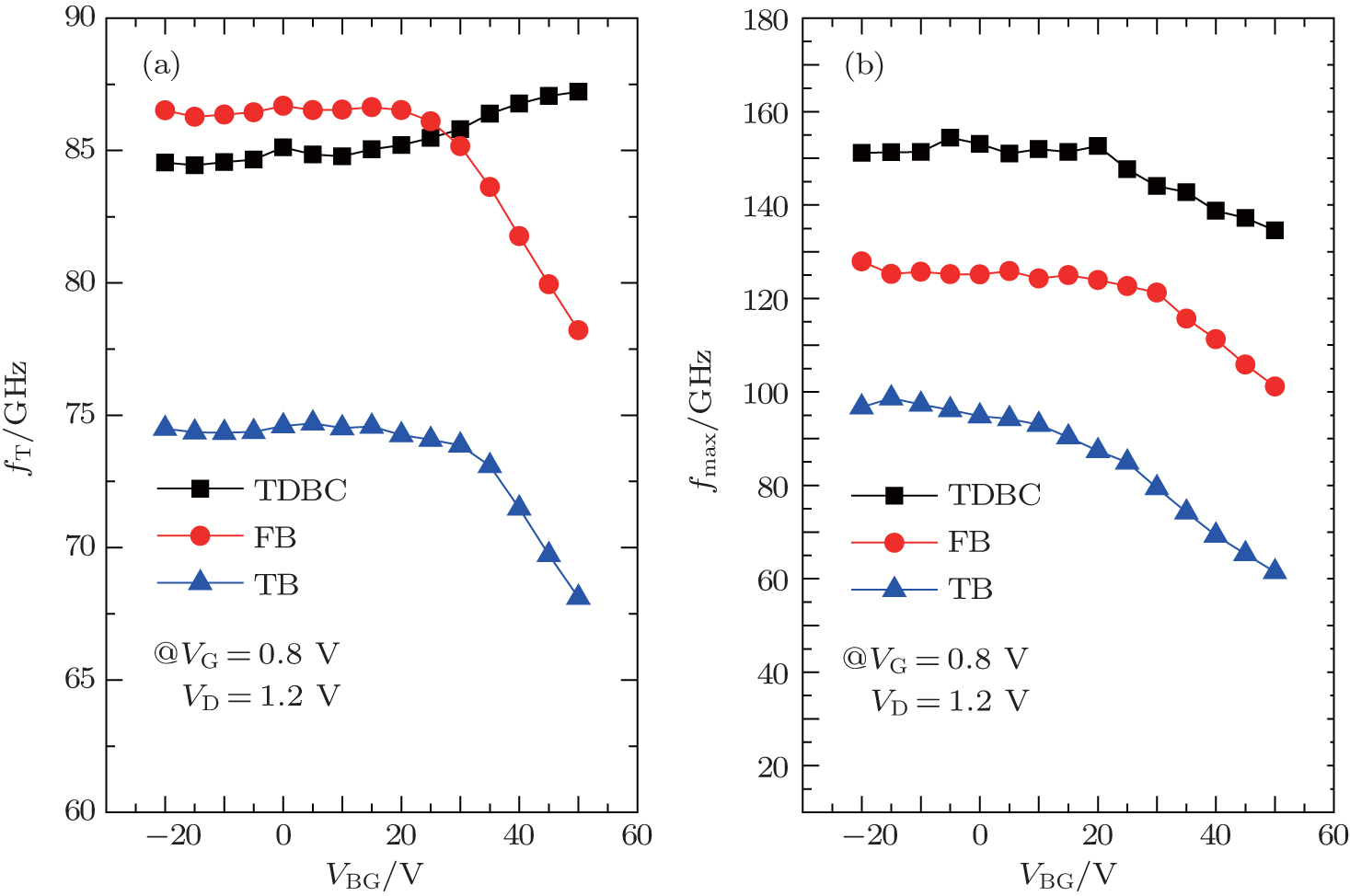
To perform the influence of back gate bias for different devices, S-parameters are measured under VBG values ranging from − 20 V to 50 V. The values of fT and fmax are obtained to evaluate the BGEs of different devices. Figure 3 shows that fT and fmax each behave as a function of VBG when VG = 0.8 V and VD = 1.2 V. The negative back gate bias has little influence on fT and always keeps a same value under zero back gate bias. While the fT values of FB and TB each have a significant degradation when VBG is larger than ∼ 20V. The reason for the degradation is that the transconductance (gm) degrades when the inversion appears between silicon and buried oxide. Unlike the behaviors of FB and TB, the fT value of TDBC slightly increases as VBG rises. Figure 4 shows the influences of VBG on gm of the three devices. As VBG increases, the gm values of FB and TB devices reduce after ∼ 20 V, while the gm value of TDBC slightly increases. When the VBG is positive and large enough, the inversion layer forms and the gate faces increase difficulty in modulating the new deep lying electron conducting paths between source and drain in FB and TB devices.[12] However, due to the existence of a P+ region under the source, it is difficult to form a conducting channel between the source and the drain. As a result, the gm values of TDBC devices almost remains the same.
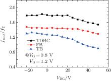
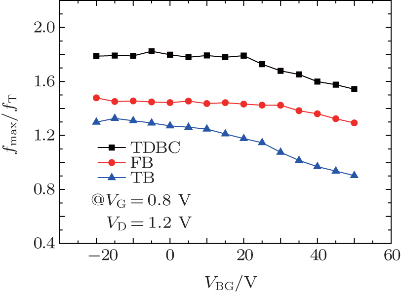
It is demonstrated that the degradation for fmax of MOSFET is mainly related to the decrease of Cgs/Cgd ratio and the increase of gd.[13] Figure 5 shows the comparison of the ratio of fmax to fT among the three different devices when VG= 0.8 V and VD= 1.2 V. The fmax / fT value of TDBC reaches 1.8 when back gate bias is zero, ∼ 25% higher than that of FB device, 1.44 and ∼ 42% higher than that of TB device, 1.27. However, the fmax / fT ratio decreases when VBG is positive. For FB and TB devices, the reason for reducing the ratio is the decreasing gm and increasing gd, as shown in Fig. 3 and Fig. 5. For the TDBC device, the gm is almost constant as VBG increases, and Cgs and Cgd are also independent of VBG. As a result, the intrinsic cut-off frequency, fC, almost has no dependence on VBG for TDBC. The decreasing of the ratio for TDBC mainly happens because of the degradation of gd and the slight increase of fT.
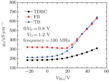
The gd is an important parameter for MOSFETs in microwave application because it has a significant effect on the fmax, as indicated in Eq. (2). Figu.re 6 shows the gd values of TDBC, FB and TB devices with VBG when frequency is 100 MHz where gd can be extract by Re (Y22). Due to the inversion layer between box and silicon, which could connect the drain and source when VBG is larger than ∼ 20V, the gd degradation slopes of FB and TB devices are 10.5 μ S/(μ S· V) and 12 μ S/(μ S· V), respectively. However, due to the lack of a back gate channel, the gd value of TDBC shows less degradation than those of FB and TB devices. The gd degradation of TDBC is only 3.35 μ S/(μ S· V), 68% lower than that of FB device, and 72% lower than that of TB device. The results show that BGEs of TDBC is much smaller than those of FB and TB.
4. ConclusionsTo investigate the influence of back gate bias on RF performance in PD SOI MOSFETs, different figures of merit are extracted under different back gate biases. The values of fT and fmax of TDBC reported in this paper reach 75 GHz and 150 GHz, respectively. Back gate bias has a significant influence on RF performances in FB and TB devices while it has less effects on the RF performance of the TDBC device. The fT value of TDBC shows scarcely the dependence on VBG while the fmax value of TDBC shows a slight dependence on VBG due to the degradation of gd. The fmax / fT ratios are also compared among the three types of devices, and the results show that the TDBC devices have a higher fmax / fT ratio than the others. High positive back gate bias can cause the gm values of FB and TB to decrease because of the emergence of strong inversion layer connecting the source and drain. The gd degradation of TDBC caused by back gate bias is much lower than those of FB and TB devices because of the absence of a back gate conducting channel. The results indicate that TDBC structure could effectively improve the BGEs in PD SOI NMOSFETs.


 , Luo Jie-Xin, He Wei-Wei, Huang Jian-Qiang, Chai Zhan, Wang Xi]