


Switching mechanism for TiO2 memristor and quantitative analysis of exponential model parameters
[Wang Xiao-Ping†a), b)  , Chen Min
a), b) , Shen Yia), b) ]
, Chen Min|
|


†Corresponding author. E-mail: wangxiaoping@hust.edu.cn
*Project supported by the National Natural Science Foundation of China (Grant Nos. 61374150 and 61374171), the State Key Program of the National Natural Science Foundation of China (Grant No. 61134012), the National Basic Research Program of China (Grant No. 2011CB710606), and the Fundamental Research Funds for the Central Universities, China (Grant No. 2013TS126).
The memristor, as the fourth basic circuit element, has drawn worldwide attention since its physical implementation was released by HP Labs in 2008. However, at the nano-scale, there are many difficulties for memristor physical realization. So a better understanding and analysis of a good model will help us to study the characteristics of a memristor. In this paper, we analyze a possible mechanism for the switching behavior of a memristor with a Pt/TiO2/Pt structure, and explain the changes of electronic barrier at the interface of Pt/TiO2. Then, a quantitative analysis about each parameter in the exponential model of memristor is conducted based on the calculation results. The analysis results are validated by simulation results. The efforts made in this paper will provide researchers with theoretical guidance on choosing appropriate values for ( α, β, χ, γ) in this exponential model.
The memristor postulated in classical papers by Dr. Leon Chua in 1971[1] and 1976[2] as the fourth basic circuit element has spurred a great deal of research interest since its physical implementation was released by HP Labs in 2008.[3] Chua also proposed how to recognize a memristor from its electrical properties.[4, 5] Nowadays, only a few groups can fabricate a memristor which satisfies these electrical properties, and most researchers still use mathematical models and physical theory to carry on their study by theoretical analysis and simulation.[6– 10]
To date, a large number of mathematical models have appeared.[11– 26] Many models are based on modeling equations proposed by HP Labs, which approximate the kinetic behavior of intrinsic dopants of the memristor in linear[3] and nonlinear manners.[11– 13] In addition, advances in memristor modeling have been discussed, including a model incorporating an exponential ionic drift equation, which was used to model oxygen vacancy movement, [14] a model correlating more closely to physical characterization data, [15– 17] a hyperbolic sine model, [15, 18– 22] approximating the metal– insulator– metal (MIM) tunnel junction, [23] a model using an ideal closed-loop operational amplifier, [24] a model based on a light-dependent resistor, [25] and the threshold flux-controlled memristor model.[26] However, these published models have failed to accurately describe the relationship between the model parameters and the mechanism of the switching behavior, which is meaningful for the future research of the memristor’ s application in various areas of electrical technology.
In this paper, we suggest a mechanism for switching behavior of Pt/TiO2/Pt structure introduced in Ref. [27], and discuss the parameters of the exponential model proposed in Ref. [14]. Then, an in-depth understanding of the switching mechanism and exponential model is achieved. Additionally, based on the switching mechanism, we quantitatively analyze the effect of each parameter in the exponential model of the memristor’ s characteristics, which can provide a theoretical reference to researchers on how to choose the appropriate parameters in the exponential model.
The rest of this paper is organized as follows. Section 2 illustrates the mechanism for the switching behavior of TiO2 memristor. In Section 3, we analyze the correlation between the parameters (α , β , χ , γ ) in the exponential model and the physical realization of memristors, and give the simulation results. Finally, our conclusions are drawn in Section 4.
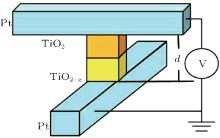
The physical structure of memristor was released by HP Labs in 2008, as shown in Fig. 1, the upper layer is composed of stoichiometric titanium dioxide, which is an electrical insulator. In contrast, the bottom layer is doped with oxygen vacancies, which makes this layer a conductor.[3] Due to the difference of work function between metal and metal oxide, the Schottky barrier is formed at the interface between metal and insulator. In the bottom layer, the high concentration of oxygen vacancies serves to collapse the Schottky barrier, and the Ohmic contact is produced at the interface of Pt/TiO2− x. In the upper layer, the low concentration of oxygen vacancies maintains the Schottky barrier at the interface of Pt/TiO2.
 | Fig. 1. The structure of Pt/TiO2/Pt memristor.[27] |
With an external electrical field, the positively charged vacancies drift in the given direction. The positive voltage can make the vacancies drift to TiO2 layer, then the Schottky barrier at the interface of Pt/TiO2 becomes an Ohmic contact and the memristor is switched to the ON state. When a negative voltage is applied to memristor, the vacancies in the conducting channel are repelled away from TiO2 layer and the original Schottky barrier is regained and the memristor is switched to the OFF state. This is suggested to be an example of bipolar switching, in which the ON and OFF states are switched with opposite bias polarity. This switching mechanism is inspired by valence-change, as illustrated in Ref. [28].
When a voltage is applied to the top electrode in Fig. 1, the positively charged vacancies in the oxide drift to the undoped TiO2 layer and result in an increase in the doping concentration of the TiO2 layer, which in turn makes the Schottky barrier width at the interface of Pt/TiO2 narrow. Based on the principle of quantum tunnelling, [19] when the barrier is as thin as the De Borglie wave length of electron (now the barrier is quantum barrier, the electron can tunnel through the barrier by electron wave property), the electron can tunnel through the barrier easily in the channels formed by the drift of oxygen vacancies and then the device is switched ON.
Supposing that the Schottky barrier is formed by a barrier of height Φ B and half width a. The barrier height Φ B is the difference between metal work function Wm and semiconductor electron affinity qχ [29, 30]

The electron affinity qχ is measured from the bottom of conduction band Ec to the vacuum level

where Ws is the work function of semiconductor, EF is the Fermi energy level of semiconductor, and Ec is the bottom of conduction band level. So the barrier height Φ B can be given by

And the barrier height of semiconductor is

The barrier height is associated with the material, the relationship between the barrier height Φ B and the barrier width XD is

where q is electronic charge (q = 1.6× 10− 19 C), ε 0 is the permittivity of vacuum, ε r is the relative dielectric constant of TiO2, ND is the concentration of vacancies in semiconductor. Without the external bias voltage, the probability of an electron jumping the barrier is
where v is the probability of electron transition without the barrier, k0 is Boltzmann constant, and T is temperature.
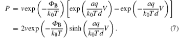
With the external field, electrons drifting from semiconductor to metal will be aided, while it will be opposed from metal to semiconductor. This effect is equal to replacing the effective barrier by Φ B− aqV/d coincided with the direction of the external field, and Φ B+ aqV/d opposite to the direction of the external field[14, 31] when the thickness of oxide layer is d. Therefore, the probability of an electron jumping the barrier can be concluded as
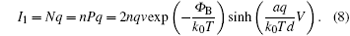
Consequently, when n electrons are available to carry the current, the number N electrons which can jump the barrier can be obtained by N = nP. So the tunneling current from semiconductor to metal can be given by multiplying electronic charge q by N
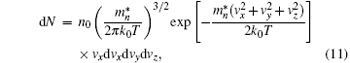
When a voltage V is applied to the top electrode, the vacancies in the conducting channel are repelled away from the top interface and the original Schottky barrier is regained. Based on the thermionic emission theory, [32] just like how electrons in metal pass through the potential energy barrier into semiconductor, the electrons in the semiconductor can penetrate into the metal layer as long as they have sufficient energies to overcome the potential barrier. We can calculate the current from semiconductor to metal by multiplying the number of electrons per unit volume which can hop the barrier by electronic charge q. The velocity of electrons is resolved into its three components vx, vy, vz, with the x-axis parallelling to the transport direction, namely from semiconductor to metal. The number of electrons in per unit volume is

where n0 is concentration of electrons in the conduction band in thermal equilibrium

In per unit electrode area, when the volume is equal to vx, the number of electrons which can arrive at the interface between metal and semiconductor in per unit time is
where 

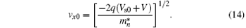
If Vs0+ V < 0, the electrons which can penetrate the barrier must satisfy the following condition:

The minimum velocity required in the x-direction is vx0
Because there is no exist barrier in the y-direction and in the z-direction, neither of the velocities in these two directions are limited. Current can be obtained by multiplying electron number N by electron charge q, so the current density formed by the electrons from semiconductor to metal is
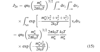
By substituting Eqs. (10), (12), (14) into Eq. (15), we get

and

A* is the effective Richardson constant for thermionic emission.[33]
The electrons in the metal are distributed in less than 0.1-nm film, while the thickness of the space charge layer (the electrons at the semiconductor surface) in a semiconductor is usually at the micron level. Therefore, the potential change caused by external voltage mainly concentrates in the semiconductor. The barrier height from metal into semiconductor remains the same. Therefore, the current density J2b formed by the electrons from metal to semiconductor remains constant, which equals to the current flowing from the semiconductor into the metal when thermal equilibrium prevails; i.e., when V = 0. This corresponding current density is obtained from Eq. (16) by setting V = 0,
Supposing the area of electrode is S, so the total current is given by
The tunneling current and the thermionic emission current exist simultaneously. It is important which one is at the leading position. So the current through the memristor is the sum of tunneling current and thermionic emission current:

Yang et al.[27] used the following model to describe the I− V switching characteristics of the memristor. This model can reproduce the I– V characteristics and has been widely used to model the physical structure of memristor

where ω is the state variable of memristor, and is normalized to [0, 1]. When the memristor is in the ON state, ω is close to 1 and ω n is close to 1, the current is dominated by the first term in Eq. (21). When the memristor is in the OFF state, ω is close to 0 and ω n is close to 0, the current is dominated by the second term in Eq. (21). The exponent n determines the effect of ω on the I– V curve. For the simplicity, the parameters (α , β , χ , γ ) are mainly discussed in this paper.
Remark 1 Yang et al.[27] suggested that the parameters (α , β , χ , γ ) were fitting constants, dimensionless, and depended on physical properties of the material of memristor. Next, the model equation (21) is compared with theoretical derivation expression (20). A quantitative analysis about the parameters (α , β , χ , γ ) effect on the I– V characteristic of memristor is conducted from a physical point of view.
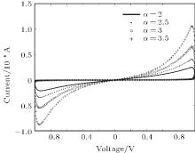
In this section, we use the model (21) and establish the HSPICE code to analyze qualitatively each parameter’ s effect on the properties of the memristor and discuss the reasons causing the phenomenon. We call the part with big current values “ low resistance” (Rlow) and that with small current values “ high resistance” (Rhigh). On the condition that the input signal is ideal sinusoidal signal with the frequency 1 kHz and the amplitude 1 V, the I– V characteristic curves of memristor become a twisted hysteresis. The high resistance Rhigh and the low resistance Rlow are measured with a voltage 0.7 V. At the same time, the I– V characteristics of the memristor are also discussed with applied voltage of different frequency.
The first term in Eq. (21) represents the tunneling current produced by the electrons tunneling through barrier when the memristor is in ON state. From Eq. (8), the parameter α is

Given the material of memristor, the parameter α is only associated with the half width of barrier a. According to Eq. (5), the parameter α is proportional to 
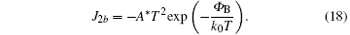
Figure 2 shows the I/V characteristic when parameter α takes different values (i.e., 2, 2.5, 3, 3.5). When α = 2, the maximum positive current and negative current are 215 nA and − 210 nA, respectively. When α = 3.5, the maximum positive current and negative current are 1085 nA and − 850 nA, respectively. With the increase of α , the conductivity of memristor increases.
 | Fig. 2. The I/V characteristics for different parameter α . |
If the frequency of the applied voltage is changed, such as f = 500 Hz, 2 kHz, 5 kHz, 10 kHz, as α increases, both of the high and low resistances of the memristor decrease, as shown in Table 1; namely, the conductivity of memristor increases.
| Table 1. High and low resistances under different frequency input voltage signals and different α (the unit of the resisitance is in Mω ). |
Comparing the first term in Eq. (21) with Eq. (8), the parameter β is given by

parameter β is determined by Φ B (the barrier height) and v (the transition probability without barrier). The barrier height Φ B does not change when the material remains the same. So the parameter β is proportional to v. Given the same number of electrons, a large value of v indicates that more electrons likely penetrate the barrier to generate the current. Therefore, a larger value v will give a larger current.
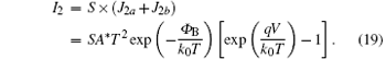
Figure 3 shows the simulation results. When β is 5, 7, 9, and 11, the corresponding maximum positive current is 113.4 nA, 187.2 nA, 236.5 nA, and 316.9 nA. Then the conductivity of memristor increases.
 | Fig. 3. The I/V characteristics for different parameter β . |
As shown in Table 2, if the frequency of the applied voltage is changed, as β increases, both of the high and low resistances of the memristor decrease; namely, the conductivity of memristor increases.
| Table 2. High and low resistances under different frequency input voltage signals and different β (the unit of the resisitance is in Mω . |
The second term of Eq. (21) represents the thermionic current when memristor is switched OFF. The parameter χ is obtained from Eq. (19)

Parameter χ is determined by both electrode’ s area S and temperature T, and is independent of the bias voltage. When the electrode’ s area S remains unchanged, the thermionic emission current through memristor changes exponentially with temperature T. Based on the thermionic emission theory, higher temperature results in the higher electrons’ kinetic energy, which allows more electrons satisfy Eq. (13). As a result, the current flowing through the memristor becomes larger.
Where the temperature is unchanged, χ is proportional to the area of electrode. Recalling the analysis of the OFF switching process above, the current density through memristor is calculated by summing up the total number of electrons penetrating the barrier in unit area per unit time. Then, the current is the product of the current density and electrode’ s area. So the number of electrons tunneling through barrier increases with the increased electrode area S, causing the current through memristor to increase.
Figure 4 shows the I– V curves when χ is 0.01, 0.1, 0.5, and 1, respectively. When χ is changed from 0.01 to 0.1, only minimal change is observed in the I– V characteristics. However, when χ is adjusted from 0.5 to 1, the current increases significantly from 458 nA to 722 nA. When χ = 1, the high resistance part approaches the low resistance part. This happens because as the temperature T goes up, the electron emission speeds up dramatically. Then, a steep increase of current through the memristor can be observed.
 | Fig. 4. The I/V characteristics of different parameter χ . |
As shown in Table 3, with applied voltage of different frequency, as χ increases, both of the high and low resistances of the memristor decrease, then the current increases, which is the same as the analysis above.
| Table 3. High and low resistances under different frequency input voltage signals and different χ (the unit of the resisitance is in MΩ ). |
The doping concentration of the memristor discussed in Section 2 is 0.5%. With the external field applied, the oxygen vacancies transfer to the Pt/TiO2− x interface, which makes the oxygen vacancies concentration at the interface of the Pt/TiO2 decrease. So it is pure TiO2. γ can be given by comparing Eqs. (21) and (19) which is mainly used to present the relationship between the current through the memristor and the external voltage V

The parameter γ is inversely related to temperature T. So this part will mainly discuss the influence of temperature T on the conductivity under the condition of low oxygen vacancy concentration. Based on the theory of the semiconductor’ s conductivity, the drift mobility is determined by the lattice scattering under the circumstance of the low oxygen vacancy concentration. As temperature T increases, the scattering probability becomes bigger, finally it makes drift mobility decrease. Owing to the reverse relationship between the resistivity and electron drift mobility, the resistivity of memristor becomes big as the drift mobility decreases. Eventually, it makes the current through memristor become small. In other words, the reduction in γ (due to the above mentioned increase in temperature T) causes the current through the memristor to decrease.
The I– V characteristics of memristor are shown in Fig. 5 when γ is set to 4, 6, 7, and 8. The change of parameter γ has a little influence on the memristor when γ = 4, 6. When γ = 7, 8, the current dramatically increases from 316 nA to 487 nA. We can observe that the high resistance part comes closely to the low resistance part when γ = 8. According to the theory of quantum tunneling, when the temperature T falls low enough, the tunneling current becomes dominant, which causes the high resistance close to the low resistance.
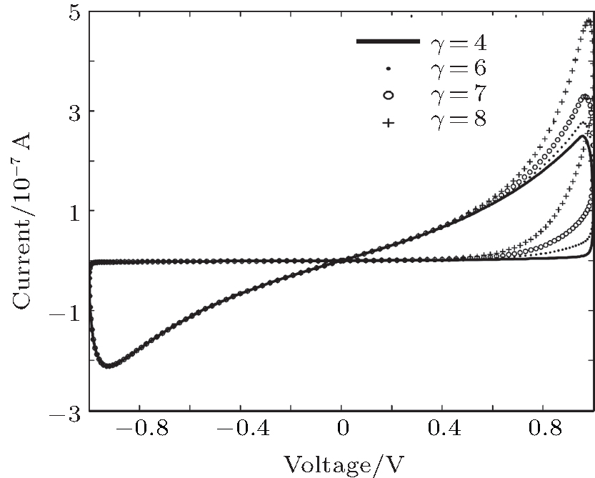 | Fig. 5. The I/V characteristics of different parameter γ . |
In Table 4, with different frequency applied voltage, as γ increases, both of the high and low resistances of the memristor decrease, and then the current increases, which is the same as the analysis above.
| Table 4. High and low resistances under different frequency input voltage signals and different γ (the unit of the resisitance is in MΩ ). |
Remark 2 As illustrated in Subsection 2.2, when a negative voltage is applied to the memristor, the thermionic emission current generated by switch-OFF process is at the leading position. When the external negative voltage is applied to the top Pt electrode, the barrier height at the semiconductor increases. The number of electrons flowing from semiconductor to metal decreases, and then the electrons flowing from metal to semiconductor play the dominant role. Because the barrier height at the metal is relatively large, it is difficult for electrons in the metal to surmount. Then the number of electrons flowing from metal to semiconductor is very small. Namely, the current from semiconductor to metal is very small. Also, the barrier at the metal remains unchanged when the external voltage changes, so the current from semiconductor to metal is constant. Therefore, the external voltage has no effect on the current when a negative voltage is applied to memristor. Because the parameters χ and γ present the voltage’ s effect on the current of memristor when the memristor is switched OFF, the changes in parameters χ and γ have no effect on the negative part of the I– V curve.
In this paper, the mechanism for the switching behavior of the memristor has been elaborated, which includes the quantum tunnel effect when the memristor is switched to the ON state, and Schottky thermionic-emission theory when the memristor is switched to the OFF state. Based on the mechanism and the exponential ionic drift equation, the relationships between each parameter in exponential model and the switching mechanism are analyzed at great length. The changes in the physical parameters of the switching process bring about the variations in the parameter α , β , χ , γ of the exponential model. When these parameters become bigger, the current through memristor increases, which is validated by the simulation results on HSPICE. It is believed that the analysis of the parameter α , β , χ , γ may be useful for the choice of the parameters’ proper values, which is meaningful for future research.
| 1 |
|
| 2 |
|
| 3 |
|
| 4 |
|
| 5 |
|
| 6 |
|
| 7 |
|
| 8 |
|
| 9 |
|
| 10 |
|
| 11 |
|
| 12 |
|
| 13 |
|
| 14 |
|
| 15 |
|
| 16 |
|
| 17 |
|
| 18 |
|
| 19 |
|
| 20 |
|
| 21 |
|
| 22 |
|
| 23 |
|
| 24 |
|
| 25 |
|
| 26 |
|
| 27 |
|
| 28 |
|
| 29 |
|
| 30 |
|
| 31 |
|
| 32 |
|
| 33 |
|