
Antiferromagnetic and topological states in silicene: A mean field study
[Liu Fenga), b) , Liu Cheng-Chengb) , Yao Yu-Gui†b)  ]
]
]
|
|


†Corresponding author. E-mail: ygyao@bit.edu.cn
*Project supported by the National Key Basic Research Program of China (Grant Nos. 2014CB920903, 2013CB921903, 2011CBA00108, and 2012CB937500), the National Natural Science Foundation of China (Grant Nos. 11021262, 11172303, 11404022, 11225418, and 11174337), the Specialized Research Fund for the Doctoral Program of Higher Education of China (Grant No. 20121101110046), the Excellent Young Scholars Research Fund of Beijing Institute of Technology (Grant No. 2014CX04028), and the Basic Research Funds of Beijing Institute of Technology (Grant No. 20141842001).
It has been widely accepted that silicene is a topological insulator, and its gap closes first and then opens again with increasing electric field, which indicates a topological phase transition from the quantum spin Hall state to the band insulator state. However, due to the relatively large atomic spacing of silicene, which reduces the bandwidth, the electron–electron interaction in this system is considerably strong and cannot be ignored. The Hubbard interaction, intrinsic spin orbital coupling (SOC), and electric field are taken into consideration in our tight-binding model, with which the phase diagram of silicene is carefully investigated on the mean field level. We have found that when the magnitudes of the two mass terms produced by the Hubbard interaction and electric potential are close to each other, the intrinsic SOC flips the sign of the mass term at either K or K′ for one spin and leads to the emergence of the spin-polarized quantum anomalous Hall state.
Silicene, a monolayer honeycomb structure of silicon atoms, considered as a cousin of graphene, has aroused much concerns and is studied both theoretically and experimentally.[1– 17] Because of the similar honeycomb lattice, silicene inherits most of marvellous properties in graphene including the linear energy– momentum dispersion relation and also the topological properties. On the other hand, the unique low-buckled geometry of silicene results in some outstanding properties, such as the observable quantum spin Hall effect (QSHE) in an experimentally accessible temperature[2] and the tunable electrical band gap under a perpendicular electric field, [5, 6] which is considered to be a major obstacle for applications of graphene in devices. What is more, since the inversion symmetry of silicene could be broken by this electric field, some novel topological states can also be induced.[7, 8, 10]
When referring to the geometrical features of “ honeycomb lattice” and “ height differences for sublattices” , silicene is not the only candidate that comes to mind, actually, bilayer graphene (BLG) does also have these features. Recently, several experiments showed clear evidences that BLG at the charge neutrality point had a gapped ground state (the magnitude of the gap is about 2 meV), [18– , 23] where the original degeneracy is considered to be lifted by the formation of certain ordered ground states. Since the nearly quadratic dispersion at low energy leads to finite density of states at the Fermi level, the system is susceptible to even weak interactions. Considering pseudospin (i.e., which layer), valley, and real electron spin degrees of freedom, various broken-symmetry phases have been predicted or considered.[24– 39] Among these phases, the antiferromagnetic (AFM) state[31, 36– 39] is considered to be the most possible one, due to its consistency with the later observations including their response to a perpendicular electric field[18, 23] and tilted magnetic field.[22] Noticing the striking similarity between BLG and silicene, the electron– electron interaction might induce magnetism for silicene, and the competition between the magnetic state and topological state may lead to new physics, which is worthwhile to be carefully studied.
In this paper, with the Hubbard interaction, intrinsic SOC and electric field in our tight-binding model, a systematic investigation on the phase diagram of silicene is provided. The paper is organized as follows: in Section 2, first-principle calculations of silicene are revisited. Then, the tight-binding model is introduced in Section 3 and the corresponding phase diagram is given in Section 4. We conclude this paper in Section 5 with a brief summary.
The electronic structure of silicene is obtained self-consistently by using the PAW (projector augmented wave) pseudopotential method implemented in the VASP package.[40] The exchange-correlation potential is treated by PBE (Perdew– Burke– Ernzerhof) potential.[41]
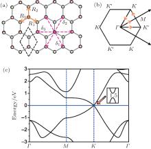
In our PBE+ SOC calculations, the k-mesh is 33 × 33 × 1, the energy cutoff and convergence criteria are set to be 400 eV and 10− 6 eV respectively. The geometry and first Brillouin zone of silicene can be found in Figs. 1(a) and 1(b). The band structure of the quantum spin Hall (QSH) state is given in Fig. 1(c), and the gap is about 1.5 meV.[2, 5]
 | Fig. 1. Geometry, Brillouin zone, and electronic structure. (a) The geometry of silicene. (b) The corresponding Brillouin zone. (c) The band structure of the QSH state, where the inset is the zooming gap with size marked, and the unit is in meV. |
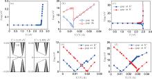
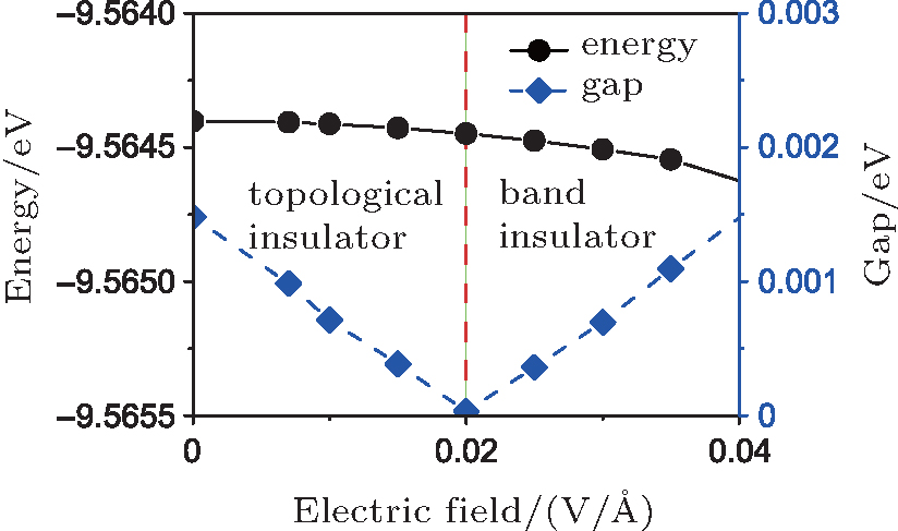 | Fig. 2. The energy and band gap with respect to the perpendicular electric field through first-principle calculations. The critical electric field 0.02 V/Å is marked with red dash line, which separates the topological insulator state from the band insulator state (topological trivial). |
The low-buckled geometry, which makes silicene different from graphene, can be well taken advantage of by applying an electric field. Therefore, we investigated the behavior of the band gap and energy with respect to the perpendicular electric field. In Fig. 2, one can see with an increasing electric field the band gap of the QSH state first closes then opens again, which is the consequence of topological phase transition, [9] and the critical electric field (about 0.02 V/Å ) is consistent with Ref. [5]. The first principle calculations help us understand the basic electrical properties of silicene based on single electron approximation. However, due to the relatively large atomic spacing of silicene, which reduces the bandwidth, the electron– electron interaction in this system is considerably strong and cannot be ignored, [42] and therefore a further investigation on the influence of electron– electron interaction to silicene is needed.
The Hubbard interaction, SOC, and electric field are taken into consideration in our tight-binding model, and the total Hamiltonian is given as H = H0 + HU + HV. The first term H0 is the low-energy effective Hamiltonian involving the SOC in silicene introduced in Ref. [3]:
where 

The second term HU is the Hubbard interaction, to be exact,

and U represents the Hubbard interaction strength. The fluctuation term U∑ i(ni↑ − ⟨ ni↑ ⟩ )(ni↓ − ⟨ ni↓ ⟩ ) is omitted under the mean field approximation. To discuss the electric field effect in silicene, we add the third term, i.e., the staggered potential term

where l = 1, 0 correspond to A and B sublattices respectively. The total Hamiltonian can be transformed into a 4 × 4 matrix H(k) for each crystal momentum k on the basis of {ψ A↑ , ψ B↑ , ψ A↓ , ψ B↓ }

and H0(k), HU(k), and HV(k) are given as follows:

 | (6) |

where f(k) = ∑ α eik· Rα , with Rα (α = 1, 2, 3) to be the nearest-neighbor vector, and 
In the case without SOC, using the Hamiltonian at the mean-field level given by Eqs. (4)– (7), we can solve this problem self-consistently. Note that there are two atoms in a unit cell, as shown in Fig. 1(a), and thus four mean fields are needed in our model considering spin degree of freedom. With λ SO = 0 and V = 0, the critical value Uc = 2.485 eV is obtained in our calculation (see Fig. 3(a)), and (Uc/t) ≈ 2.2 is consistent with previous works.[43, 44] With λ SO = 0, V ≠ 0, and fixed U = 2.492 eV slightly larger than Uc, the variations of the gaps for different spins with respect to V are plotted in Fig. 3(b), where a first order phase transition (from the AFM state to the charge density wave (CDW) state, since the corresponding on site spin polarization ni↑ − ni↓ vanishes during this process and the charge polarization na − nb ≠ 0) can be seen.
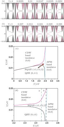
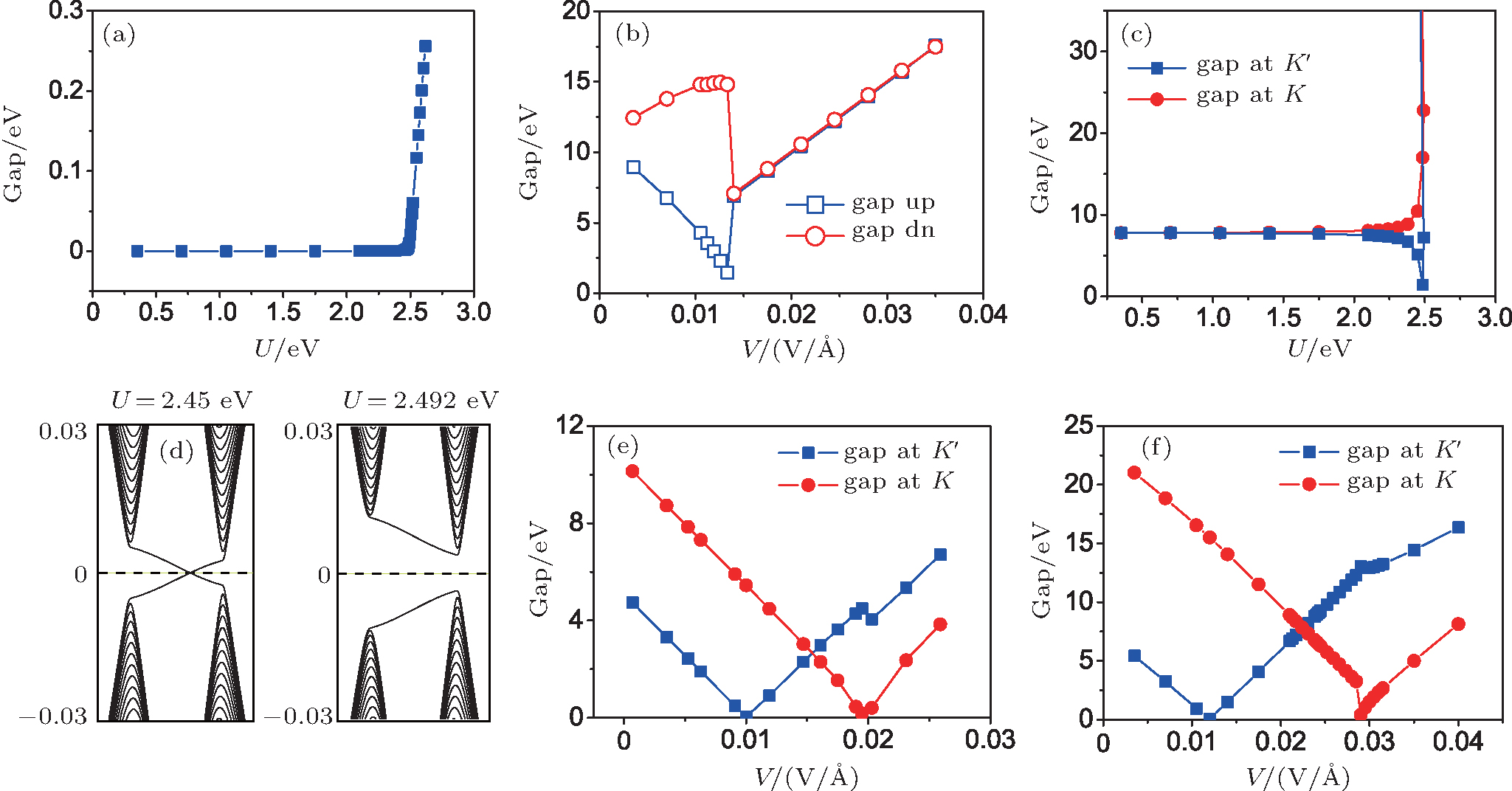 | Fig. 3. The results of mean-field self-consistent calculations. (a) Without the intrinsic SOC and electric field, the band gaps at K and K′ as functions of the Hubbard U. (b) Without the intrinsic SOC, the band gaps for different spins as functions of the electric potential for U = 2.492 eV. (c) With the intrinsic SOC and zero electric field, the band gaps at K and K′ as functions of the Hubbard U, and the edge states for U = 2.45 eV and U = 2.492 eV in panel (d). With the intrinsic SOC, the band gaps at K and K′ with respect to the electric potential are given in panels (e) and (f) for U = 2.45 eV and U = 2.492 eV respectively. |
In the case with SOC, the QSHE has been proposed in silicene, [2] by exploiting adiabatic continuity and the direct calculation of the Z2 topological invariant. The band gap opened by the SOC is about 1.5 meV, leading to the observable QSHE in an experimentally accessible temperature. However, considering the weakness of the SOC in silicene, it would be interesting to find if there are any new phases obtained from the competition between the SOC and Hubbard interaction. Therefore their phase diagram should be systematically studied.
Here we will use the tight-binding model introduced above, with the intrinsic SOC (λ SO = 3.9 meV) turned on, to discuss this issue. The behavior of the gap with respect to U (see Fig. 3(c)) is nearly the same as the one without the intrinsic SOC discussed above (see Fig. 3(a)). However, the sizes of the band gaps at K and K′ become different now. For the former, with the increasing Hubbard U the gap grows slowly until the critical value about 2.485 eV, after which there will be a rapid increase. Whereas the latter changes in a different way, first the gap becomes small, but once the Hubbard U exceeds the threshold value approximately 2.485 eV, the gap turns to increase.
One is naturally invited to the question: what happened in this process, especially, whether the gap at K′ closed at the vicinity of U = 2.485 eV, since the numerical calculation is not easy to capture this detail considering the sensitivity for parameters near the phase transition. To answer this question, we study the edge states of the zigzag edged nanoribbon of silicene. The edge states for U = 2.45 eV and U = 2.492 eV are given in Fig. 3(d), and it is obvious that there is a topological phase transition underlying this process. Therefore, the behavior of band gap is not hard to understand: when U = 0 eV, with the intrinsic SOC silicene is in the QSH state, [2, 3] and the sign of the mass term flips at either K or K′ . However, keep increasing the Hubbard U, which provides a k-spatial uniform mass term from the point view of the mean-field approximation, will finally drive the system into the topological trivial state, and at the topological phase transition point the band gap of silicene must close. We also calculate Chern number and spin-Chern number as an argument, the definition of which are C = C↑ + C↓ and Cs = (C↑ − C↓ )/2 respectively. The results are just as we expect, for U = 2.45 eV (C, Cs) = (0, − 1) and for U = 2.492 eV (C, Cs) = (0, 0).
We now proceed to discuss the effect of electric field to silicene. Two typical values of Hubbard U = 2.45 eV and U = 2.492 eV are chosen to study the variation of the system with respect to the electric potential V, and the entire phase diagram will be left for the next section.
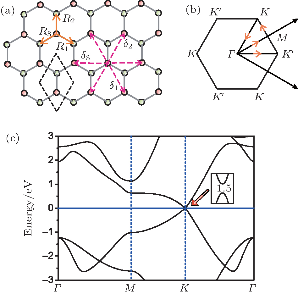
With respect to the electric potential, the band gaps at K and K′ are given in Figs. 3(e) and 3(f) for U = 2.45 eV and U = 2.492 eV respectively, from which we can see the gaps at K and K′ both first become small, and when the electric field exceeding certain values, they start to increase. To comprehend these two processes, we investigated the evolution of the edge states with respect to the electric field shown in Figs. 4(a) and 4(b). Note that due to the first order phase transition in Fig. 4(b), we fail to capture the moment of the closure of the gap at K for U = 2.492 eV, but with the analysis of the edge states and also the following calculation of Chern number, this closure can be confirmed. With U = 2.45 eV, (C, Cs) = (0, 1) (QSH) for V = 0, 0.0035 eV, (C, Cs) = (1, 1/2) for V = 0.0147 eV, (C, Cs) = (0, 0) (trivial) for V = 0.0231 eV, and the system is at the phase transition critical point when V = 0.01, 0.0195 eV. It is worth noting that (C, Cs) = (1, 1/2) represents the system is spin-polarized, and this state is therefore named spin-polarized quantum anomalous Hall (SQAH) state.[10] For U = 2.492 eV, the (C, Cs) is (0, 0) for V = 0.0, 0.007, 0.029, 0.035 eV, (1, − 1/2) for V = 0.021 eV, V = 0.012 eV is the phase transition critical point, and the phase transition critical point near V = 0.029 is not captured due to the first-order phase transition mentioned above. These two parameter paths are marked in Fig. 4(d).
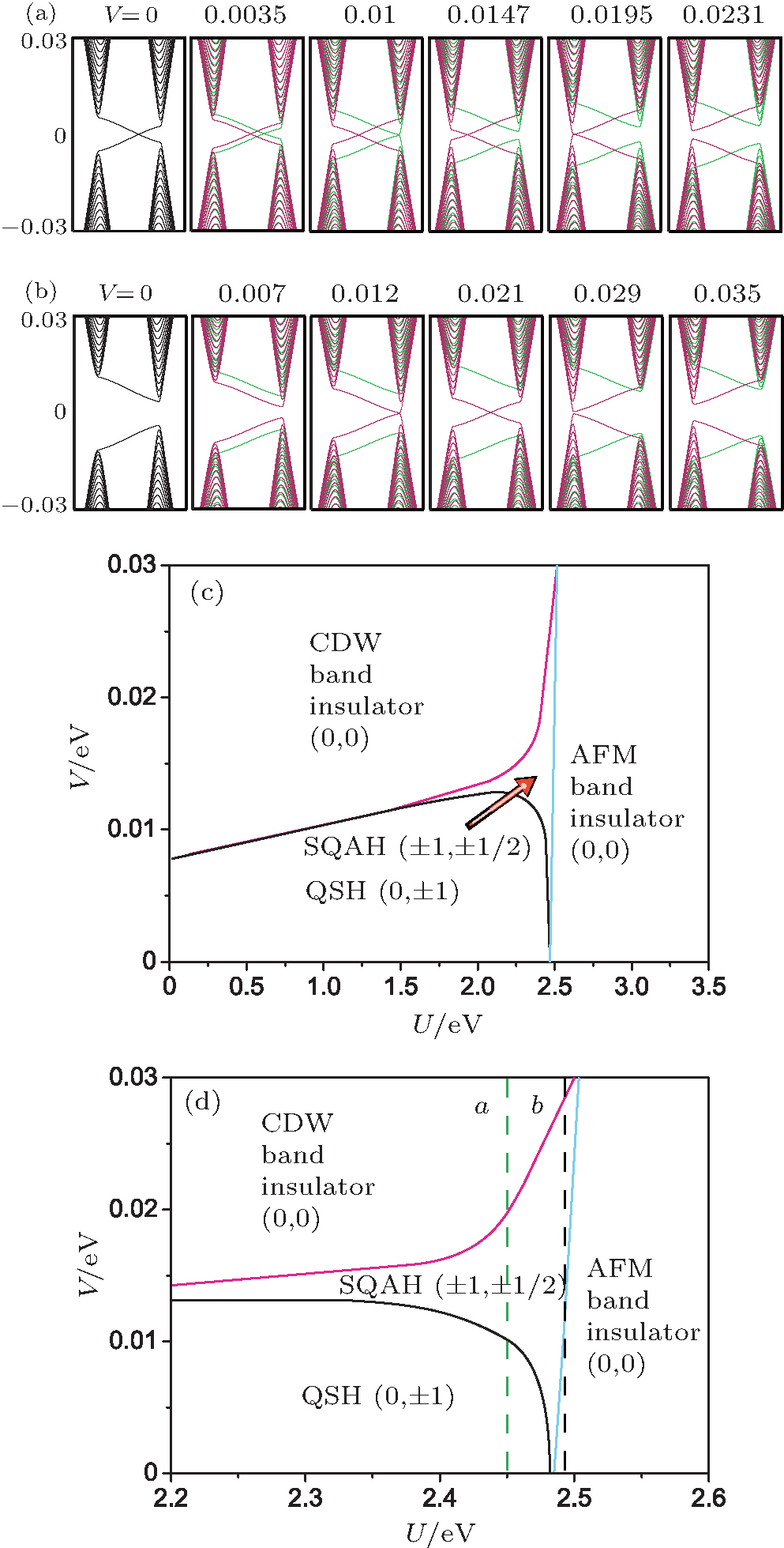 | Fig. 4. (a) The edge states for U = 2.45 eV, with V = 0.0, 0.0035, 0.01, 0.0147, 0.0195, 0.0231 eV. (b) The edge states for U = 2.492 eV, with V = 0.0, 0.007, 0.012, 0.021, 0.029, 0.035 eV. Different colors represent different spins. (c) The schematic phase diagram. There are four phases as indicated by QSH state, CDW band insulator, AFM band insulator, and SQAH state. The corresponding (C, Cs) of four phases are given to help understanding. The paths of panels a and b are marked in the zooming phase diagram (d). |
The physics in the above process can be understood from the competition between two different mass terms produced by the Hubbard U and electric potential V. However, due to the k-spatial uniform property of these two mass terms, the non-trivial topological state cannot be induced by themselves, and only when the magnitudes of these two mass terms are close to each other, can the intrinsic SOC flip the sign of the mass term at either K or K′ for one spin and lead to the emergence of the topological state, i.e., the SQAH state.
After acquainting with the phase transition at a fixed Hubbard U as a function of the electric potential V, we next investigate the phase diagram for the whole (U, V) plane. Actually, all of these phases, which can be obtained in this plane, have been discussed above, and we can determine phase boundaries by scanning the points with zero band gap at K or K′ .
In Fig. 4(c), there are four phases, named QSH state, CDW band insulator, AFM band insulator, and SQAH state. The results can be understood as the following aspects. When both U and V are small, the intrinsic SOC dominates, and because the gap keeps open during this adiabatic process, it must be in the same topological state as the original one, viz QSH state. To increase no matter U or V will finally drive this system turning into a trivial insulator state, for the former it will be the AFM band insulator (two sublattices have opposite spin polarization directions), while, for the later it will be the CDW band insulator (different charge densities for two sublattices). The intrinsic SOC will help to induce the SQAH state in the region where the magnitudes of the two mass terms produced by U and V are close to each other.
To summarize, the topological properties of silicene are revisited and confirmed with first principles calculations. To consider the influence of electron– electron interaction on silicene, the intrinsic SOC, Hubbard interaction, and electric field are taken into consideration in our tight-binding model on the mean-field level. Then, with this tight-binding model, the phase diagram of silicene is revealed, and we find that the appearance of the spin-polarized quantum anomalous Hall (SQAH) state stems from the competition between the electric field and Hubbard interaction.
| 1 |
|
| 2 |
|
| 3 |
|
| 4 |
|
| 5 |
|
| 6 |
|
| 7 |
|
| 8 |
|
| 9 |
|
| 10 |
|
| 11 |
|
| 12 |
|
| 13 |
|
| 14 |
|
| 15 |
|
| 16 |
|
| 17 |
|
| 18 |
|
| 19 |
|
| 20 |
|
| 21 |
|
| 22 |
|
| 23 |
|
| 24 |
|
| 25 |
|
| 26 |
|
| 27 |
|
| 28 |
|
| 29 |
|
| 30 |
|
| 31 |
|
| 32 |
|
| 33 |
|
| 34 |
|
| 35 |
|
| 36 |
|
| 37 |
|
| 38 |
|
| 39 |
|
| 40 |
|
| 41 |
|
| 42 |
|
| 43 |
|
| 44 |
|