Comparison of electronic structure between monolayer silicenes on Ag (111)\
Chun-Liang Lin†a)  , Ryuichi Arafune
b) , Maki Kawaia) , Noriaki Takagi‡a)
, Ryuichi Arafune 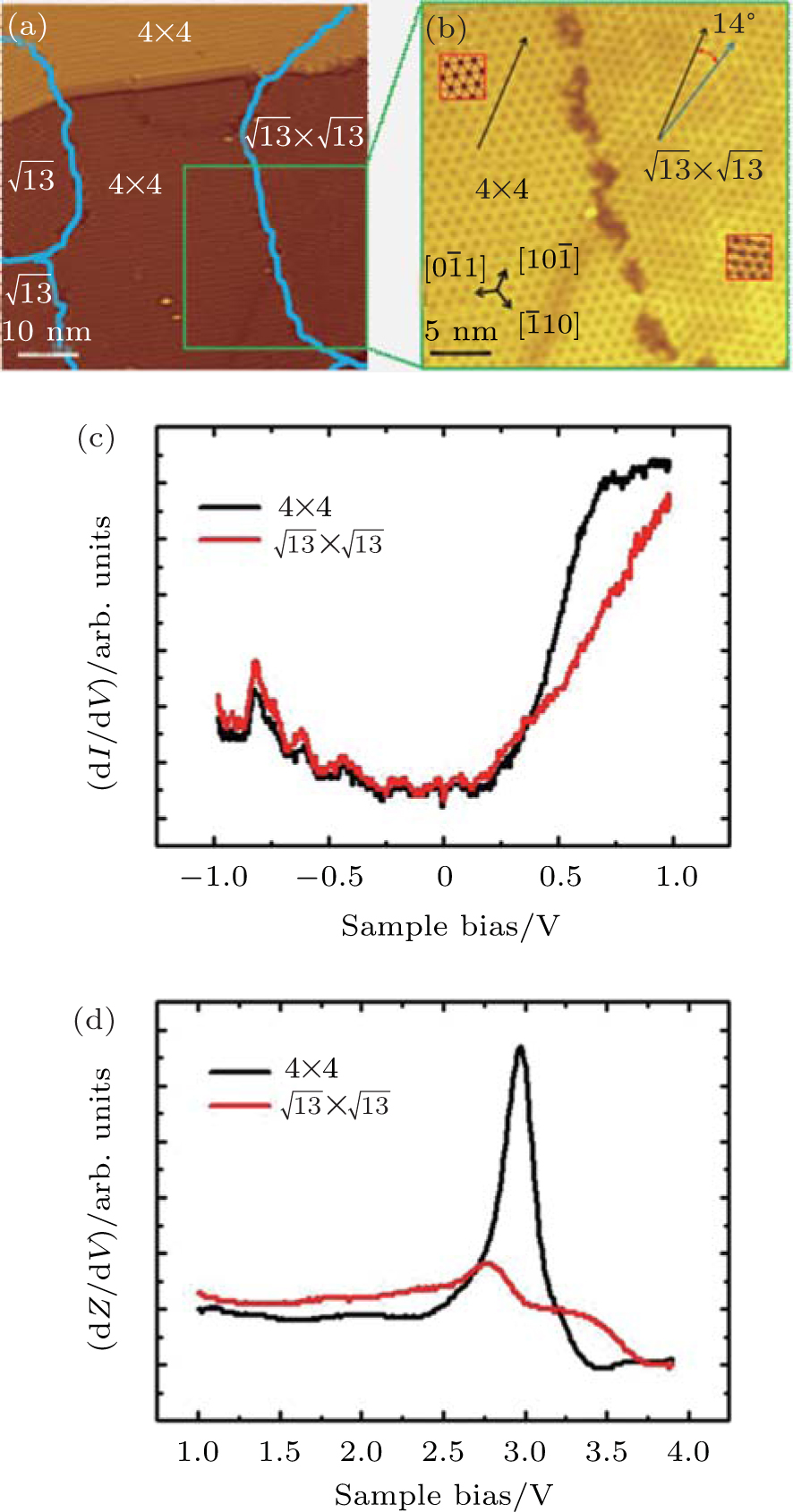
Comparison of electronic structure between monolayer silicenes on Ag (111)\ |
|
Chun-Liang Lin†
, Ryuichi Arafune |
| (a) Topographic STM image of monolayer silicene on Ag (111) at a sample bias of V s = 0.5 V and tunneling current of I t = 0.2 nA. The image size is 60 nm × 60 nm. Both 4 × 4 and phases coexist on the surface. The blue curves indicate the domain boundaries. (b) The zoom-in image of the green square in panel (a) with V s = 0.5 V, I t = 0.2 nA, and size is 30 nm × 30 nm. The 4 × 4 phase matches the symmetry axes of the Ag (111) substrate while the phase rotates an angle of 14°. High resolution images (3.5 nm × 3.5 nm, V s = −0.02 V, and I t = 0.2 nA) of defined areas are attached in the image. (c) d I /d V spectra and (d) d Z /d V spectra of the 4 × 4 and phases taken by a lock-in technique. The modulation voltages of panel (c) 4 mV at 512 Hz and panel (d) 14 mV at 512 Hz are added to the sample voltage in the lock-in measurements. |
| |