Comparison of electronic structure between monolayer silicenes on Ag (111)
Chun-Liang Lin†a), Ryuichi Arafuneb), Maki Kawaia), Noriaki Takagi‡a)
Department of Advanced Materials Science, Graduate School of Frontier Science, The University of Tokyo, 5-1-5 Kashiwa, Chiba 277-8561, Japan
International Center for Materials Nanoarchitectonics (WPI-MANA), National Institute for Materials Science, 1-1 Namiki, Ibaraki 304-0044, Japan

Corresponding author. E-mail: clin@ams.k.u-tokyo.ac.jp

Corresponding author. E-mail: n-takagi@k.u-tokyo.ac.jp

*Project supported by the Ministry of Education, Culture, Sports, Science and Technology (MEXT) through Grants-in-Aid for Scientific Research (Grant Nos. 24241040 and 25110008) and the World Premier International Research Center Initiative (WPI), MEXT, Japan.

Abstract

The electronic structures of monolayer silicenes (4 × 4 and) grown on Ag (111) surface are studied by scanning tunneling spectroscopy (STS) and density functional theory (DFT) calculations. While both phases have similar electronic structures around the Fermi level, significant differences are observed in the higher energy unoccupied states. The DFT calculations show that the contributions of Si 3p z orbitals to the unoccupied states are different because of their different buckled configurations.

PACS: 73.22.–f; 68.37.Ef; 61.46.–w; 81.05.Zx
Keyword: silicene; electronic structure; STM; DFT
1. Introduction

Silicene, the two-dimensional (2D) honeycomb lattice of Si atoms, has received a lot of attention because it shares remarkable properties with graphene. Density functional theory (DFT) calculations[1, 2] have demonstrated that freestanding silicene takes a buckled structure where two Si atoms in the unit cell are displaced in the opposite directions perpendicular to the basal plane. In spite of the buckling, silicene hosts Dirac fermions similarly to graphene. The combination of the Dirac fermion characteristics with sizable spin-orbital coupling (SOC) of Si adds exotic properties to silicene.[36] An energy gap opens at the Dirac cone where two linear bands cross at the Fermi level, and topologically protected states emerge at the edges of 2D silicene. This indicates that silicene is promising as a material for realizing the theoretical prediction of Kane and Mele.[7] Besides, silicene is expected to be compatible with the current process technologies to fabricate electronic devices on Si platform.

In the last few years, silicene has not been only in the theoretical calculation; it has successfully been synthesized on many different substrates, such as Ag  (110), [8] Ag  (111), [911] Ir  (111), [12] ZrB2-covered Si  (111), [13] and MoS2 crystal, [14] of which, the silicene synthesized on Ag  (111) is investigated most.[911, 1539] Several phases such as 4 × 4, , etc.  are observed by using low-energy electron diffraction (LEED) and scanning tunneling microscopy (STM). For some of them, the structural models consisting of buckled honeycomb lattice have been proposed.[911, 1521] Although it has been proved that Dirac fermions disappear in the monolayer silicene on the Ag  (111) surface due to the strong hybridization with the Ag  (111) substrate, [2528, 3639] theoretical calculations predicted that the Dirac fermion characteristics can be preserved in some structures of silicene after they have been extracted from the Ag  (111) substrate.[27, 33, 34] Recently, a field effect transistor (FET) has been fabricated by transferring silicene from Ag  (111) to an Al2O3/SiO2 substrate.[40] Since various different monolayer phases appear on Ag  (111) surface, it is of great importance to reveal the electronic structures of silicenes in different configurations if they are used in the devices. In this paper, we compare the electronic structures of two dominant phases, 4 × 4 and , based on the results acquired by both scanning tunneling spectroscopy (STS) and DFT calculations.

2. Experiment

The whole experiments were performed in an ultra-high vacuum chamber with a base pressure less than 1 × 10− 10  Torr (1  Torr = 1.33322 × 10²  Pa). To grow silicene on Ag  (111) substrate, Si atoms were deposited onto the clean Ag  (111) substrate in a constant rate of 0.03  ML/min (1  ML = 1 × 10¹⁵  atoms· cm− 2 from a heated (> 1100  ° C) Si wafer. The Ag  (111) substrate was cleaned by repeated cycles of Ar + sputtering and annealing at 500  ° C. The trick to crystalize silicene is the precise control of the Ag  (111) substrate temperature. In our experiments, the temperature was kept at 260  ° C during the deposition. After sample preparation, the STM and STS measurements were carried out at 6  K.

The DFT calculations were carried out by the plane-wave-based Vienna Ab initio Simulation Package (short as VASP)[41, 42] with the projected augmented wave (PAW)[43] potentials in the generalized gradient approximation (GGA). The exchange– correlation functional of Perdew– Burke– Ernzerhof (PBE)[44] was used. The kinetic-energy cutoff for the plane-wave basis was set to be 400  eV. The silicene grown on Ag  (111) was modeled by using a supercell, which consists of a silicene layer on a 5-layer Ag slab with a vacuum of ∼ 18  Å thick along the surface normal. The supercell used for the 4 × 4 () phase was composed of 80  Ag and 18  Si (65  Ag and 18  Si) atoms. The atoms in the bottom two layers were fixed at their ideal bulk positions during the structure optimization. The positions of atoms in silicene and top three layers of the Ag slab were optimized without any constraint until the forces on individual atoms were less than 0.01  eV/Å . In the self-consistent total energy calculations, the Brillouin zone was sampled with (5 × 5 × 1) k-points.

3. Results and discussion

Figure  1(a) shows an STM image of monolayer silicene grown on Ag  (111). Both 4 × 4 and phases coexist on the surface. A zoom-in image of the green square in Fig.  1(a) is shown in Fig.  1(b). Taking a careful look at the high-resolution image on the left side of the image, one can see six protrusions and a darker hole in the unit cell. This feature indicates that the left side is attributed to the 4 × 4 phase. On the right side separated by a domain boundary, phase appears. The angle difference between two phases is ∼ 14° as indicated by the black and blue arrows.

Figure  1(c) shows the typical STS spectra acquired on 4 × 4 and phases. The spectra are obtained by a lock-in technique with a modulation voltage of 4  mV at 512  Hz added to the sample voltage. The spectra do not show strong dependence on the position inside the unit cell. The spectrum of 4 × 4 phase is similar to that of phase. Two spectra almost overlap each other in the range from − 1.0  V to 0.5  V. A difference is observed in the range from 0.5  V to 1.0  V; the intensity of 4 × 4 phase is stronger than that of phase. We consider that this difference is minor and the electronic structures of 4 × 4 and phases are essentially analogous around the Fermi level.

In contrast, the unoccupied electronic states in higher energy range are different. Figure  1(d) shows the dZ/dV spectra acquired in a bias range from 1.0  V to 3.8  V. In the

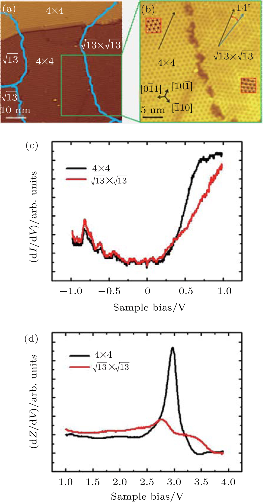
Fig.  1. (a) Topographic STM image of monolayer silicene on Ag  (111) at a sample bias of Vs = 0.5  V and tunneling current of It = 0.2  nA. The image size is 60  nm × 60  nm. Both 4 × 4 and phases coexist on the surface. The blue curves indicate the domain boundaries. (b) The zoom-in image of the green square in panel (a) with Vs = 0.5  V, It = 0.2  nA, and size is 30  nm × 30  nm. The 4 × 4 phase matches the symmetry axes of the Ag  (111) substrate while the phase rotates an angle of 14° . High resolution images (3.5  nm × 3.5  nm, Vs = − 0.02  V, and It = 0.2  nA) of defined areas are attached in the image. (c) dI/dV spectra and (d) dZ/dV spectra of the 4 × 4 and phases taken by a lock-in technique. The modulation voltages of panel  (c) 4  mV at 512  Hz and panel  (d) 14  mV at 512  Hz are added to the sample voltage in the lock-in measurements.

ZV spectrum, the displacement of the tip (Z) is measured as a function of bias voltage (V) applied to the STM junction with holding the feedback loop on. The tip promptly retracts from the surface to keep the tunneling current constant when the density of states increases at certain voltages. In other words, the displacement of the tip depends on how the density of states varies with energy. By differentiating the ZV curve, peaks appear at the voltages where the density of states is relatively high. Therefore, the dZ/dV spectrum is basically proportional to the density of states; it reveals the electronic structure as well as the conventional STS spectrum.[4547] The spectra shown here are obtained by a lock-in technique with a modulation voltage of 14  mV at 512  Hz. A sharp peak appears at 2.95  V in 4 × 4 phase while a broad peak around 2.70  V and a shoulder near 3.40  V are observed for phase. These spectral signatures show the difference in electronic structures between the two phases.

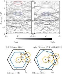
To understand the variations in the electronic structures of two phases, the electronic band structures are calculated for both 4 × 4 and phases. The calculated band structures of 4 × 4 and phases are shown in Figs.  2(a) and 2(b), respectively. The contribution of Si 3pz orbital is indicated by the gradient bar. The higher contribution appears in darker colors. The Brillouin zone (BZ) of each structure is shown in Figs.  2(c) and 2(d). Note that the K point (K1) in the BZ of silicene 1 × 1 overlaps with the Γ point (Γ 2) in the extended BZs of 4 × 4 or phases. Thus the band structures in Figs.  2(a) and 2(b) are drawn along the high symmetry directions in the BZs. Both band structures become complicated because of the following reasons. (i) The bulk bands are discretized because we describe the system as a slab model. Although the bulk Ag bands essentially should appear as a background, they appear as many branches to

Fig.  2. Calculated band structures of (a) 4 × 4 and (b) . The gradient bar manifests the contribution of Si 3pz orbital to each branch. The darker the region, the higher the contribution in the region is. Panels  (c) and (d) indicate the Brillouin zones (BZs) of 4 × 4 and phases together with the BZs of Ag  (111) 1 × 1 and silicene 1 × 1. The yellow hexagons in panels  (c) and (d) represent the BZs of 4 × 4 and phases, respectively. The blue hexagons refer to the BZs of corresponding 1 × 1 honeycomb lattice in each structure. The black hexagons denote the BZs of the Ag  (111) surface. Γ 1, K1, and M1 are the highly symmetric points in the BZ of silicene 1 × 1 and Γ 2, K2, and M2 are the highly symmetric points in the BZ of 4 × 4 or .

overlap with the bands derived from Si. (ii) The bands relevant to the Si 3pz orbital hybridize with the substrate Ag states and their contributions are scattered.

The band structures of the 4 × 4 and phases are essentially similar especially near the Fermi level. The Dirac cone feature observed for the freestanding silicene disappears for both phases. The Ag  (111) surface has a band gap extending between − 0.4  eV and 3.9  eV from the lower to the upper sp-band.[4850] Although the band gap opens at the Fermi level, the lower sp-band is distributed near the Fermi level so that it strongly hybridizes with the Si 3pz orbital. The hybridization strikingly reduces the contribution of Si 3pz orbital near the Fermi level. Although the Dirac cone feature observed for the freestanding silicene should appear at the Γ 2 point for both phases, it cannot be found in Fig.  2(a) nor in Fig.  2(b). Near the Γ 2 point, the bands derived from Si 3pz orbital contribute at 1  eV above the Fermi level in both 4 × 4 and phases as marked by the blue circles in Figs.  2(a) and 2(b). These features are matched with the increase of spectral intensity near 1  eV above the Fermi level in the STS spectra as shown in Fig.  1(c).

One can easily see the difference in band structure between the 4 × 4 and phases. The contributions of Si 3pz orbital almost disappear for the energy above 1  eV in the phase but several bands generated by Si 3pz orbital appear near 3  eV above the Fermi level in the 4 × 4 phase as marked by the red circle in Fig.  2(a). This difference between the band structures can help us explain the huge diversity found in the dZ/dV spectra. A peak near 3  eV above the Fermi level is found on the 4 × 4 phase as shown in Fig.  1(d). In contrast, the spectrum of the phase is relatively broad because most of the bands near 3  eV come from the Ag substrate. The striking difference in electronic structure, originating from the different buckled configurations, is observed in the higher energy regions. This is also solid evidence to show that the different structures of silicene grown on Ag  (111) are not moiré patterns, in contrast to other honeycomb lattices on metal substrates such as graphene on Ir  (111), [51] Pt  (111), [52] Ru  (0001), [53] Cu  (111), [54] and h-BN on Cu  (111)[55]. The moiré patterns can be observed due to the mismatch between the overlayers and the substrate lattices. For example, two kinds of moiré patterns with different periodicities are observed for graphene on Cu  (111) surface while rotating the graphene lattice 7° with respect to the Cu  (111) lattice.[54] In the case of silicene on Ag  (111), it is more than the rotations of a honeycomb lattice; in fact different phases reveal different buckled configurations. The electronic structures of silicene seriously correlate with their own geometric configurations.

The difference in geometric configuration between 4 × 4 and phases is briefly described below based on our structural models. Figures  3(a) and 3(b) show calculated STM images together with the STM observations of 4 × 4 and phases, respectively. The yellow rhombuses in the middle indicate the unit cell of each phase. The simulated images reasonably agree with the real STM images, and thus the models of these two structures shown below should be very close to the real structures. The models of the 4 × 4 and phases are shown in Figs.  3(c) and 3(d), respectively. Although both 4 × 4 and phases consist of the same number of Si atoms (18 Si atoms in each unit cell), the cell size and the buckled configuration are so different: the cell sizes of the 4 × 4 and phases are 11.56  Å and 10.42  Å , respectively. From the side view of each structural model shown in Figs.  3(e) and 3(f), it is obvious that the buckled configurations in two phases are different. The phase takes a typical buckled configuration where the number of upper Si atoms in the unit cell is equal to that of lower Si atoms, while the 4 × 4 phase is another scenario. The structural parameters of these two models are listed in Table  1. It is not difficult to find that Si slightly adjusts its bond length under different conditions. For example, the bond lengths of Si– Si in 4 × 4 phase range from 2.29  Å to 2.31  Å which have been

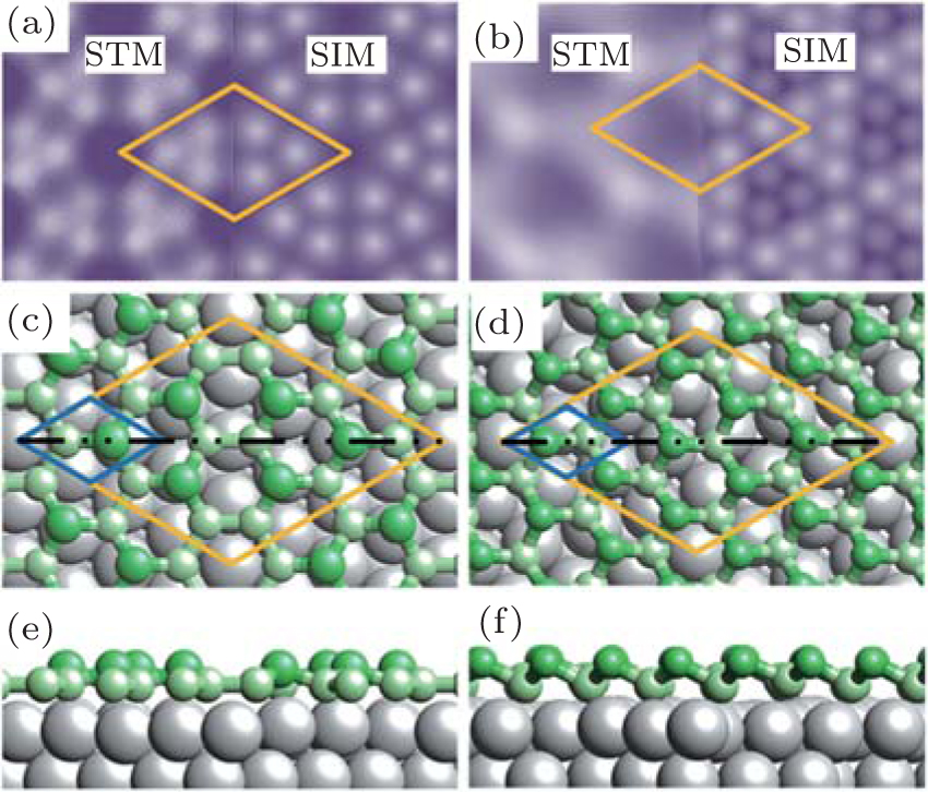
Fig.  3. (a) and (b) Simulated STM images (SIM) combined with the real STM images of the 4 × 4 and phases, respectively. Structural models of (c) 4 × 4 and (d) phases optimized by the DFT calculations. The unit cell of each model is indicated by yellow rhombus and the small blue rhombuses indicate the corresponding 1 × 1 unit cells. (e) and (f) the side views of each model.
Table 1. Structural parameters of the 4 × 4 and phases: sizes of unit cell, the variation of Si– Si bond lengths, the height difference between the highest and lowest Si atoms, and the variation of buckling angles.
determined by the tensor LEED analysis.[30] They are different from the value of 2.29  Å in phase. Therefore, different phases of silicene on Ag  (111) are caused not only by the rotation of silicene lattice but also by the modification in the Si– Si bonds. The electronic structures therefore drastically change between the two structures.

Before closing discussion, we come to discuss the geometric structure of . Up to now, at least five models have been proposed by different calculations. We have proposed a typical buckled model as shown in Fig.  3(d). Jamgotchian et al.[15] and Enriquez et al.[16] have proposed two similar models. Other two models have been recently proposed by Pflugradt et al.[33] A very recent STM observation done by Liu et al.[56] shows that the STM images match the model proposed by Jamgotchian et al. and Enriquez et al. Nevertheless, except for our model, the other models contain 14 Si atoms in the unit cell. These models provide an Si density of 1.077 Si atoms per Ag  (111) 1 × 1 unit cell, which is lower than that of the 4 × 4 phase (1.125 Si atoms per Ag  (111) 1 × 1 unit cell). In the LEED observation, the phase usually appears in higher coverage regime after the 4 × 4 phase has been formed.[19, 29] It is more convincing if the phase consists of a higher density of Si than the 4 × 4 phase. Since our model contains 18 Si atoms in the unit cell of the phase, the Si density is 1.385  Si atoms per Ag  (111) unit cell. This value is higher than that of the 4 × 4 phase and agrees with most of LEED observations. Besides, the electronic structure calculated from our model is nearly consistent with our STS and dZ/dV observations while the electronic structures[33, 35] calculated for the other models[15, 16, 35] hardly explain the current STS and dZ/dV results.

4. Conclusions

Silicene has been acknowledged as a new allotrope of Si. Comparing with graphene, silicene is more flexible in structure. Different buckled configurations are found from the silicene synthesized on Ag  (111) surface. By the combination of STS measurements and DFT calculations, we successfully find the difference in electronic structure between the 4 × 4 and phases, which arises from the different buckling configurations. In the STS measurement, similar spectra found near the Fermi level are regarded as a consequence of the hybridization with Ag  (111). The metal substrate affects the electronic structure near the Fermi level. However, a sharp peak appears at 2.95  V, far from the Fermi level, in the 4 × 4 phase whereas it is not observed in the phase. This difference originates from the different buckled configurations in the honeycomb lattice. This is verified with the DFT calculations; much stronger contribution of Si 3pz orbital is found in the 4 × 4 phase than in the phase above 3  eV from the Fermi level.

Acknowledgement

Computation in this work was performed by using the facilities of the Supercomputer Center, the Institute for Solid State Physics, University of Tokyo.

Reference
1 Takeda K and Shiraishi K 1994 Phys. Rev. B 50 14916 DOI:10.1103/PhysRevB.50.14916 [Cited within:1]
2 Cahangirov S, Topsakal M, Aktrük E, Sahin H and Ciraci S 2009 Phys. Rev. Lett. 102 236804 DOI:10.1103/PhysRevLett.102.236804 [Cited within:1]
3 Liu C C, Feng W and Yao Y 2011 Phys. Rev. Lett. 107 076802 DOI:10.1103/PhysRevLett.107.076802 [Cited within:1]
4 Ezawa M 2012 J. Phys. Soc. Jpn. 81 064705 DOI:10.1143/JPSJ.81.064705 [Cited within:1]
5 Ezawa M 2012 Phys. Rev. Lett. 109 055502 DOI:10.1103/PhysRevLett.109.055502 [Cited within:1]
6 Drummond N D, Zólyomi V and Fal’ko V I 2012 Phys. Rev. B 85 075423 DOI:10.1103/PhysRevB.85.075423 [Cited within:1]
7 Kane C L and Mele E J 2005 Phys. Rev. Lett. 95 226801 DOI:10.1103/PhysRevLett.95.226801 [Cited within:1]
8 De Padova P, Quaresima C, Ottaviani C, Sheverdyaeva P M, Moras P, Carbone C, Olivieri D T B, Kara A, Oughaddou H, Aufray B and Le Lay G 2010 Appl. Phys. Lett. 96 261905 DOI:10.1063/1.3459143 [Cited within:1]
9 Lalmi B, Oughaddou H, Enriquez H, Kara A, Vizzini S, Ealet B and Aufray B 2010 Appl. Phys. Lett. 97 223109 DOI:10.1063/1.3524215 [Cited within:3]
10 Lin C L, Arafune R, Kawahara K, Tsukahara N, Minamitani E, Kim Y, Takagi N and Kawai M 2012 Appl. Phys. Express 5 045802 DOI:10.1143/APEX.5.045802 [Cited within:1]
11 Vogt P, De Padova P, Quaresima C, Avila J, Frantzeskakis E, Asensio M C, Resta A, Ealet B and Le Lay G 2012 Phys. Rev. Lett. 108 155501 DOI:10.1103/PhysRevLett.108.155501 [Cited within:3]
12 Meng L, Wang Y, Zhang L, Du S, Wu R, Li L, Zhang Y, Li G, Zhou H, Hofer W A and Gao H 2013 Nano Lett. 13 685 DOI:10.1021/nl304347w [Cited within:1]
13 Fleurence A, Friedlein R, Ozaki T, Kawai H, Wang Y and Yamada-Takamura Y 2012 Phys. Rev. Lett. 108 245501 DOI:10.1103/PhysRevLett.108.245501 [Cited within:1]
14 Chiappe D, Scalise E, Cinquanta E, Grazianetti C, van den Broek B, Fanciulli M, Houssa M and Molle A 2014 Adv. Mater. 26 2096 DOI:10.1002/adma.201304783 [Cited within:1]
15 Jamgotchian H, Colignon Y, Hamzaoui N, Ealet B, Hoarau J Y, Aufray B and Bibérian J P 2012 J. Phys. : Condens. Matter 24 172001 DOI:10.1088/0953-8984/24/17/172001 [Cited within:4]
16 Enriquez H, Vizzini S, Kara A, Lalmi B and Oughaddou H 2012 J. Phys. : Condens. Matter 24 314211 DOI:10.1088/0953-8984/24/31/314211 [Cited within:2]
17 Feng B, Ding Z, Meng S, Yao Y, He X, Cheng P, Chen L and Wu K 2012 Nano Lett. 12 3507 DOI:10.1021/nl301047g [Cited within:1]
18 Chen L, Liu C C, Feng B, He X, Cheng P, Ding Z, Meng S, Yao Y and Wu K 2012 Phys. Rev. Lett. 109 056804 DOI:10.1103/PhysRevLett.109.056804 [Cited within:1]
19 Arafune R, Lin C L, Kawahara K, Tsukahara N, Minamitani E, Kim Y, Takagi N and Kawai M 2013 Surf. Sci. 608 297 DOI:10.1016/j.susc.2012.10.022 [Cited within:1]
20 Cinquanta E, Scalise E, Chiappe D, Grazianetti C, van den Broek B, Houssa M, Fanciulli M and Molle A 2013 J. Phys. Chem. C 117 16719 DOI:10.1021/jp405642g [Cited within:1]
21 Fukaya Y, Mochizuki I, Maekawa M, Wada K, Hyodo T, Matsuda I and Kawasuso A 2013 Phys. Rev. B 88 205413 DOI:10.1103/PhysRevB.88.205413 [Cited within:1]
22 Chen L, Liu C C, Feng B, He X, Cheng P, Ding Z, Meng S, Yao Y and Wu K 2013 Phys. Rev. Lett. 110 229702 DOI:10.1103/PhysRevLett.110.229702 [Cited within:1]
23 De Padova P, Vogt P, Resta A, Avila J, Razado-Colambo I, Quaresima C, Ottaviani C, Olivieri B, Bruhn T, Hirahara T, Shirai T, Hasegawa S, Asensio M C and Le Lay G 2013 Appl. Phys. Lett. 102 163106 DOI:10.1063/1.4802782 [Cited within:1]
24 De Padova P, Avila J, Resta A, Razado-Colambo I, Quaresima C, Ottaviani C, Olivieri B, Bruhn T, Vogt P, Asensio M C and Le Lay G 2013 J. Phys. : Condens. Matter 25 382202 DOI:10.1088/0953-8984/25/38/382202 [Cited within:1]
25 Lin C L, Arafune R, Kawahara K, Kanno M, Tsukahara N, Minamitani E, Kim Y, Kawai M and Takagi N 2013 Phys. Rev. Lett. 110 076801 DOI:10.1103/PhysRevLett.110.076801 [Cited within:1]
26 Arafune R, Lin C L, Nagao R, Kawai M and Takagi N 2013 Phys. Rev. Lett. 110 229701 DOI:10.1103/PhysRevLett.110.229701 [Cited within:1]
27 Wang Y P and Cheng H P 2013 Phys. Rev. B 87 245430 DOI:10.1103/PhysRevB.87.245430 [Cited within:1]
28 Cahangirov S, Audiffred M, Tang P, Iacomino A, Duan W, Merino G and Rubio A 2013 Phys. Rev. B 88 035432 DOI:10.1103/PhysRevB.88.035432 [Cited within:1]
29 Moras P, Mentes T O, Sheverdyaeva P M, Locatelli A and Carbone C 2014 J. Phys. : Condens. Matter 26 185001 DOI:10.1088/0953-8984/26/18/185001 [Cited within:1]
30 Kawahara K, Shirasawa T, Arafune R, Lin C L, Takahashi T, Kawai M and Takagi N 2014 Surf. Sci. 623 25 DOI:10.1016/j.susc.2013.12.013 [Cited within:1]
31 Sone J, Yamagami T, Aoki Y, Nakatsuji K and Hirayama H 2014 New J. Phys. 16 095004 DOI:10.1088/1367-2630/16/9/095004 [Cited within:1]
32 Shirai T, Shirasawa T, Hirahara T, Fukui N, Takahashi T and Hasegawa S 2014 Phys. Rev. B 89 241403 DOI:10.1103/PhysRevB.89.241403 [Cited within:1]
33 Pflugradt P, Matthes L and Bechstedt F 2014 Phys. Rev. B 89 035403 DOI:10.1103/PhysRevB.89.035403 [Cited within:3]
34 Scalise E, Cinquanta E, Houssa M, van den Broek B, Chiappe D, Grazianetti C, Pourtois G, Ealet B, Molle A, Fanciulli M, Afanas’ev V V and Stesmans A 2014 Appl. Surf. Sci. 291 113 DOI:10.1016/j.apsusc.2013.08.113 [Cited within:1]
35 Tchalala M R, Enriquez H, Yildirim H, Kara A, Mayne A J, Dujardin G, Ali M A and Oughaddou H 2014 Appl. Surf. Sci. 303 61 DOI:10.1016/j.apsusc.2014.02.064 [Cited within:2]
36 Yuan Y, Quhe R, Zheng J, Wang Y, Ni Z, Shi J and Lu J 2014 Physica E 58 38 DOI:10.1016/j.physe.2013.11.016 [Cited within:1]
37 Mahatha S K, Moras P, Bellini V, Sheverdyaeva P M, Struzzi C, Petaccia L and Carbone C 2014 Phys. Rev. B 89 201416 DOI:10.1103/PhysRevB.89.201416 [Cited within:1]
38 Stephan R, Hanf M C and Sonnet P 2015 J. Phys. : Condens. Matter 27 015002 DOI:10.1088/0953-8984/27/1/015002 [Cited within:1]
39 Ishida H, Hamamoto Y, Morikawa Y, Minamitani E, Arafune R and Takagi N 2015 New J. Phys. 17 015013 DOI:10.1088/1367-2630/17/1/015013 [Cited within:2]
40 Tao L, Cinquanta E, Chiappe D, Grazianetti C, Fanciulli M, Dubey M, Molle A and Akinwand e D 2015 Nat. Nanotechnol. 10 227 DOI:10.1038/nnano.2014.325 [Cited within:1]
41 Kresse G and Furthmüller J 1996 Phys. Rev. B 56 11169 [Cited within:1]
42 Kresse G and Furthmüller J 1996 Comput. Mater. Sci. 6 15 DOI:10.1016/0927-0256(96)00008-0 [Cited within:1]
43 Blöchl P E 1994 Phys. Rev. B 24 17953 [Cited within:1]
44 Perdew J P, Burke K and Ernzerhof M 1996 Phys. Rev. Lett. 77 3865 DOI:10.1103/PhysRevLett.77.3865 [Cited within:1]
45 Feng M, Zhao J and Petek H 2008 Science 320 359 DOI:10.1126/science.1155866 [Cited within:1]
46 Yang M C, Lin C L, Su W B, Lin S P, Lu S M, Lin H Y, Chang C S, Hsu W K and Tsong T T 2009 Phys. Rev. Lett. 102 196102 DOI:10.1103/PhysRevLett.102.196102 [Cited within:1]
47 Lin C L, Yang M C, Su W B, Lin S P, Lu S M, Lin H Y, Chang C S, Fu T Y and Tsong T T 2010 Chin. J. Phys. 48 855 [Cited within:1]
48 Miller T, McMahon W E and Chiang T C 1996 Phys. Rev. Lett. 77 1167 DOI:10.1103/PhysRevLett.77.1167 [Cited within:1]
49 Pontius N, Sametoglu V and Petek H 2005 Phys. Rev. B 72 115105 DOI:10.1103/PhysRevB.72.115105 [Cited within:1]
50 Winkelmann A, Sametoglu V, Zhao J, Kubo A and Petek H 2007 Phys. Rev. B 76 195428 DOI:10.1103/PhysRevB.76.195428 [Cited within:1]
51 N’Diaye A T, Bleikamp S, Feibelman P J and Michely T 2006 Phys. Rev. Lett. 97 215501 DOI:10.1103/PhysRevLett.97.215501 [Cited within:1]
52 Sutter P, Sadowski J T and Sutter E 2009 Phys. Rev. B 80 245411 DOI:10.1103/PhysRevB.80.245411 [Cited within:1]
53 Vázquez de Parga A L, Calleja F, Borca B, Passeggi M C G, Hinarejos J J, Guinea F and Mirand a R 2008 Phys. Rev. Lett. 100 056807 DOI:10.1103/PhysRevLett.100.056807 [Cited within:1]
54 Gao L, Guest J R and Guisinger N P 2010 Nano Lett. 10 3512 DOI:10.1021/nl1016706 [Cited within:2]
55 Joshi S, Ecija D, Koitz R, Iannuzzi M, Seitsonen A P, Hutter J, Sachdev H, Vijayaraghavan S, Bischoff F, Seufert K, Barth J V and Auwärter W 2012 Nano Lett. 12 5821 DOI:10.1021/nl303170m [Cited within:1]
56 Liu Z L, Wang M X, Xu J P, Ge J F, Le Lay G, Vogt P, Qian D, Gao C L, Liu C and Jia J F 2014 New J. Phys. 16 075006 DOI:10.1088/1367-2630/16/7/075006 [Cited within:1]