


Growth mechanism and modification of electronic and magnetic properties of silicene
[Liu Hong-Sheng, Han Nan-Nan, Zhao Ji-Jun† ]
]
]
|
|


†Corresponding author. E-mail: zhaojj@dlut.edu.cn
*Project supported by the National Natural Science Foundation of China (Grant No. 11134005).
Silicene, a monolayer of silicon atoms arranged in a honeycomb lattice, has been undergoing rapid development in recent years due to its superior electronic properties and its compatibility with mature silicon-based semiconductor technology. The successful synthesis of silicene on several substrates provides a solid foundation for the use of silicene in future microelectronic devices. In this review, we discuss the growth mechanism of silicene on an Ag (111) surface, which is crucial for achieving high quality silicene. Several critical issues related to the electronic properties of silicene are also summarized, including the point defect effect, substrate effect, intercalation of alkali metal, and alloying with transition metals.
The boom of graphene, [1, 2] which exhibits outstanding physical and chemical properties, has given rise to the exploration of other two-dimensional (2D) materials. Silicene, which is the silicon counterpart of graphene, holds great promise for future applications in microelectronic devices due to its excellent electronic properties and easy integration into current Si-based semiconductor technology. However, unlike graphene, silicene is not absolutely planar but has a buckled height of about 0.44 Å .[3, 4] In spite of the low buckled geometry, silicene possesses outstanding electronic properties similar to those of graphene.[1– 11] Most importantly, silicene is a zero-gap semiconductor with linear dispersion around Fermi level, forming the famous “ Dirac cone” at the symmetric point K in the reciprocal space. The charge carriers in silicene behave like massless Dirac fermions in a small energy range around the Fermi level, with a Fermi velocity of 105 m/s– 106 m/s, [3, 8, 11] comparable to that of graphene.[12– 14] Moreover, the spin– orbit coupling (SOC) effect in silicene is much stronger than that in graphene.[9, 15] Therefore, a more prominent quantum spin Hall effect (QSHE) in an experimentally accessible temperature regime is anticipated in silicene.
Substantial fabrication of high quality silicene is the precondition for its future applications. Since the bulk phase of silicon is a cubic diamond lattice, the mechanical stripping method of fabricating graphene[1] and many other 2D materials[16] does not work for silicene. Up to now, the main method of synthesizing silicene has been epitaxial growth. Before large-scale silicene sheets were produced, silicene nanoribbons were successfully fabricated on Ag (001)[17] and Ag (110)[18– 20] surfaces. Afterwards, several experiments were conducted to fabricate silicene by epitaxial growth on Ag (111) surface and a variety of superstructures were observed, including (4× 4), 


In addition to the Ag (111) substrate, a silicene sheet has been successfully synthesized on zirconium diboride (ZrB2) thin films grown on Si wafers through epitaxial growth[29] and Ir (111) surface by directly depositing silicon atoms and annealing at 670 K.[30] Very recently, a highly buckled silicene sheet was fabricated on a semiconducting MoS2 substrate, which paves the way to obtaining an isolated silicene sheet while avoiding the influence of metal substrates on the electronic structures.[31]
Beyond the monolayer silicene, multilayer silicene sheets have been fabricated on a Ag (111) surface by the epitaxial technique.[25, 32– 36] Unlike monolayer silicene, bilayer and multilayer silicene only shows one structural phase on Ag (111) surface, namely 
The nature of the zero band gap of silicene severely inhibits its application in microelectronic devices. Fortunately, a tunable band gap can be achieved in silicene by applying a perpendicular electric field, [39, 40] which originates from symmetry breaking of the two sublattices in silicene. Benefiting from its chemically active surface, the electronic properties of silicene can be easily tailored by adsorbates. Upon exposure to hydrogen, H atoms will form covalent bonds with silicene through sp3 hybridization; therefore, opening an appreciable band gap in silicene.[41– 46] Fully hydrogenated silicene (namely, silicane) has the most stable chair configuration and is an indirect semiconductor with a band gap of 4.0 eV, as obtained from HSE calculation. Moreover, one-sided semihydrogenated silicene has been predicted to be a ferromagnetic semiconductor with a direct gap of 1.74 eV.[44] In the same manner, halogen functionalized X-silicene (X = F, Cl, Br, and I) can also convert silicene from a half metal into a direct semiconductor with band gaps of 1.469 eV, 1.979 eV, 1.950 eV, and 1.194 eV, respectively.[47, 48]
A recent experiment combined with density functional theory (DFT) calculations suggests that an electronic band gap can be induced in monolayer silicene on an Ag (111) surface by oxidation.[49] The bridge site is the most energetically favored configuration for adsorption of oxygen adatoms on the surfaces of silicene. In fully oxidized silicene, the buckled silicene structure vanishes with subsequent crumpling of the sample and exposure of bare Ag (111) surface areas.
The electronic properties of silicene can also be easily tuned by the adsorption of various metal or nonmetal atoms.[50– 56] It is noteworthy that the adsorption of alkali metals (Li, Na, and K), which favor the hollow site of silicene, does not induce any significant distortion or stress in the silicene lattice. Meanwhile, alkali metal adsorption opens a small band gap at the Dirac point submerged under Fermi level, nearly preserving the linear dispersion of the pristine silicene.[50]
Very recently, Tao et al. successfully fabricated a silicene field-effect transistor (FET) with a measured room-temperature mobility of ∼ 100 cm2· V− 1· s− 1.[57] This experiment was conducted by a growth– transfer– fabrication process, in which the devised-silicene was formed from an encapsulated delamination with native electrodes. This is no doubt a breakthrough for the development of silicene devices and it opens a way to the future application of silicene in microelectronics.
All of this exciting progress indicates that silicene is a fascinating 2D material with versatile electronic properties, depending on the substrate, structural defects, functionalization, metal adsorption, etc. In this review, we intend to present an overview of the modification of silicene by point defect, substrates, alkali metal intercalation, and transition metal alloying from recent first-principles calculations, along with some relevant experiments. The atomistic mechanism for the growth of silicene on an Ag surface will also be addressed. General information about the atomic structures, electronic properties, and synthesis of silicene can be found in the previous review articles.[58– 66]
In a vacuum, silicon clusters prefer cage-like structures to planar structures.[67– 69] Since silicon atoms do not prefer sp2 hybridization, small planar SiN clusters (N = 6, 10, 13, 16, 19, 22, 24) as aggregates of six-membered rings are unstable and would transform into severely buckled three-dimensional (3D) configurations upon relaxation.[28] Therefore, to obtain silicene through epitaxial growth, a complete wetting substrate, such as an Ag (111) surface, is needed to keep the silicon clusters planar.
Here we adopt the Ag (111) that is most frequently used as representative to explain the growth behavior of silicene. Clarifying of the stablest configurations of small silicon clusters on Ag (111) surface is a crucial step towards understanding the growth of silicene patch. The favorite adsorption site for single Si atom on Ag (111) surface is the fcc hollow site[28, 70] (see Fig. 1). Small 2D honeycomb silicon clusters composed of one-six hexagonal rings on an Ag (111) surface are then constructed. After geometry optimization, these small silicene-like structures are well preserved, except for Si6 and Si13, implying that an Ag (111) surface is a good substrate for silicene growth.[28]
On the other hand, 3D configurations (ground state of SiN clusters in vacuum) are also placed on an Ag (111) surface and their energetic stability is compared with those of 2D clusters.[27] As shown in Fig. 2, the formation energies of 3D clusters decrease after they have been deposited on a Ag (111) surface due to the metal passivation effect; however, 2D clusters have lower formation energies than 3D clusters. Therefore, no 3D clusters will occur at the early stage of silicene growth; i.e., the wetting of Ag (111) surface is complete. Moreover, the formation energy for silicene-like 2D cluster decreases as the number of hexagonal ring increases, which implies the continuous growth of the silicene sheet. Crystal growth is the reverse process of dissolution. During the growth of silicene, silicon atoms aggregate and dissolve at the same time. When the aggregation rate prevails that of dissolution, the cluster grows bigger. Therefore, surface diffusion of silicon atoms on Ag (111) surface is crucial to the epitaxial growth of silicene on an Ag (111) surface. Indeed, a very small diffusion energy barrier (0.031 eV) for silicon monomer on an Ag (111) surface is given by DFT calculation.[28] Consequently, small 2D silicon clusters will easily form after depositing silicon atoms on an Ag (111) surface. After the clusters reach some critical size, they will grow into large silicene sheets by continuously uptaking silicon atoms on the Ag (111) surface.
 | Fig. 1. Structures and formation energies (eV per Si atom) of 2D SiN clusters on the Ag (111) surface.[28] |
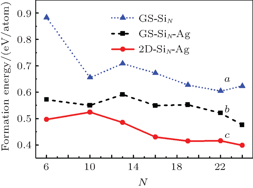 | Fig. 2. Formation energies of SiN clusters in vacuum and on Ag (111) surface: (a) freestanding SiN clusters with ground state configurations in vacuum (GS– SiN); (b) direct deposition of GS– SiN clusters on Ag (111) surface (GS– SiN– Ag); (c) 2D silicene-like clusters on Ag (111) surface (2D-SiN– Ag).[28] |
A recent study has demonstrated that the nucleation rate of silicene is very sensitive to both the growth temperature and the chemical potential Δ μ of the silicon atoms.[70] At a typical growth temperature (500 K), the nucleation rate showed a ∼ 23-orders of magnitude increase (from ∼ 10− 10 cm− 2· s− 1 to ∼ 1013 cm− 2· s− 1) as the Δ μ varies from 0.05 eV to 0.15 eV. For a specified Δ μ (e.g. Δ μ = 0.1 eV), reduction of the temperature from 500 K to 300 K would lead to an ∼ 11-orders of magnitude drop in the nucleation rate (from 107 cm− 2· s− 1 to 10− 4 cm− 2· s− 1). Usually, a high nucleation rate will result in a large number of defects. Thus, the growth conditions should be carefully chosen in order to reduce the defects in silicene.
As discussed above, defects are nearly inevitable in the growth of silicene. Hence, how defects affect the electronic properties of silicene becomes an important issue. Here we briefly discuss the geometries and stabilities of some point defects in a silicene monolayer, as well as the defect effect on the electronic properties of silicene, which have been comprehensively investigated by our group through using first-principles calculations.[56]
The geometries of various point defects in silicene, including Stone– Wales rotation, single and double vacancies (abbreviated as SW, SV, and DV, respectively, hereafter), and Si adatom are displayed in Fig. 3. Here, the formation energy is defined as EF = ET− N × ESi, where ET is the total energy of defective silicene, N is the number of silicon atoms in the supercell of defective silicene, and ESi is the energy per silicon atom in a perfect silicene sheet. For Stone– Wales rotation, two five-membered rings and two seven-membered rings are generated with a formation energy of 2.09 eV. The barrier for creating an SW defect is 2.64 eV, while the reverse barrier is as low as 0.5 eV, indicating that annealing at an appropriate temperature may eliminate the existing SW defects. Two kinds of SV defects are considered: SV-2 with three dangling atoms is less stable than SV-1 with (55| 66) rings. In the case of DV defects, two five-membered rings and one eight-membered ring are introduced. A reconstruction of DV defect with an energy barrier of 1.20 eV transforms (5| 8| 5) rings into (555| 777) and lowers the formation energy by 0.86 eV. Note that the formation energy for a DV is much smaller than that for two isolated SVs, which implies that two SVs may coalesce into a DV by diffusion. The DFT calculations showed that an SV-1 defect can migrate within the silicene sheet with a small energy barrier of 0.12 eV. Thus, the combination of two SVs into a DV is probable. In contrast, a large energy barrier (2.06 eV) would prevent the diffusion of DV-2. The Si adatom prefers the top site of silicene with the original lattice Si atom pressed down (Fig. 3(f)). To our surprise, the formation energy for Si adatom may even be negative.
Defects can effectively modify the electronic properties of silicene. SW and DV-1 (5| 8| 5) defects would introduce small band gaps of 33 meV and 161 meV in silicene, respectively. The SV-1 (55| 66) defect would transform semi-metallic silicene into metallic silicene. DV-2 (555| 777) would destroy the Dirac cone, but keep the semimetal characteristic of silicene. Most interestingly, an Si adatom not only opens a noticeable band gap of 91 meV but also induces a local magnetic moment of 2 μ B in silicene.
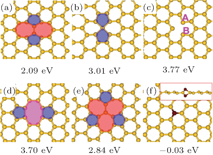 | Fig. 3. Geometries and formation energies of various point defects in silicene: (a) SW; (b) SV-1 by (55| 66) rings; (c) SV-2 with three dangling atoms; (d) DV-1 (5| 8| 5); (e) reconstructed DV-2 (555| 777); (f) Si adatom.[56] |
On the other hand, porous silicene with DV-1 and DV-2 defects are chemically inert to noble gases (He, Ne, and Ar), H2, H2O, CO, CO2, N2, and CH4 without additional hydrogen or nitrogen atoms to passivate the edge silicon atoms, showing a great prospect for gas purification.[71, 72] The diffusion energy barrier for H2 through the DV-1 of silicene is only about 0.34 eV, suggesting that an H2 molecule can permeate the porous silicene at moderate temperature and pressure.[71] The calculated diffusion energy barriers are 1.03, 0.99, 1.01, and 1.66 eV for N2, CO, CO2, and CH4, respectively. Therefore, a porous silicene sheet with DV-1 would serve as a good hydrogen purification membrane.[71] Moreover, a porous silicene sheet with DV-1 or DV-2 also exhibits high selectivities to He/Ne and He/Ar.[72]
So far, metal substrates, especially Ag (111), have been the most frequently used for silicene growth. Thus, understanding the interaction mechanism between silicene and the Ag substrate is significant for the fabrication and utilization of silicene. As shown in Fig. 4, a 2D Si24 cluster composed of seven hexagonal rings (which can be viewed as a small patch of silicene) is placed on an Ag (111) substrate and remains stable upon relaxation.[28] Strong hybridization between Si pz electrons and Ag 4d electrons is confirmed by the local density of states (LDOS) for Si24@Ag (111) (Fig. 4(b)), which shows that the 3p states of Si atoms couple with the 4d states of an Ag atom in the vicinity of the Fermi level. The strong p– d hybridization of Si– Ag can stabilize the silicene sheet on an Ag (111) surface, this is further supported by a recent Raman observation in experiment.[57] Moreover, such a strong hybridization may account for the vanishing of Dirac fermion characteristics of silicene on an Ag (111) surface, which will be discussed later. The charge differential densities of Si24@Ag (111) (Fig. 4(d)) illustrate that all Si atoms at both the peripheral and inner regions of an Si24 cluster interact evenly with the Ag (111) surface. The homogeneous interaction between silicon atoms and the Ag substrate is further supported by the homogeneous on-site charges of Si atoms in an Si24@Ag (111) system (Fig. 4(c)). Therefore, one can conclude that silicon atoms in silicene homogeneously interact with the Ag (111) surface, which is surely beneficial for the continuous growth of high-quality silicene.
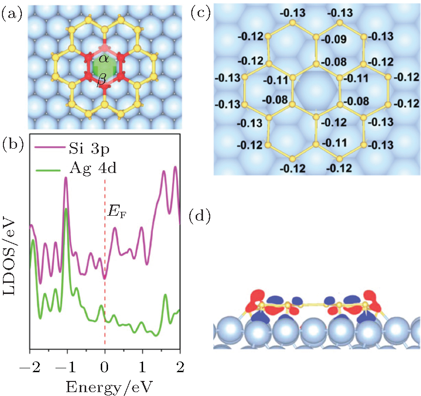 | Fig. 4. (a) Atomic structures, (b) local density of states (LDOS), (c) on-site Mulliken charges (| e| ), (d) charge differential densities of Si24@Ag (111) system. The LDOS comes from the central six silicon atoms (3p orbital) highlighted by red balls as well as the Ag atoms (4d orbital) highlighted by green ball right underneath the Si hexagon. In panel (d), red (blue) zone loses (gains) charge.[28] |
The interaction strength between silicene and the Ag substrate can be described by the binding energy, defined as

where Esi is the energy of silicene, Esub is the energy of the Ag substrate, and Et is the energy of silicene/Ag system. On the Ag (111) surface, the silicene sheet can form several superstructures, including (3× 3) silicene on (4× 4) Ag (111) surface (type I), 


The isolation of silicene from metallic substrates remains a big obstacle for the application of silicene, although recently highly buckled silicene has been synthesized on a semiconducting MoS2 substrate.[31] Recently, there has been a fierce debate about whether the Dirac cone of silicene can be preserved on an Ag (111) surface.[26, 73– 80] In 2012, linear dispersion coming from silicene was announced to be observed by angular-resolved photoelectron spectroscopy (ARPES) measurements in the type I superstructure with a Dirac cone about 0.3 eV below the Fermi level.[26] However, by combining spectroscopic signatures of quantum Hall effect by the Landau quantization under a magnetic field and DFT calculations, Lin et al. argued that silicene would lose its Dirac fermion character after being attached on a Ag (111) surface.[75] Recent DFT calculations have also shown that the Dirac cone of silicene is destroyed on the Ag (111) surface due to the strong interaction and mixing between Si and Ag orbitals, and the linear dispersions observed in experiments originate either from the Ag substrate or from the hybridization states between silicene and Ag (111) surface.[73– 77] Moreover, first-principles calculations suggest that the absence of the Dirac cone is a common feature for epitaxial silicene on metal substrates, including Ir, Cu, Mg, Au, Pt, Al, and Ag.[73] On the contrary, Avila et al. recently reported that the linear dispersion still comes from silicene, according to a compiled set of LEED, CLs, and ARPES data.[79]
For the real applications of silicene in microelectronic devices, silicene sheets must be placed on some insulating substrate. Therefore, how the insulating substrates affect the electronic properties of silicene becomes an important issue. So far, considerable efforts have been devoted to exploring the effect of insulating substrates on the electronic properties of silicene. Houssa et al. proposed that a silicene flake could preserve the semimetallic behavior when it is embedded between ultrathin insulating AlN layers.[41] SiC is frequently used in the microelectronics industry as an insulator and in graphene-based field effect transistor (FET).[81– 83] Meanwhile, h-BN monolayer is successfully fabricated in experiment[84] and is widely used as a substrate in graphene-based FET to improve the performance.[85– 88] Therefore, these two substrates have been frequently studied by first principle calculations to explore the substrate effect on silicene.[89– 91] The structures of silicene on h-BN and SiC are shown in Fig. 5. For SiC, two kinds of substrates are considered; i.e., Si-terminated SiC (0001) surface (Si– SiC) and C-terminated SiC (0001) surface (C– SiC). It is found that silicene preserves its geometric structure with a distance of about 3 Å from all these substrates. The cohesive energies between silicene and substrates are about 0.07 eV– 0.09 eV per silicon atom, which are the typical strengths of the van der Waals (vdW) interaction. Thus, these substrates can provide effective mechanical support for silicene without disturbing its geometrical structure.
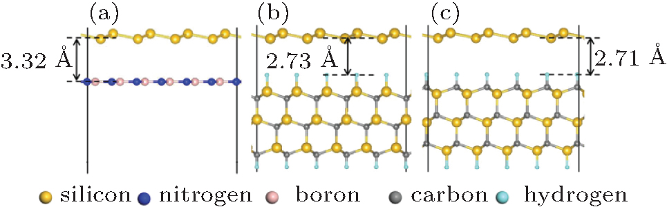 | Fig. 5. Atomic structures of silicene on: (a) h-BN; (b) Si– SiC; (c) C– SiC substrates.[89] |
The band structures of pristine silicene, silicene/BN, silicene/Si– SiC, and silicene/C– SiC are shown in Fig. 6. The Dirac cone in pristine silicene (highlighted by red lines) can be preserved after being placed on h-BN and Si– SiC. Actually, small band gaps of several meV are opened in silicene/BN and silicene/Si– SiC systems. For silicene/BN, several Moiré superstructures are studied and the band gap opened in the Fermi level reaches around 30 meV, which is nearly independent of the rotation angle between the two lattices.[90] The intact linear dispersion of silicene is also confirmed by the partial charge densities around the Fermi level. As shown in Figs. 6(f) and 6(g), the partial charge densities in an energy range from EF∼ EF − 0.2 eV are mainly distributed on silicene, indicating that the bands around the Fermi level are all from silicene. In sharp contrast, the π -bands of silicene are severely disturbed by C– SiC substrate and silicene becomes n-doped (Fig. 6(d)). The partial charge densities (Fig. 6(h)) clearly show that the valence bands of C– SiC already enter into the vicinity of the Fermi level of the silicene/C– SiC hybrid system.
The different substrate effects on the electronic properties of silicene can be attributed to the relative locations of valence band maximum (VBM) and conduction band minima (CBM) of silicene and substrates. The CBM (or VBM) of silicene is 0.1 eV lower than the VBM of C– SiC substrate. Owing to the interaction between silicene and C– SiC substrate, some new electronic states in the energy range between the VBM of C– SiC and that of silicene arise, thus lowering the total energy of the hybrid system. After the combination of silicene and C– SiC substrate, the Fermi energy of the hybrid system will stay between the VBM of C– SiC and the VBM of silicene. Hence, the Dirac cone of the pristine silicene is submerged under the Fermi level. While for the silicene/BN and silicene/Si– SiC systems, the CBM of silicene is located in the gap region between BN and Si– SiC. The electronic states ranging between the VBM of Si– SiC (or BN) and the CBM of silicene are forbidden. Consequently, the conical point of the Dirac cone in silicene is basically retained at the Fermi level.
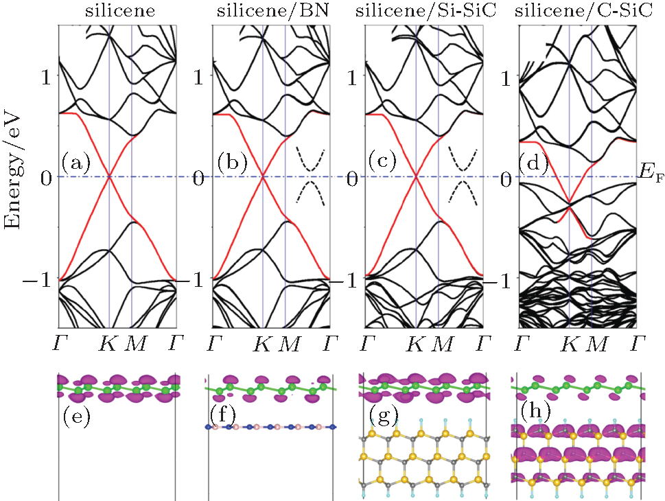 | Fig. 6. Electronic band structures of (a) silicene, (b) silicene/BN, (c) silicene/Si– SiC, (d) silicene/C– SiC and partial charge densities of (e) silicene (f) silicene/BN, (g) silicene/Si– SiC, (h) silicene/C– SiC. The red lines highlight the π -bands of silicene in different configurations. The partial charge densities are in an energy range from EF∼ EF to 0.2 eV. The Fermi level is set to be zero. The enlarged view of the band lines at K point near the Fermi level is presented in the inset.[89] |
In addition to SiC and h-BN, many other insulating or semiconducting substrates, including MoS2, MoSe2, MoTe2, silicane, Cl-silicene, Br-silicene, graphane, solid argon, MgX2 (X = Cl, Br, and I), hydrogenated Si (111) surface, hydrogenated Ge (111) surface, GaS, GaSe, and GaTe, have been considered as possible supports of silicene.[91– 99] First-principles calculations show that all of these substrates can provide effective mechanical support without destroying the geometric and electronic structures of silicene and result in small band gaps from tens to more than one hundred meV. All of these substrates have inert surfaces without any dangling bonds and thus interact with silicene through weak vdW interactions, which is responsible for the preservation of the geometry and electronic structures of silicene. However, if there are dangling bonds on the surface of substrates, then the unique electronic properties of silicene would be destroyed. For example, silicene loses its linear dispersion around the Fermi level when it is placed on ZnS (0001) surface and the hybrid system is predicted to be semiconducting with an indirect gap of about 0.7 eV.[100] The electronic properties of pristine silicene would be badly destroyed when epitaxially grown on (111) surfaces of AlAs, AlP, GaAs, GaP, ZnS, and ZnSe.[101] Small band gaps arise due to the symmetry breaking of two sublattices in silicene.
The dispersion relation of silicene near Fermi level can be described by using a tight-binding model:[102]

where k is the wavevector relative to Dirac point, ν F is the Fermi velocity, and Δ represents the on-site energy difference between electrons at the two sublattices. Accordingly, the band gap of silicene/substrate superstructures Eg = 2Δ . Van der Waals interactions yield small Δ and thus small band gap. According to this, the band gap created at the Dirac point may be further tuned by the interaction strength between silicene and substrates or bias voltage. A recent study has predicted that the band gap increases with reducing the interlayer distance between silicene and h-BN.[90] Moreover, the band gaps of silicene/MoS2, [92, 93] silicene/MgX2 (X = Cl, Br, and I), [96] silicene/silicane, [97] and silicene/GaS[99] systems can be effectively modulated by an external electric field perpendicular to the interface.
Without a substrate, free-standing monolayer silicene is unstable due to its high formation energy and active surface.[56] Moreover, monolayer silicene is a zero gap semimetal, which certainly hinders its applications in microelectronics and optoelectronics. It is generally known that stacking is a universal method to modulate properties of 2D materials and may offer new opportunities to open a band gap.[103, 104] Multilayer silicene has been successfully synthesized on an Ag (111) surface by the epitaxial technique in recent experiments.[25, 32– 35] For the as-prepared multilayer silicene, the bottom layer (bonded with Ag surface) usually exhibits a (3× 3) superstructure with respect to free-standing silicene. 

On the theoretical side, significant efforts have been devoted to bilayer silicene and in total six kinds of bilayer silicene have been brought forward.[105– 114] Five possible structures of bilayer silicene, namely, planar bilayer silicene (P-BS), AB-stacked bilayer silicene (AB-BS), AA-stacked bilayer silicene (AA-BS), AA′ -stacked bilayer silicene (AA′ -BS), and slide-AA bilayer silicene (slide-AA-BS), are shown in Fig. 7. Indeed, the search for the most stable structure of bilayer silicene can be traced back to 2008.[105] By quenching liquid silicon confined in slit nanopores through using molecular-dynamics (MD) calculations with the Tersoff potential, Morishita et al. predicted the formation of AA′ -BS.[105] P-BS was first proposed by Bai et al. in 2010 via MD simulations.[107] Subsequently, these five kinds of bilayer silicene are all constructed by stacking two silicene layers, [108– 112] and their stability and electronic properties have been systematically investigated.[109, 113] Recent DFT calculations combined with the particle swarm optimization algorithm have predicted a new silicene bilayer structure, called Si-Cmme, with lower energy than the widely accepted lowest energy configuration (P-BS).[114]
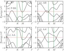
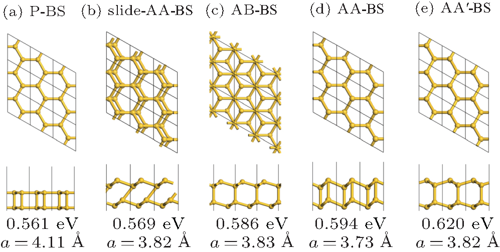 | Fig. 7. Atomic structures (upper for top view, lower for side view) of various silicene bilayers along with formation energies per Si atom and lattice constants. The black lines highlight the primitive cell of bilayer silicene.[113] |
For P-BS, AA-BS, and AA′ -BS, the two silicene layers coincide from the top view. The two silicene layers are planar in P-BS, but buckled in AA-BS and AA′ -BS. In AA-BS, the lower atoms in the first layer are located right above the lower atoms in the second layer, while in AA′ -BS, the lower atoms in the first layer are located right above the upper atoms in the second layer. In slide-AA-BS, silicon atoms in the upper layer are not directly located on the top sites of lower atoms but slightly off the exact AA stacking.[109] AB-BS is indeed a slab model of an Si (111) surface. Two silicene layers bond together covalently for all the six stacking patterns, which is different from the bilayer graphene with a vdW interlayer interaction only.[115]
According to the formation energy, P-BS is stablest in all bilayer systems, except for Si-Cmme. Interestingly, P-BS is 0.025 eV/atom, which is even stabler than the slab model of Si (111) surface; i.e., AB-BS, suggesting that a phase transition will occur when the silicon film becomes as thin as only two-layers. Indeed, the strain-induced phase transition from AB-BS to P-BS was recently reported.[108]
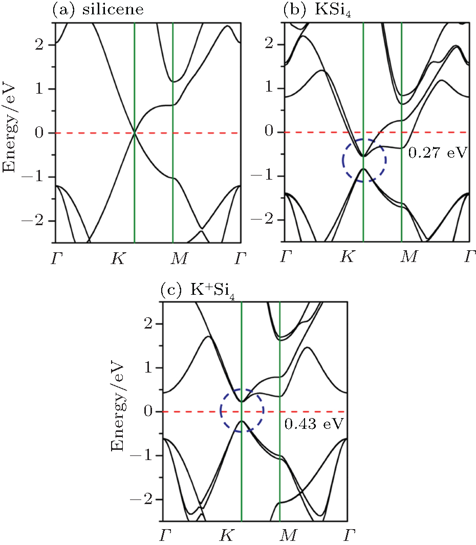
Bilayer silicene systems distinctly show different electronic properties depending on the stacking style.[106, 107, 109– 112] Unlike bilayer graphene, the Dirac cone in pristine silicene is badly destroyed in bilayer silicene due to the strong interaction between two silicene layers. The band structures calculated with PBE functional for P-BS, AB-BS, AA-BS, and AA′ -BS are shown in Fig. 8. The P-BS exhibits metallic character with an indirect overlap between the CBM and VBM (Fig. 8(a)). For AB-BS, two parabolic bands cross the Fermi level (Fig. 8(b)) AA-BS exhibits apparent metallic feature with several bands crossing the Fermi level (Fig. 8(c)). For AA′ -BS, two crossings of nearly linear dispersions emerge along two directions, namely G– K and G– M (Fig. 8(d)). One crossing point is slightly above the Fermi level (by 70 meV), and another one is right below the Fermi level (by 65 meV). The newly found Si-Cmme is also metallic.[114] In particular, the band structure calculated with Heyd– Scuseria– Ernzerhof (HSE) hybrid functional suggests that slide-AA-BS is an indirect semiconductor with a band gap of 1.16 eV.[109]
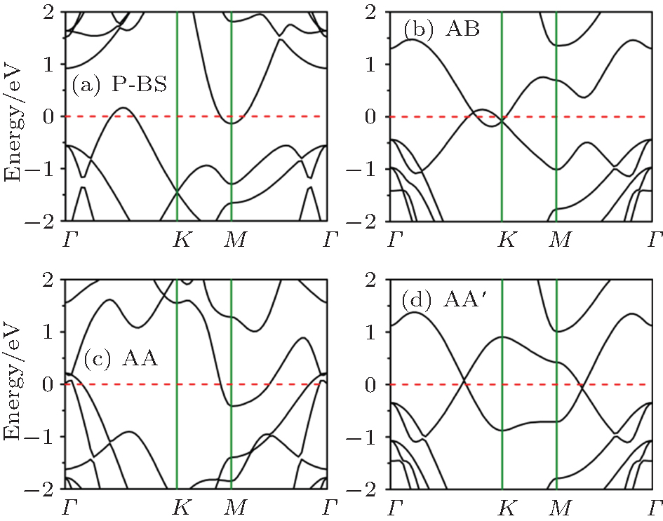 | Fig. 8. Band structures of four bilayer silicene sheets: (a) P-BS, (b) AB-BS, (c) AA-BS, and (d) AA′ -BS.[113] |
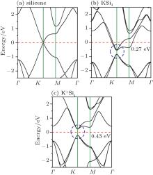
The absence of a Dirac cone in bilayer silicene no doubt hinders their utilization in future microelectronic devices. Fortunately, an effective method, potassium intercalation, has been proposed to decouple the strong interactions between two silicene layers, thus recovering the superior electronic properties of silicene.[113] As displayed in Fig. 9, bilayer silicene sheets intercalated with alkali metal atom (including Li, Na, K, and Rb), namely, LiSi4, NaSi4, KSi4, and RbSi4, are systematically investigated by first-principles calculations.[113] After intercalation, two silicene layers are separated with an interlayer distance larger than 3.8 Å and the low buckled structure of pristine silicene is basically recovered. Moreover, the formation energies of LiSi4, NaSi4, KSi4, and RbSi4 are 0.275 eV, 0.302 eV, 0.309 eV, and 0.507 eV per atom, respectively, which are lower than that of P-BS (0.561 eV per atom) and much lower than that of free-standing silicene (0.779 eV per atom). The ab initio molecular dynamics (AIMD) simulation at 500 K confirms the thermal stability of KSi4. Most importantly, the feature of Dirac cone of silicene is restored after intercalation. For KSi4, a double-degenerated Dirac cone with a band gap of 0.27 eV appears at the K point in the first Brillouin zone (Fig. 10(b)). However, the band gap is submerged under the Fermi level due to the charge transfer from K atoms to silicene. The Fermi level can be lifted up by replacing the neutral potassium atom with its cation (K+ ). As displayed in Fig. 10(c), the band structure of K+ Si4 exhibits a semiconducting character with a moderate gap of 0.43 eV. In an FET device, the charge doping of this type can be realized by applying a suitable gate voltage.[116]
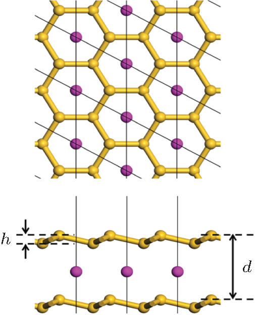 | Fig. 9. Atomic structure of alkali metal intercalated bilayer silicene (upper for top view, lower for side view). The yellow balls represent silicon atoms and the purple balls represent alkali metal atoms. The black lines define the primitive cell with four silicon atoms and one metal atom.[113] |
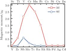
The 2D magnetic materials are important for developing spintronics and magnetic storage. Ferromagnetism can be induced in silicene by half hydrogenation[44, 45] or direct adsorption of transition metal adatoms.[50, 53] However, ordered phase is hard to form in these systems since the transition metal atoms tend to aggregate. Recently, seven monolayers of transition metal silicides (TMSi2), namely., TiSi2, VSi2, CrSi2, MnSi2, FeSi2, NbSi2, and MoSi2, with magnetic orders were reported by our group.[117] These monolayer silicides can be constructed by placing a transition metal atom in the center of each hexagonal hole of honeycomb lattice of silicene, as shown in Fig. 11. Among them, TiSi2, CrSi2, MnSi2, and FeSi2, are planar (Fig. 11(a)), while VSi2, NbSi2, and MoSi2 are buckled (Fig. 11(b)).
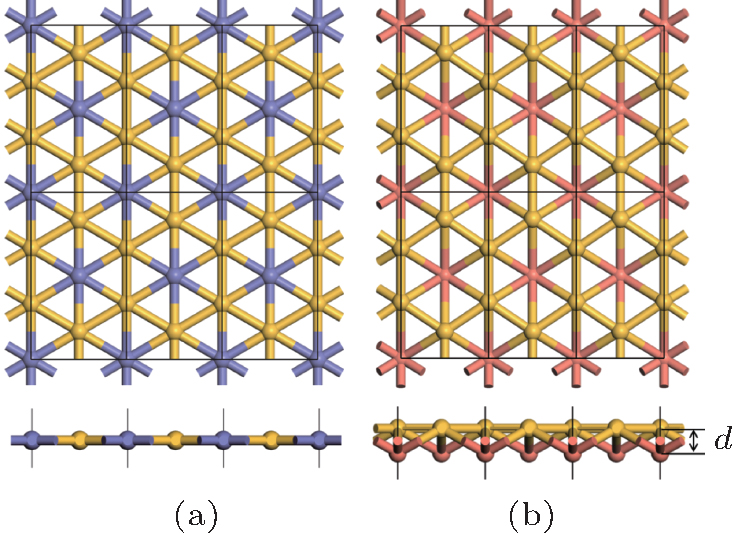 | Fig. 11. Top views and side views of (a) planar monolayers of TiSi2, CrSi2, MnSi2, and FeSi2; (b) buckled monolayers of VSi2, NbSi2, and MoSi2. The blue or red balls represent transition metal atoms and the yellow balls represent silicon atoms. The black rectangle represents the unit cell. The values of buckled height (d) for VSi2, NbSi2, and MoSi2 are 0.289, 0.756, and 0.647 Å respectively.[117] |
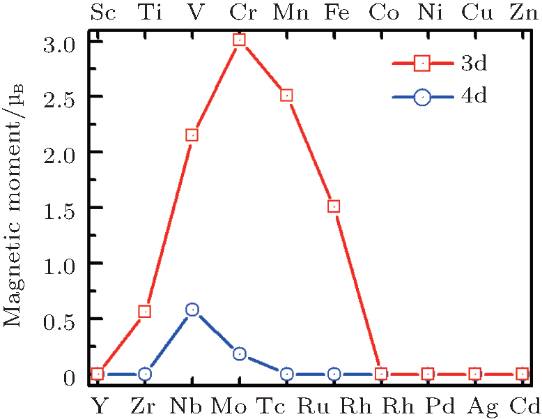 | Fig. 12. Magnetic moments per 3d or 4d atom of TMSi2 silicide monolayer. The red line represents 3d silicide and the blue line represents 4d one.[117] |
Compared with the atomic spins of 2, 3, 6, 5, 4, 1, and 2 μ B for individual Ti, V, Cr, Mn, Fe, Nb, and Mo atoms, respectively, the magnetic moment per TM atom in the TMSi2 monolayers is reduced by about half. As shown in Fig. 12, the on-site moments per TM atom in the TMSi2 monolayers are 0.563, 2.148, 3.008, 2.512, 1.508, 0.618, and 0.207 μ B for Ti, V, Cr, Mn, Fe, Nb, and Mo, respectively, while the remaining 3d and 4d TMSi2 monolayers are all non-magnetic. Among all of the magnetic systems, TiSi2, VSi2, CrSi2, NbSi2, and MoSi2 exhibit ferromagnetic ordering, while MnSi2 and FeSi2 monolayers favor antiferromagnetism. Among them, the formation energies of ferromagnetic TiSi2 and antiferromagnetic FeSi2 monolayers are lower than that of silicene, and the formation energy of antiferromagnetic MnSi2 with large on-site moment is comparable to that of silicene. As a result, these three TMSi2 monolayers are expected to possibly be synthesized in experiments due to their low formation energies. An outstanding advantage of these novel TMSi2 monolayers is the tunable magnetic ordering from ferromagnetic to antiferromagnetic, implying their great potential in future spintronic devices.
In this review, the growth behavior, effects of defects and substrates, and bilayer silicene are discussed. The wetting of the Ag (111) surface is crucial for silicene growth, since small silicon clusters prefer 2D structures due to passivation of the Ag atoms. Moderate and homogeneous interaction between silicene and the Ag (111) surface accounts for the superiority of Ag substrate for silicene growth. Defects, which are nearly inevitable in the fabrication, would greatly affect the electronic properties of silicene, either opening a small band gap or transforming it into metal. Moreover, porous silicene sheets with double vacancies are promising for gas purification.
After being synthesized on a metal surface, silicene is very likely to lose its Dirac cone due to strong hybridization between silicene and substrate, although there is still some debate about this point. Excitingly, many inert substrates (semiconductor or insulator) can afford effective mechanical support without destroying the geometric and electronic properties of silicene. Furthermore, a small band gap can be opened in silicene supported on these inert substrates due to the weak vdW interactions which break the symmetry of the two sublattices in silicene.
Bilayer silicene has a lower formation energy than monolayer silicene but loses the Dirac cone due to the strong covalent interaction between two silicene layers. Alkali metal intercalation can effectively decouple the two silicene layers, thus restoring the Dirac cone in pristine silicene with a small band gap at the vertex of the Dirac cone. Besides, alkali metal intercalation can further lower the formation energy compared with bilayer silicene, making intercalated bilayer silicene a promising prospective in future microelectronic devices, especially FET. As an extension of silicene, some monolayers of transition metal silicides are ferromagnetic or antiferromagnetic, which is useful in future spintronic devices.
Even though the use of silicene is promising in many applications, the research of silicene still has a long way to go. Various superstructures of silicene coexist during the epitaxial growth and thus a large number of structural defects and grain boundary emerge in the epitaxial silicene sheets. Fabricating large-scale defect-free silicene with a uniform superstructure is still a considerable challenge. Transferring silicene from metal substrates onto inert substrates without destroying the structural integrity of the 2D sheet is another difficult issue. Alternatively, one may try to grow silicene directly on some inert substrates. Recent success in building a silicene field-effect transistor has introduced a new and effective method of developing silicene-based microelectronic devices. Optimistically, all of these problems might be overcome in the near future, which will in turn open a bright future for silicene in future microelectronics and other nanoscale devices.
| 1 |
|
| 2 |
|
| 3 |
|
| 4 |
|
| 5 |
|
| 6 |
|
| 7 |
|
| 8 |
|
| 9 |
|
| 10 |
|
| 11 |
|
| 12 |
|
| 13 |
|
| 14 |
|
| 15 |
|
| 16 |
|
| 17 |
|
| 18 |
|
| 19 |
|
| 20 |
|
| 21 |
|
| 22 |
|
| 23 |
|
| 24 |
|
| 25 |
|
| 26 |
|
| 27 |
|
| 28 |
|
| 29 |
|
| 30 |
|
| 31 |
|
| 32 |
|
| 33 |
|
| 34 |
|
| 35 |
|
| 36 |
|
| 37 |
|
| 38 |
|
| 39 |
|
| 40 |
|
| 41 |
|
| 42 |
|
| 43 |
|
| 44 |
|
| 45 |
|
| 46 |
|
| 47 |
|
| 48 |
|
| 49 |
|
| 50 |
|
| 51 |
|
| 52 |
|
| 53 |
|
| 54 |
|
| 55 |
|
| 56 |
|
| 57 |
|
| 58 |
|
| 59 |
|
| 60 |
|
| 61 |
|
| 62 |
|
| 63 |
|
| 64 |
|
| 65 |
|
| 66 |
|
| 67 |
|
| 68 |
|
| 69 |
|
| 70 |
|
| 71 |
|
| 72 |
|
| 73 |
|
| 74 |
|
| 75 |
|
| 76 |
|
| 77 |
|
| 78 |
|
| 79 |
|
| 80 |
|
| 81 |
|
| 82 |
|
| 83 |
|
| 84 |
|
| 85 |
|
| 86 |
|
| 87 |
|
| 88 |
|
| 89 |
|
| 90 |
|
| 91 |
|
| 92 |
|
| 93 |
|
| 94 |
|
| 95 |
|
| 96 |
|
| 97 |
|
| 98 |
|
| 99 |
|
| 100 |
|
| 101 |
|
| 102 |
|
| 103 |
|
| 104 |
|
| 105 |
|
| 106 |
|
| 107 |
|
| 108 |
|
| 109 |
|
| 110 |
|
| 111 |
|
| 112 |
|
| 113 |
|
| 114 |
|
| 115 |
|
| 116 |
|
| 117 |
|