


Modulation of electronic properties with external fields in silicene-based nanostructures
[Li Genga), b) , Zhao Yin-Changa), b) , Zheng Ruia), b) , Ni Jun†a), b)  , Wu Yan-Ning
c) ]
, Wu Yan-Ning|
|


†Corresponding author. E-mail: junni@mail.tsinghua.edu.cn
*Project supported by the National Natural Science Foundation of China (Grant Nos. 11374175 and 11174171).
This work reviews our recent works about the density functional theory (DFT) calculational aspects of electronic properties in silicene-based nanostructures with the modulation of external fields, such as electric field, strain, etc. For the two-dimensional (2D) silicene-based nonostructures, the magnetic moment of Fe-doped silicene shows a sharp jump at a threshold electric field, which indicates a good switching effect, implying potential applications as a magnetoelectric (ME) diode. With the electric field, the good controllability and sharp switching of the magnetism may offer a potential applications in the ME devices. For the one-dimensional (1D) nanostructures, the silicene nanoribbons with sawtooth edges (SSiNRs) are more stable than the zigzag silicene nanoribbons (ZSiNRs) and show spin-semiconducting features. Under external electric field or uniaxial compressive strain, the gapless spin-semiconductors are gained, which is significant in designing qubits for quantum computing in spintronics. The superlattice structures of silicene-based armchair nanoribbons (ASiSLs) is another example for 1D silicene nanostructures. The band structures of ASiSLs can be modulated by the size and strain of the superlattices. With the stain increased, the related energy gaps of ASiSLs will change, which are significantly different with that of the constituent nanoribbons. The results suggest potential applications in designing quantum wells.
Graphene, a two-dimensional (2D) honeycomb lattice of carbon, has attracted significant interests in exploring the rich condensed-matter physical phenomena since its experimental realization.[1] So far, many exceptional features such as high strength of the lattice structure, massless Dirac fermions, high thermal conductivity, and half-integer Hall conductance have been revealed for this atomically thin layers.[2– 6] Also its remarkable and exotic chemical and physical properties have aroused interests in other elements and molecules that form of 2D atomic layers, such as silicon, [7– 10] germanium, [7– 9, 11] etc. Similar to graphene, silicene, the counterpart of network for silicon, has a honeycomb geometry and low-buckled structure.[5, 7, 12, 13] Because of its similarities to graphene and additional advantages, it becomes one of the hottest material in basic scientific research and nanoelectronic devices applications.[10, 14– 18]
Pristine silicene favors to form stable, two-dimensional, low-buckled honeycomb structures, where exists two sublattices that are not in the same plane with a buckled height of about 0.46 Å .[7, 19– 21] Compared to the complete sp2 hybridization between the C– C bonds in graphene, [6] the Si– Si bonds in silicene prefer to form the mixing of sp3-hybridized orbitals and sp2 planar bonds.[22] Given a relative large spin– orbit coupling in silicene, a band gap of 1.55 meV can be opened, which gives rise to unique phenomena such as the anomalous quantum Hall effect, quantum spin Hall effect, and unexpected magnetic ordering.[23– 26] Similar to graphene, its band structures show linear band crossing at the Fermi level and thus have Dirac points at the K and K0 points of the hexagonal Brillouin zone (BZ).[27– 30] So, the charge carriers near the Fermi level in silicene, like the massless Dirac fermions, can move with a velocity of 105 m/s– 106 m/s.[27– 30] When a single layer silicene is subjected to a perpendicular external magnetic field, a valley-polarized quantum Hall effect appears.[26, 30, 31] Furthermore, according to recent theoretical studies, 2D topological insulating characteristics of silicene is explored.[23, 24, 26]
Except for the silicene sheet, the other two Si-based nanostructures — silicon nanotubes and silicene nanoribbons — have also been fabricated and investigated. Before the fabrication of large-scale silicene, graphene-like silicene nanoribbons were successfully synthesized on Ag (001) and Ag (110) surfaces, [32– 35] respectively and silicon nanotubes with a hollow structure have also been reported to be grown from silicon monoxide.[36] For Si nanotube, our first-principles calculations show that the surfaces of nanotubes are buckled with Si atoms having different distances to the axis of the tube and the silicon nanotubes with a large diameter are all semiconductors.[37] One-dimensional (1D) silicene nanoribbons (NRs) exhibit distinct electronic and magnetic properties depending on their chirality, width, and edge structure. First-principles calculations show that similar to graphene nanoribbons (GNRs), SiNRs with the armchair edges (ASiNRs) are semiconductors, and those with zigzag edges (ZSiNRs) have stable antiferromagnetic states, which become half-metals under a suitable external transverse electric field.[38– 42] Ding et al. found that the band gap of edge hydrogenated armchair silicene nanoribbons oscillates with the width in a period of three.[42] The excellent transport properties of silicene nanoribbons have also been studied theoretically.[43– 47] For example, Kang et al., using first principles calculations, studied the symmetry-dependent transport properties and magnetoresistance effect in silicene nanoribbons.[45] Many approaches, such as applying stress and strain, applying external electronic field, chemical decorating, and making defects (doping atom and vacancies), [48] have been used to tune the structural, energetic, magnetic, and electronic properties of pristine silicene and its nanostructures. Since silicene and silicene nanoribbons are obtained through growth on the substrate, the strain inevitably has an impact on the structural and electronic properties of these nanostructure.[49] A perpendicular electric field can induce a tunable band gap in silicene by breaking the inversion symmetry.[50] For example, under transverse electric field, semimetallicity can also be realized in zigzag silicene nanoribbons.[50] The adsorption of atoms and several common gas molecules on silicene is an effective way of functionalizing silicene nanostructures.[51, 52] The most stable configurations, the corresponding adsorption energies, charge transfer, and electronic properties of metal and several common gas molecules on silicene are thoroughly discussed by DFT. Nanostructures adsorbed with metal atoms may be applied for superconductivity, [53] hydrogen storage, [54– 56] catalyst, [57, 58] as well as tuning the electronic and magnetic properties.[52] Experiments and theories have shown that the existence of the defects, such as Stone– Wales defects (a 5– 7-member ring topological defect), [59] vacancies, [54, 60, 61] and substitutions, [62, 63] etc., can drastically change the electronic and magnetic properties of the silicene nanoribbons. The effects of these defects depend on their symmetry, repeating periodicity, and positions relative to the edge of the nanoribbon.[54] In addition, alkali metal intercalation and substrate– silicene interaction can also tune the electronic properties of silicene.[64, 65] These spin-dependent properties show that silicene-based nanostructures have potential applications in spintronic devices based on silicon materials.
The remainder of the paper is organized as follows. In Section 2, we show the spin-semiconducting properties of silicene nanoribbons with sawtooth edges (SSiNRs). Section 3 presents the extraordinary magnetic properties of the silicene doped with Fe and Cr metal atoms under external electric field. In Section 4, the various types of superlattice structures of silicene-based armchair nanoribbons (ASiSLs) which are the periodically repeated junctions made of ASiNRs with different widths, are discussed. Section 5 is the summary.
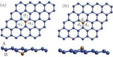
Using Lieb’ s theorem, [66] and a unified geometric rule, [67] two kinds of novel SiNRs can be constructed. They are called as Christmas-tree silicene nanoribbons (CSiNRs) and tree-saw silicene nanoribbons (TSiNRs), respectively, as shown in Fig. 1(a). Two integers (n1, n2) are utilized to label the size of the primitive cell. The two integers are the numbers of hexagonal rings along the n1 and n2 directions for CSiNRs, while n1 is the number of continuous zigzag chains and n2 is the number of hexagonal rings along the n2 direction for TSiNRs, as is shown in Fig. 1(a). CSiNRs or TSiNRs of size (n1, n2) are denoted as C(n1, n2) or T(n1, n2) simply. Using first-principles calculations, the electronic properties of the TSiNRs and CSiNRs are investigated.[68]
The stabilities of the SSiNRs can be identified from the formation energies of SSiNRs. The definition of the formation energies is Ef = (Etotal − nSiESi − nHEH)/(nSi + nH). ESi and EH are the energies of an isolated silicon atom and a single hydrogen atom, respectively. Etotal is the total energy of SiNRs. For comparison, The SSiNRs, ASiNRs, and ZSiNRs are all passivated with the same count ratio of silicon-to-hydrogen atoms (NSi/NH). As can be seen in Fig. 1(b), the formation energies of ASiNRs (AGNRs), ZSiNRs (ZGNRs), CSiNRs (CGNRs), TSiNRs (TGNRs) always reduce with increasing the value of NSi/NH (NC/NH). In other words, the nanoribbons with larger values of NSi/NH (NC/NH) are more stable than those with smaller NSi/NH (NC/NH) values. For a given value of NSi/NH, the formation energies of the CSiNR and TSiNR are lower than those of ZSiNR but higher than those of ASiNR. It indicates that the CSiNR and TSiNR are more stable than ZSiNR but less stable than ASiNR. In contrast, the two kinds of sawtooth graphene nanoribbons (SGNRs) are less stable than both zigzag and armchair graphene nanoribbons (ZGNRs and AGNRs).
The DFT calculations show the energy difference between the ferromagnetic (FM) state and nonmagnetic (NM) state is about 100 meV per unit cell, which indicates the ground states of SSiNRs favor to be ferromagnetic (FM) with a 2-μ B magnetic moment. Figure 2 shows that the ferromagnetic magnetism is localized on the two edges for both kinds of SSiNR. The ground state band structures are shown in Fig. 3(a) and Fig. 4(b) for C(5, 4) and T(5, 3), respectively, with one
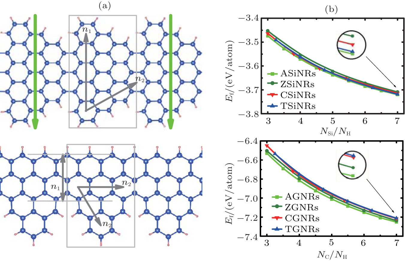 | Fig. 1. (a) Structures of a Christmas-tree silicene nanoribbon (CSiNR) (top) and a tree-saw silicene nanoribbon (TSiNR) (bottom). (n1, n2) denotes the size of the structures. The unit cells are marked by the gray rectangle lines. The downward bold gray (green) arrow labels the transverse electric field Eext applied across the CSiNR. (b) The formation energies versus the value of NSi/NH (NC/NH) for silicene nanoribbons (graphene nanoribbons). The square, circle, del, and triangular lines represent the Ef of ASiNRs (AGNRs), ZSiNRs (ZGNRs), CSiNRs (CGNRs), and TSiNRs (TGNRs), respectively.[68] |
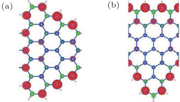 | Fig. 2. Distributions of charge density of spin-up state minus spin-down state for (a) C(5, 4) and (b) T(5, 3), respectively. The black (red) and gray (green) color label the spin-up and spin-down charges, respectively.[68] |
 | Fig. 3. (a) Band structures and charge distributions of the edge bands V1, V2, C1, and C2 for C(5, 4) without electric field. (b) Same as panel (a) but under Eext = 0.047 V/Å . The right-band structure is the enlargement of the left one. Panels (c) and (d) are the charge distributions of the four edge bands for T(5, 3) with electric field Eext = 0 and 0.049 V/Å , respectively. In band structures the black (red) and dark gray (blue) color denote the majority and minority spin states, while in charge distribution pictures the black (red) and gray (green) color label the majority and minority spin charges, respectively. (e) Energy gap of C(5, 4) and T(5, 3) as a function of Eext. Inset shows the gap of C(5, 4) near Eext = 0.[68] |
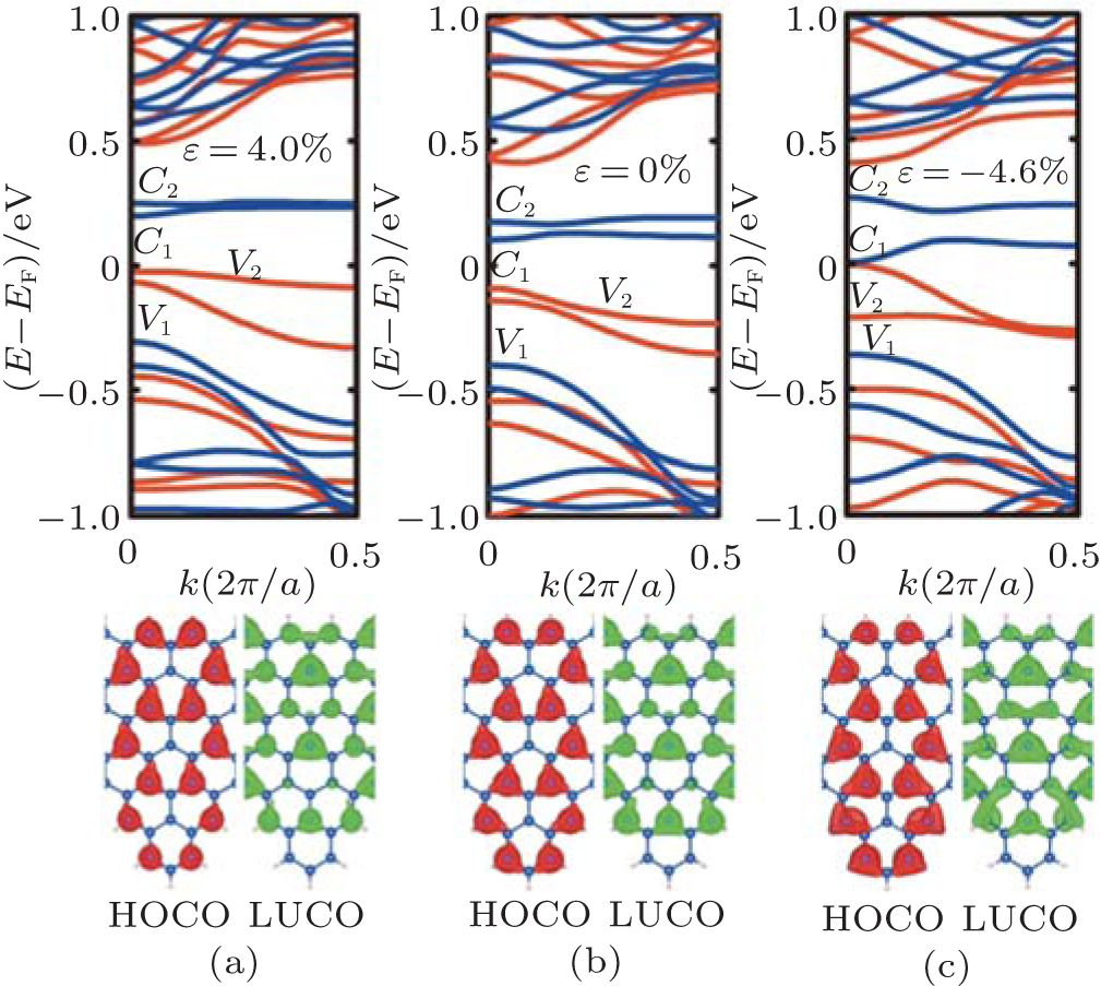 | Fig. 4. Band structures and partial charge densities of the lowest unoccupied crystal orbital (LUCO) and the highest occupied crystal orbital (HOCO) for the T(5, 3) structure with the strain of (a) ɛ = 4.0%, (b) ɛ = 0.0%, and (c) ɛ = − 4.6%. In band structures the black (red) and dark gray (blue) color denote the majority and minority spin states, respectively.[68] |
couple of spin-up bands (C1, C2) above Fermi level and another couple (V1, V2) below the Fermi level. The two couples of bands originate from the edge states.[69– 71] Between bands of V2 and C1 in C(5, 4) and T(5, 3) there is an intrinsic energy gap Egap of 0.25 eV and 0.19 eV, respectively. It proves that the SSiNRs are spin semiconductors. The distribution of magnetism of SSiNRs are mainly due to the antiferromagnetic property of primitive silicene and the edge-effect.
By applying a suitable transverse electric field, the band structure of SSiNRs are modulated and they become gapless spin semiconductors. The direction of the external electric field Eext is labeled in Fig. 1(a). Under Eext, the edge bands with identical spins split, and the gap Egap between the V2 and C1 bands become small. The gap of C(5, 4) (T(5, 3)) vanishes at Eext = 0.047 V/Å (Eext = 0.049 V/Å ), as depicted in Figs. 3(b) and 3(e). The carriers (electrons or holes) near the Fermi level transport in different spin states. Figure 3(e) shows the band gap changes with the Eext changing from 0 to 0.05 V/Å for C(5, 4) and T(5, 3), respectively. The results of the Eext inducing zero gap show that the wider SSiNRs are, the weaker Eext is needed. Figure 3(a) shows that the charge of each edge band in the CSiNRs localizes on both sides. But when Eext = 0.047 V/Å , the distribution varies with V1 and C1 bands localizing on the bottom edge while V2 and C2 on the top edge, as shown in Fig. 3(b). Figure 3(c) presents that the charges of V1 and C2 in TSiNRs localize on the top edge while V2 and C1 in TSiNRs on the bottom edge at Eext = 0. When Eext = 0.049 V/Å , the charge distribution of each band of V1 and V2 becomes localized on both edges, but the distribution of C1 and C2 remain unchanged, as is shown in Fig. 3(d). This charge separation in real space indicates that carriers transport along fixed edges according to their energy and spin states.
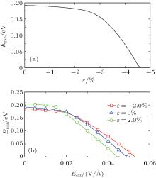
In addition, the role of the uniaxial strain along the periodic direction for the the electronic properties of SSiNRs is investigated.[70– 74] The gap Egap decreases slightly under compressive strain. For CSiNRs this wrinkle state is metastable and its band structure has a little change under the strain. However, the electronic properties of TSiNRs tuned by the compressive strain is interesting. Under the compressive strain, the edge bands broaden, the Egap reduces and the system tends to behave the spin gapless semiconducting feature. For example, the T(5, 3) becomes the spin gapless semiconductor at ɛ = − 4.6%, as presented in Figs. 4(c) and 5(a). Different from the case of applying Eext, the conduction and valence band converge at the Γ point when the gap becomes to zero induced by the compressive strain. However, the distribution of charge density of the V1, V2, C1, and C2 bands under strain is almost same to that induced by Eext. The distribution of charge density at the strain ɛ = − 4.6% is plotted in Fig. 3(d), same as that applying Eext = 0.049 V/Å . It is evident that electrons on the C1 band transport only in the spin-down state along the bottom edge while holes on the V1 band transport along both edges. Thus, when TSiNRs is modulated by Eext or compressive strain, the charge separation in real space is semi-separated, which is different from that in CSiNRs under electric field.
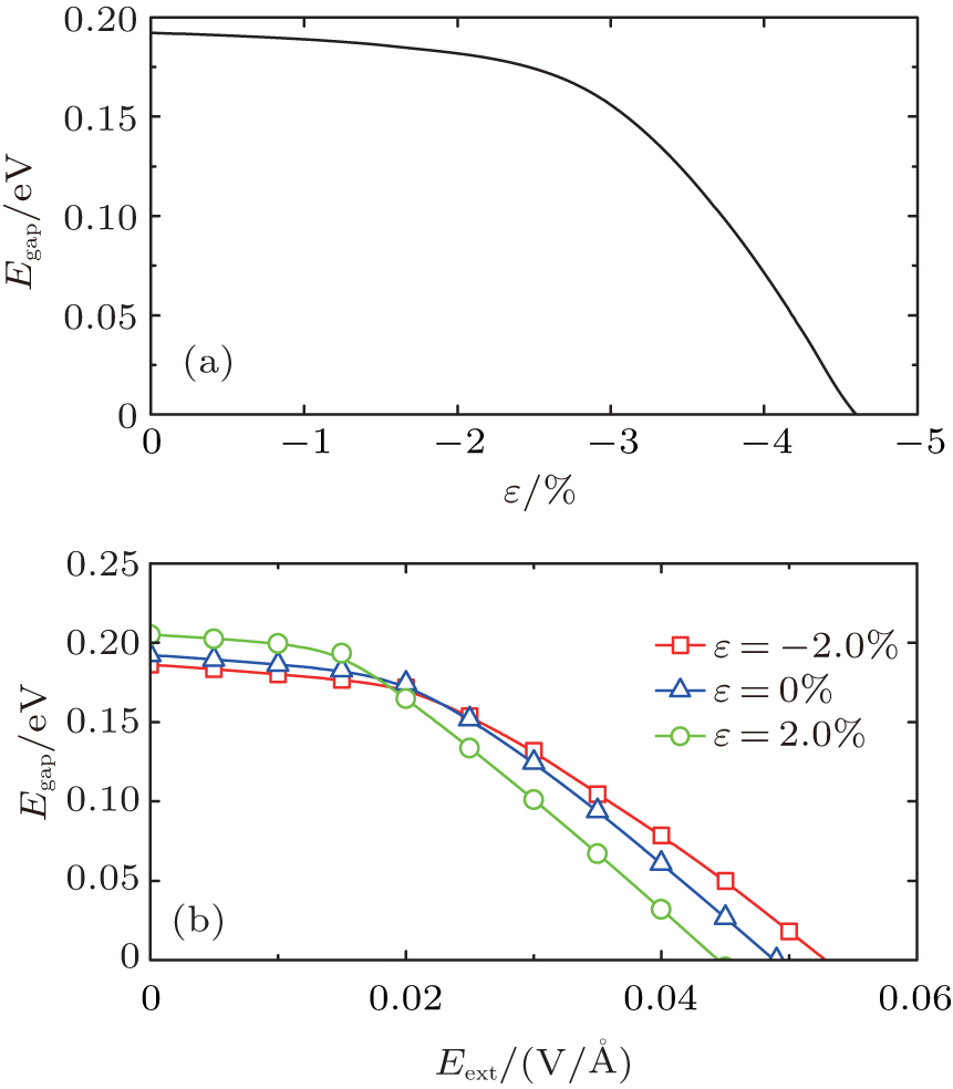 | Fig. 5. (a) Energy gap of T(5, 3) as a function of compressive strain. (b) Energy gap of T(5, 3) as a function of Eext under no strain, tensile, and compressive strain, respectively.[68] |
To understand this from another perspective, the band structure and partial charge densities of the lowest unoccupied crystal orbital (LUCO) and the highest occupied crystal orbital (HOCO) for T(5, 3) structure with the strain of ɛ = 4.0%, 0.0%, and -4.6% is depicted in Fig. 4, respectively. We can explain the role of the strain for the electronic properties from the effect of the Wilson transition. The compressive strain makes the interatomic distance decrease, then the hopping integral increase, which causes non-localization of orbits, and results in broadening bands, narrowed energy gap, even appearing zero gap. The tensile strain is opposite. From tensile strain to compressive strain, the densities of both the LUCO and HOCO increase slightly and become more non-localized. In particular, when the ɛ = − 4.6%, the (LUCO) and (HOCO) reaches at Γ point (k = 0) and the gap becomes zero.
Under the tensile (compressive) strain a weaker (stronger) electric field is needed to get zero gap, as shown in Fig. 5(b). From the partial charge density analysis, we conclude that under a weak tensile strain the charge of the V2 band near k = 0.25 and the C1 band near k = 0.5 become more sensitive to external transverse electric field than that without strain or with a weak compressive strain. Also a small tensile deformation makes the CSiNRs sensitive to electric field. Thus, a small tensile strain makes the SSiNRs more sensitive to external electric field. In addition, the strain induced or strain and electric field together modulated gapless spin-semiconducting property is also discovered in sawtooth graphene nanoribbons. This implies another perspective to modify electronic structures for applications in spintronics based on graphene or silicene.[68]
The magnetic properties of the silicene doped with Fe and Cr metal atoms under external electric field are investigated by the first-principles calculations. The low concentrations of metal atoms Fe or Cr substituting an Si atom in silicene produces two different structures denoted as X-I and X-II (X is Fe or Cr), as is shown in Fig. 6. The magnetic moments of Fe-I and Fe-II are 0 μ B and 0.45 μ B and the corresponding values are 2 μ B and 2.25 μ B for Cr-I and Cr-II, respectively.[18]
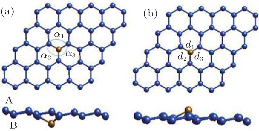 | Fig. 6. Two structures of Fe-doped silicene in the 4× 4 supercell. (a) Fe atom is below Si plane, labeled as Fe-I. (b) Fe atom is above Si plane, labled as Fe-II. α i and di are the bond angles and bond lengths, respectively.[18] |
Under a perpendicular field along the positive position shown in the inset of Fig. 7, there is an obvious ME effect for Fe-I and Fe-II with the corresponding ME coefficients of − 2.7× 10− 14 Gs· cm2/V and 0.22× 10− 14 Gs· cm2/V (1 Gs = 10− 4 T). But it is opposite for Cr-I and Cr-II. The ME coefficent (α s) is defined by μ 0Δ M = α sE to describe the ME properties in the linear region, where μ 0 is the vacuum magnetic permeability.[75– 77] Qualitatively, when the Eext changes from − 1 V/Å to 1 V/Å , the magnetic moment almost increases linearly for Cr-I, and the value of Cr-II firstly decreases linearly until Eext = 0, and then keeps a constant of 2 μ B, as shown in Fig. 7(b). The variation of the magnetic moment with the change of Eext in Fe-I (Fe-II) is as similar as that in Cr-I (Cr-II). Interestingly, there exists an abrupt jump of the magnetic moment when Eext is about − 0.65 V/Å for Fe-II and Eext is about − 0 V/Å for Fe-I, as depicted in Fig. 7(a). This ME behavior may have a potential application in ME devices demanding for the high speed response.
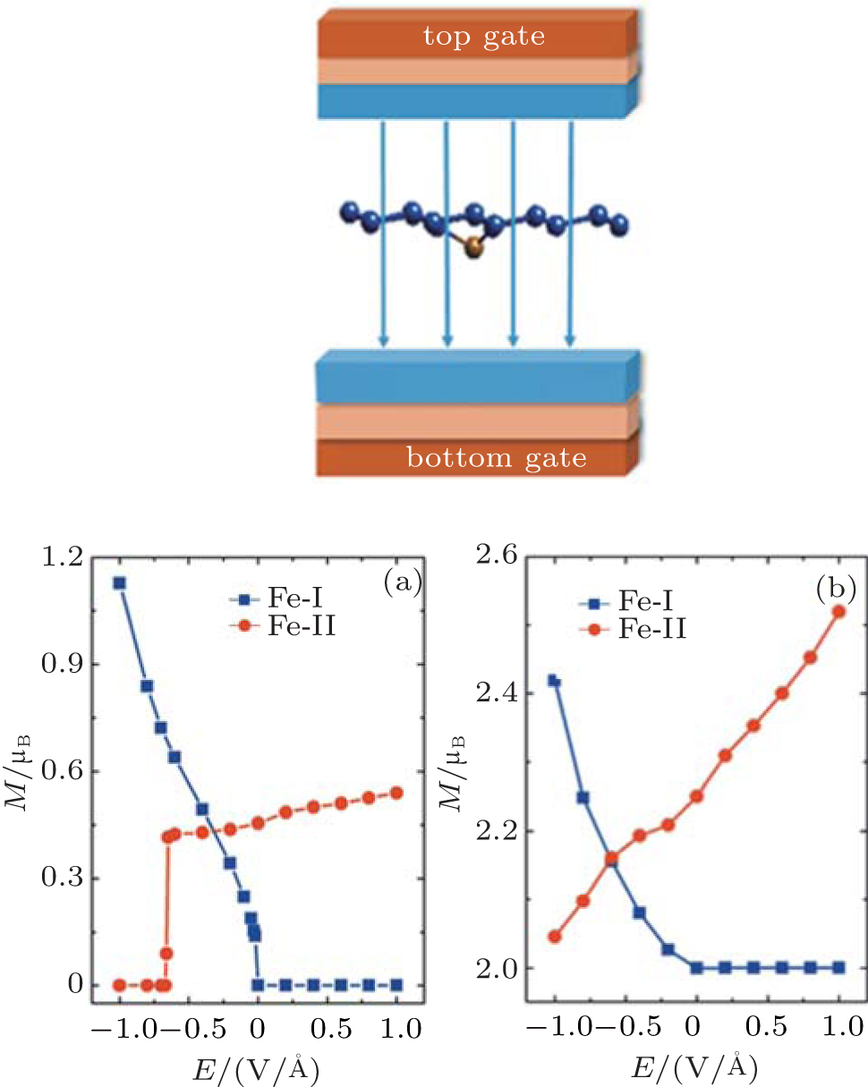 | Fig. 7. The magnetic moment of Fe- and Cr-doped silicenes for the 4× 4 supercell as a function of the external electric field. (a) Fe-I and Fe-II. (b) Cr-I and Cr-II. The left insert shows the direction of the electric field.[18] |
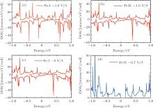
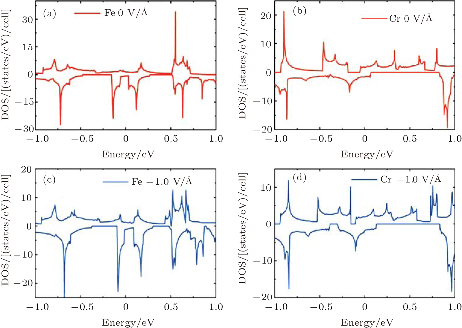
To gain a deep insight to the ME effects, the densities of states (DOS) are calculated. The ME effects are related to the electronic states around the Fermi level. When the Eext is 0 V/Å , there are no states of Fe-I across the Fermi level, as is shown in Fig. 8(a). With decreased electric field, the occupied spin-up states of Fe-I around the Fermi level become more and more, and at the same time, the corresponding spin-down states move above the Fermi level, which leads to the
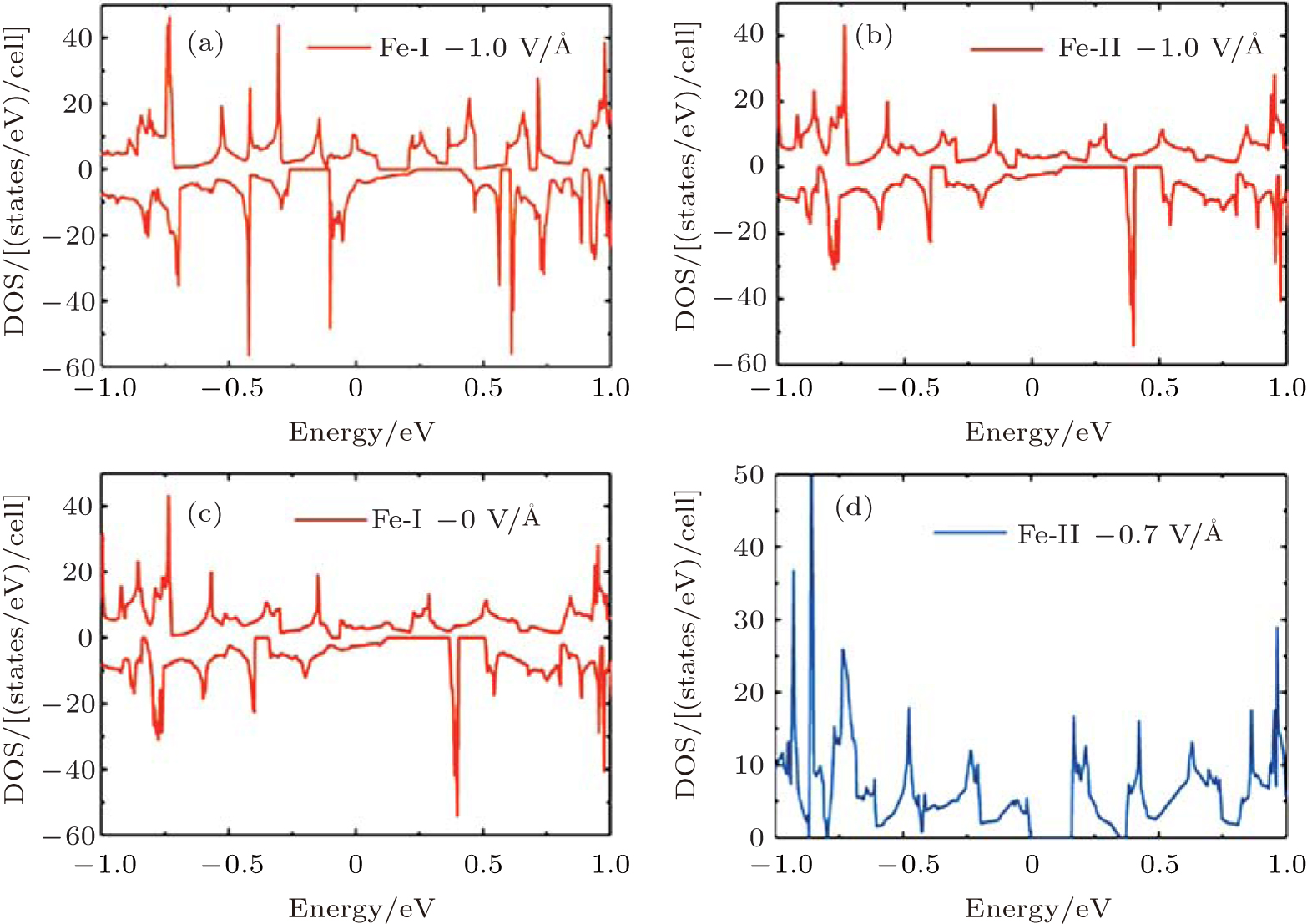 | Fig. 8. The densities of states (DOS) for the 4× 4 supercell under different electric fields. (a) The DOS of Fe-I with electric field of − 1.0 V/Å and 0 V/Å . (b) The DOS of Fe-II with electric field of 0 V/Å and − 0.7 V/Å .[18] |
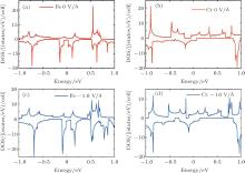
total magnetic moment accordingly increases. In contrast to Fe-I, the magnetic moment of Fe-II increases from − 0.65 V/Å to 1 V/Å . Figure 8(b) shows that there is less occupied states around the Fermi level when the electric field changes from 0 V/Å to − 0.7 V/Å . Especially around the − 0.7 V/Å , there is no spin polarization, which leads to 0 μ B. Compared to the case in the Fe doped-I system, more spin-up states of Cr-I are occupied around the Fermi level with the decreased electric field, but the corresponding spin-down states show little change with the variation of electric field, which contributes to larger magnetic moment than that in Fe-I system. For Cr-II, less states are occupied around the Fermi level with decreased electric field which results to small magnetic moment as shown in Fig. 9(b). Figure 10 shows the DOS of Fe- and Cr-doped silicenes in the 2× 2 supercell without the external electric field, indicating the existence of the magnetic moment.
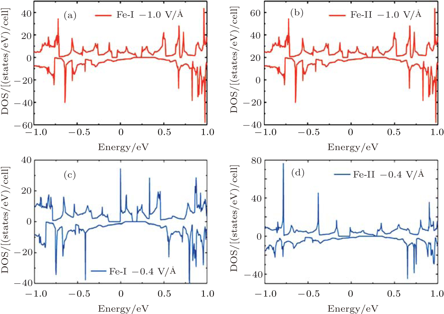 | Fig. 9. The DOS of (a) Cr-I and (b) Cr-II with electric field of − 1.0 V/Å and − 0.4 V/Å for the 4× 4 supercell.[18] |
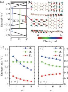
Two different ASiNRs can form an ASiSL. The ASiSL (n1, n2; s1, s2) is constructed of the segments ASiNR (n1) and ASiNR (n2), where s1 and s2 specify the length of segments in terms of the number of unit cell. Three families of ASiSLs under the combination of ASiNR (5), ASiNR (7), and ASiNR (9) are considered. The length of segments in ASiSLs can modulate the electron structure. The change of the electronic properties can be induced by the width of the superlattice, especially about some local electron and hole states.[78]
The size of superlattices has an important impact on the electronic structure and properties of ASiSLs. The band structure of the ASiSL (5, 7; 3, 3) is shown in Fig. 11(a). While the highest (lowest) valance (conduction) band is dispersive, the second valance and conduction bands are flat which are verified as confined states. The confined states do not appear singly in the constituent ribbons of the superlattice. Figure 11(b) presents that although the first dispersive state propagates across the whole superlattice, the distribution of the Bloch function for dispersive state located mostly at the narrow part, and the first confined state mainly located at the wider part. Figure 11(c) illustrates that the band gap and relative energy gaps in ASiSL (5, 7; s1, s2) are varied with the length of the narrower or wider nanoribbons. For s2 = 3, as s1 increases, the band gap Eg and the energy gap Δ 2 decrease but the energy gap of the confined states, Δ 1, has no interest of s1. However, as can be seen in Fig. 11(d), the band gap Eg goes up with the increase of s2 when s1 is fixed and at the same time, the energy gaps Δ 1 and Δ 2 decrease when the wider nanoribbon becomes longer.
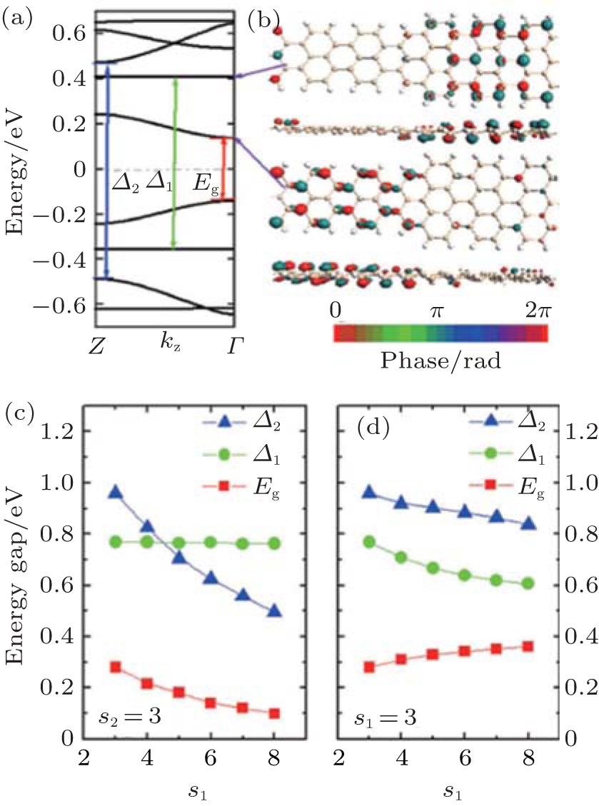 | Fig. 11. (a) The band structure of ASiSL (5, 7; 3, 3) with flat bands corresponding to confined states. Here Eg is the band gap of the superlattice; Δ 1 is the energy gap of the highest localized state while Δ 2 is the energy gap for the next dispersive state. (b) The Bloch states of the first dispersive and confined state at the Γ point of the Brillouin zone. (c) The variation of the energy gaps of the ASiSL (5, 7; s1, 3) from s1 = 3 to 8. (d) The variation of the energy gaps of the ASiSL (5, 7; 3, s2) from s2 = 3 to 8.[78] |
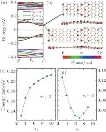
Different from the the ASiSL (5, 7; 3, 3), the highest valence and lowest conduction bands of the ASiSL (5, 9; 3, 3) are the confined states, and yet the second conduction and valence bands behave as the dispersive states, as presented in Fig. 12(a). The shape of the ASiSL (5, 9; 3, 3) is a saddle and the Bloch state of the confined state primarily distributes at the interface between the wide and narrow segments, but the dispersive state cannot propagate across the whole superlattice, just locatting at its narrower part, showed by Fig. 12(b). The interface between two different nanoribbons and the shape of the superlattices may affect its electronic properties. The effect of the narrower and wider segments on the electronic structure of ASiSL (5, 9; s1, s2) is shown in Figs. 12(c) and 12(d). The behavior of the energy gaps Δ 1 and Δ 2 in the bands of ASiSL (5, 9; s1, 3) is the same as that of ASiSL (5, 7; s1, 3) with the increase of s1. The gaps of ASiSL (5, 9; s1, 3) are of particular interest with s1 changed. When s1 ≤ 5, the band gap Eg is equal to Δ 1; but for s1 ≥ 6, the subsequent gap is related to Δ 2 because the band structure of the superlattice is tuned. Figure 12(d) shows that when s1 is fixed, the band gap (Eg = Δ 1) always drops with the increase of s2, but Δ 2 keeps stable for s2 ≥ 5.
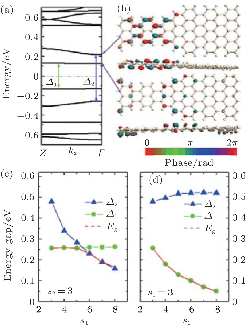 | Fig. 12. (a) The band structure of ASiSL (5, 9; 3, 3) with flat bands corresponding to confined states (Eg = Δ 1). (b) The Bloch states of the first dispersive and confined state at the Γ point of the Brillouin zone. (c) The variation of the energy gaps of the ASiSL (5, 9; s1, 3) from s1 = 3 to 8. (d) The variation of the energy gaps of the ASiSL (5, 9; 3, s2) from s2 = 3 to 8.[78] |
The band structures of ASiSL (7, 9; s1, s2) are quite different from that of ASiSL (5, 7; s1, s2) and (5, 9; s1, s2), presented in Fig. 13. For example, there is no plat states in the ASiSL (7, 9; 3, 3) and the edge states are dispersive with an energy gap of 0.13 eV in Fig. 13(a). As one can see from Fig. 13(c), the band gap of the ASiSL (7, 9; s1, 3) firstly rises sharply, then it changes slowly with the increase of s1. But the variation of the band gap with the increase of s2 is significantly different in Fig. 13(d). The band gap drops down until s2 = 7, and then it goes up fastly, which means there exists a valley. Figure 13(b) shows the Bloch states of the edge state of ASiSL (7, 9; 3, 3) and ASiSL (7, 9; 5, 3) at the Γ point of the Brillouin zone.
 | Fig. 13. (a) The band structure of ASiSL (7, 9; s1, 3) with increasing s1 from 3 to 10. (b) The Bloch states of the edge state of ASiSL (7, 9; 3, 3) and ASiSL (7, 9; 5, 3) at the Γ point of the Brillouin zone are displayed, respectively. (c) The variation of the band gaps of the ASiSL (7, 9; s1, 3) from s1 = 3 to 10. (d) The variation of the gaps of the ASiSL (7, 9; 3, s2) from s2 = 3 to 9.[78] |
The band structures and Bloch states of the ASiSL (11, 9; 3, 3) and (11, 13; 3, 3) in Fig. 14(a) are similar to that of the ASiSL (7, 9; 5, 3) and (5, 7; 3, 3). The condition Δ n = n1 − n2 = 2 is also satisfied. One can find that the edge states of the band structure in the superlattice are the dispersive or confined states, the confined states are localized mainly at the wider parts, the dispersive states propagate across the ASiSL and the distribution of the Bloch states is rare at the wider parts. In view of the band gap of constituent nanoribbons, the edge states of these superlattices mainly distribute in the parts which have the lower energy gap.
The different superlattices which satisfy Δ n = 4 are constructed, presented in Fig. 14(b). The electronic structures of the ASiSLs (11, 7; 3, 3) and (11, 15; 3, 3) have the similar results as that of the ASiSL (5, 9; 3, 3). The dispersive (confined) state mainly locates at the narrower segments (the wider parts and/or interfaces). In addition, figure 14(c) gives the electronic structure and properties of the ASiSL (5, 11; 5, 3) and (7, 13; 5, 3) when Δ n = n1 − n2 = 6. Then the two constituent armchair ribbons of the ASiSL have the same band gap type but the wider part has smaller gap. There is one dispersive and two plat states in conduction and valence bands near Fermi level, respectively. The first confined state only locates at the interface of the superlattice; the first dispersive and second confined states may distribute at either the narrower or wider parts. The quantum phenomena mentioned above may be related to the interface effect because the interface with incomplete hexagons differs from the adjacent nanoribbons at different sides of the superlattice. The edge states of these superlattices with larger width difference do not necessarily distribute in the parts with smaller gap.
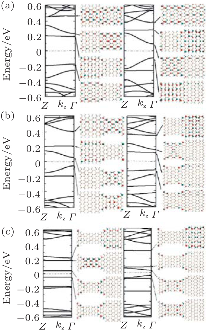 | Fig. 14. Band structures and Bloch states for several superlattice structures. (a) ASiSL (11, 9; 3, 3) and ASiSL (11, 13; 3, 3). (b) ASiSL (11, 7; 3, 3) and ASiSL (11, 15; 3, 3). (c) ASiSL (5, 11; 5, 3) and ASiSL (7, 13; 5, 3).[78] |
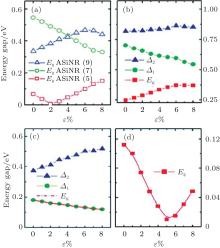
The role of the tensile strain for the the electronic structures of the nanoribbons and superlattices are also investgated. The three different types of the band gaps of ASiNR (5), ASiNR (7), and ASiNR (9) during strain are illustrated in Fig. 15(a). The strain was applied to these superlattices along axial direction, and allowed to relax for the other two directions. The strain is defined as ɛ = (L − L0)/L, where L0 and L are the equilibrium lengths along the axial direction for the unit cell of the unstrained and strained superlattices, respectively. For ASiNR (5), with increasing the strain ɛ the band gap firstly decreases until ɛ = 2 %, and then increases gradually; On the contrary, the band gap of ASiNR (9) goes up at
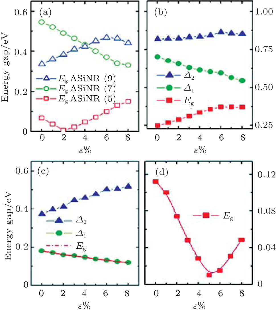 | Fig. 15. Variation of band gaps and related energy gaps in the ASiSL and the constituent nanoribbons with respect to strain ɛ . (a) ASiNR (5), ASiNR (7), and ASiNR (9). (b) ASiSL (5, 7; 4, 4). (c) ASiSL (5, 9; 4, 4). (d) ASiSL (7, 9; 4, 4).[78] |
the beginning, but reduces when ɛ is more than 6 %; the gap of ASiNR (7) always drops down when ɛ changes from 0 to 8 %. The variations of band gaps and other relevant energy gaps (Δ 1, Δ 2) in all three ASiSLs mentioned above with respect to the strain ɛ are presented in Figs. 15(b)– 15(d), respectively. For the ASiSL (5, 7; 4, 4), with increasing the strain ɛ the band gap Eg always increases but the energy gap between two confined states (Δ 1) sharply decreases while Δ 2 almost has no change. The band gap Eg and energy gap Δ 1 of ASiSL (5, 9; 4, 4) become smaller and smaller as ɛ increases gradually, which is opposite of that of Δ 2. In ASiSL (7, 9; 4, 4), the band gap Eg varies like a valley following the increase of ɛ and reaches the minimum when ɛ is about 5 %. Under different strains, the electronic properties of ASiSLs are various. However, it has nothing to do with the behavior of the constituent ribbons by a lot of analysis.[78]
In summary, we reviewed our recent works about the structural, energetic, and electronic properties of two types of sawtooth silicene nanoribbons and the various types of ASiSLs, and the structure and ME of the silicene doped with Fe or Cr atoms. Based on the DFT calculations, we found that due to the edge stats, the SSiNRs are spin-semiconductors with the ferromagnetic ground state. Moreover, by the study of the charge distributions of the edge states in real space, the SSiNRs turn into the spin gapless semiconductor under a lower external electric field or suitable compressive strain. The systems of the silicene doped with Fe and Cr atoms, applying the external electric field, show a variety of interesting ME behaviors: (i) The magnetic moment of Fe-doped silicene shows a sharp jump at a threshold electric field, which indicates a good switching effect; (ii) For the low concentrations of Fe- or Cr-doped silicenes, there are two structures in which the changes of magnetism are significantly different under external electric field and the changes of magnetic moment strongly depend on the direction of the electric field; (iii) The magnetic moment of the doped systems has a nearly linear region with the electric field. In addition, the electric and structures properties of ASiSLs are modulated by the size and length of the narrow and wide nanoribbons, as well as the strain of superlattices, which also play interest roles in the distribution of the localized and dispersive states of superlattices. When the stain increases, the related energy gaps of ASiSLs will change, which are significantly different with that of the constituent nanoribbons. All these results lay a deeply foundation for the practical applications for the spintronics and nanodevices.
| 1 |
|
| 2 |
|
| 3 |
|
| 4 |
|
| 5 |
|
| 6 |
|
| 7 |
|
| 8 |
|
| 9 |
|
| 10 |
|
| 11 |
|
| 12 |
|
| 13 |
|
| 14 |
|
| 15 |
|
| 16 |
|
| 17 |
|
| 18 |
|
| 19 |
|
| 20 |
|
| 21 |
|
| 22 |
|
| 23 |
|
| 24 |
|
| 25 |
|
| 26 |
|
| 27 |
|
| 28 |
|
| 29 |
|
| 30 |
|
| 31 |
|
| 32 |
|
| 33 |
|
| 34 |
|
| 35 |
|
| 36 |
|
| 37 |
|
| 38 |
|
| 39 |
|
| 40 |
|
| 41 |
|
| 42 |
|
| 43 |
|
| 44 |
|
| 45 |
|
| 46 |
|
| 47 |
|
| 48 |
|
| 49 |
|
| 50 |
|
| 51 |
|
| 52 |
|
| 53 |
|
| 54 |
|
| 55 |
|
| 56 |
|
| 57 |
|
| 58 |
|
| 59 |
|
| 60 |
|
| 61 |
|
| 62 |
|
| 63 |
|
| 64 |
|
| 65 |
|
| 66 |
|
| 67 |
|
| 68 |
|
| 69 |
|
| 70 |
|
| 71 |
|
| 72 |
|
| 73 |
|
| 74 |
|
| 75 |
|
| 76 |
|
| 77 |
|
| 78 |
|