Silicene spintronics — A concise review
Wang Yang-Yanga), c) † , Quhe Ru-Gea), d), e), f) † , Yu Da-Penga), b) , Lü Jing‡a), b) 
Silicene spintronics — A concise review |
|
Wang Yang-Yang
|
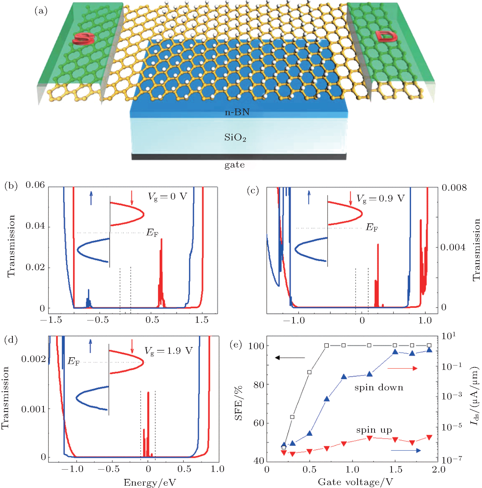
| (a) Schematic diagram of two-probe model of H@silicene sheet spin-filter device with SiO2 dielectric and h-BN buffer layer. (b)–(d) The spin-polarized transmission spectra with V g = 0, 0.9, and 1.9 V, respectively. The bias voltage is fixed at V bias = 0.2 V. Red (blue) line stands for the spin down (up). The vertical dashed lines denote the bias voltage window. Insets are the schematic plot of the Fermi level shift with the gate voltage. (e) Spin-filter efficiency and spin-resolved current as a function of the gate voltage. Reproduced with permission from Ref. [ 37 ]. Copyright 2013 Elsevier B.V. |
| |