


Silicene spintronics — A concise review*
[Wang Yang-Yanga), c) † , Quhe Ru-Gea), d), e), f) † , Yu Da-Penga), b) , Lü Jing‡a), b)  ]
]
]
|
|


†These authors contributed equally to this work.
‡Corresponding author. E-mail: jinglu@pku.edu.cn
*Project supported by the National Natural Science Foundation of China (Grant Nos. 11274016 and 11474012), the National Basic Research Program of China (Grant Nos. 2013CB932604 and 2012CB619304), and a National Science Foundation (Grant No. 1207141).
Spintronics involves the study of active control and manipulation of spin degrees of freedom in solid-state systems. The fascinating spin-resolved properties of graphene motivate numerous researchers to study spintronics in graphene and other two-dimensional (2D) materials. Silicene, the silicon analog of graphene, is considered to be a promising material for spintronics. Here, we present a review of theoretical advances with regard to spin-dependent properties, including the electric field- and exchange field-tunable topological properties of silicene and the corresponding spintronic device simulations.
Spintronics, or spin electronics, aims to exploit spin degrees of freedom instead of or in addition to charge degrees of freedom for information storage and logic devices. Compared with conventional semiconductor devices, spintronic devices have the potential advantages of nonvolatility, increased data processing speed, decreased electric power consumption, and increased integration densities. Currently, the major challenge of spintronics is the difficulty in generating, controlling and detecting spin-polarized current. Graphene, with a high electronic mobility of 2.× 105 cm2/(V· s)[1, 2] and a long spin diffusion length of several micrometers[3– 5] is quite attractive for application in spintronics. Since its first isolation in 2004, a variety of graphene-based spintronic devices have been proposed, [6, 7] such as spin valves, [8] large-magnetoresistance (MR) devices, [9] and graphene nanoribbon (GNR)-based giant MR devices, spin-filters, and spin transistors.[10– 14]
Silicene, the silicon counterpart of graphene, is predicted to be another Dirac material and has recently been successfully fabricated via epitaxial growth on Ag (111), [15– 19] ZrB2 (0001), [20] Ir (111), [21] and MoS2[22] surfaces. A silicene field-effect transistor (FET) operating at room temperature was fabricated very recently, [23] corroborating theoretical expectations regarding its ambipolar Dirac charge transport. Compared with graphene, silicene has a longer spin-diffusion time (τ s = 1 ns at 85 K and 500 ns at 60 K versus τ s = 0.1 ns at 300 K), a longer spin coherence length (ls = 10, 350, 2000 μ m versus ls= 1.5 μ m and 2 μ m at room temperature), and a much larger spin– orbit coupling (SOC) gap (1.55 meV versus 10− 3 meV).[3, 24– 29] Therefore, silicene appears more suitable for spintronic applications and could fit into industrial silicon-based circuits more easily than graphene.
In spintronics, half-metallic materials, with a metallic nature for one spin and an insulating or semiconducting nature for the other spin, are highly desired because they could provide 100% spin polarized current. Due to their peculiar edge states, zigzag silicene nanoribbons (ZSiNRs) provide a good platform for the realization of half-metallicity by transverse electric field[30] and asymmetric edge modification.[31– 34] Spin-filters and spin FETs are designed based on the half-metallicity in ZSiNRs. Moreover, a giant MR can be obtained in ZSiNRs either by utilizing a switchover between different magnetic states[35] or symmetry-dependent transport property.[36] Half-metallicity can also be achieved in semihydrogenated silicene by applying an out of plane gate voltage. By adjusting an electric field and/or an exchange field, quantum spin Hall effects (QSHE), quantum anomalous Hall effects (QAHE), valley-polarized QAHE, and quantum valley Hall effects (QVHE) can be expected in pristine silicene, potentially enabling many applications for spintronic devices. This review is organized into the following main parts: spintronics in zigzag silicene nanoribbons (Section 2); spintronics in semihydrogenated functionalized silicene (Section 3); tunable quantum topological states in silicene and corresponding spintronic applications (Section 4). Conclusion and outlook are given in Section 5.
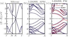
ZSiNRs have drawn a lot of attention due to their remarkable application potential in spintronics. The ground state of ZSiNRs has the two edges antiferromagnetically coupled, which is slightly lower in energy than the ferromagnetic (FM) state as a result of edge magnetic states coupling.[30] Due to the spin degeneracy of the antiferromagnetic (AFM) state, spin-polarized transport cannot be realized in pristine ZSiNRs (Fig. 1). Therefore, various approaches were utilized to break the spin degeneracy in ZSiNRs, such as applying external electric field[30] and edge modification, [31– 34] just like in the zigzag GNRs.[11, 14]
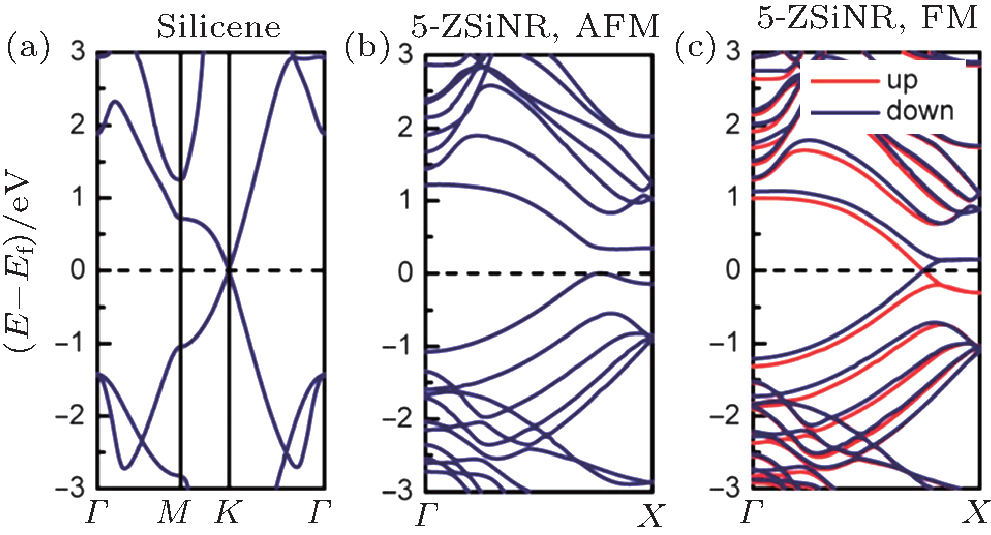 | Fig. 1. Band structures of (a) silicene, (b) the AFM 5-ZSiNR, and (c) the FM 5-ZSiNR. Reproduced with permission from Ref. [35]. Copyright 2012 Royal Society of Chemistry. |
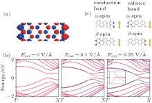
The half-metallicity could be induced by an in-plane homogenous electric field in the hydrogen-terminated ZSiNRs.[30] The zero-field α -spin and β -spin orbitals in the conduction and valence bands are localized at the opposite edges of the nanoribbon, and in a given edge, the spin orientations in the conduction and valence bands are opposite (Fig. 2(c)). As the transverse electric field Eext increases, the spin degeneracy of the conduction and valence bands is lifted. The band gap of the β -spin state decreases and finally closes under Eext = 0.25 V/Å , while that of the α -spin state increases slightly relative to the zero-field value. Therefore, the transverse electric field-induced half-metallicity in ZSiNRs is well established (Fig. 2(b)).
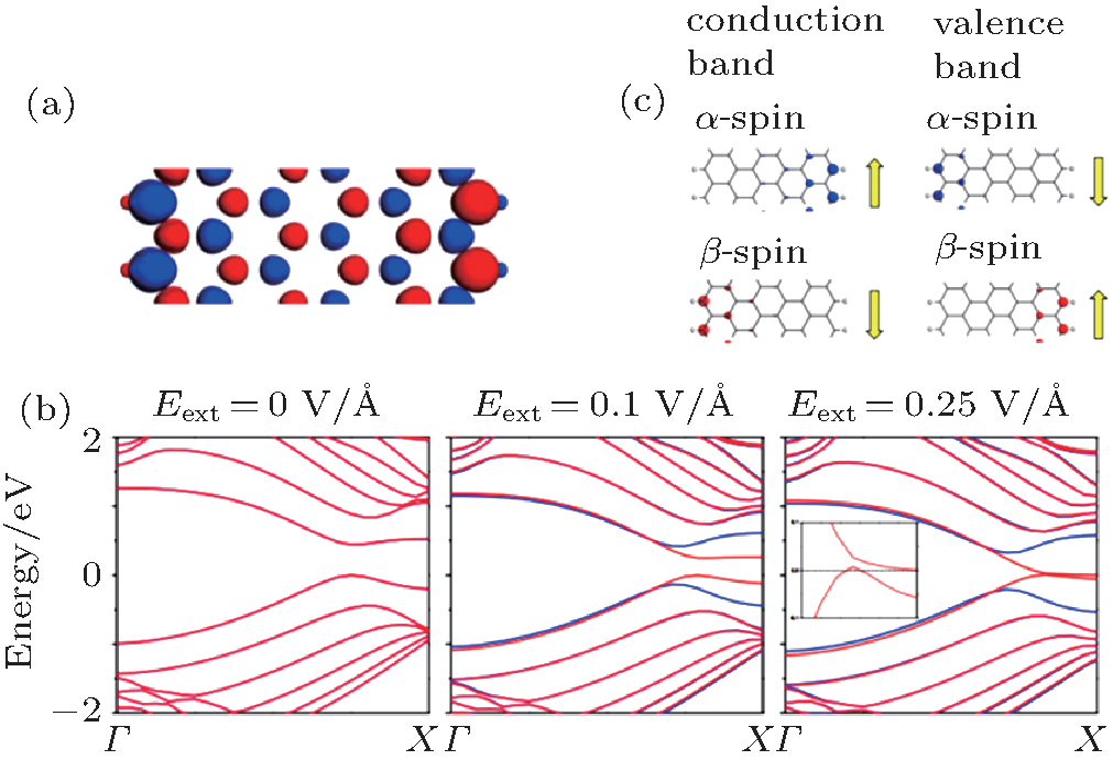 | Fig. 2. Electronic properties of 6-ZSiNR in the ground state. (a) Spatial spin density distribution. The isovalue is 0.006 a.u. (b) Spin-resolved band structures under Eext= 0, 0.1, and 0.25 V/Å , respectively. Inset: the band structure with Eext = 0.25 V/Å in the range of | E| < 0.1 eV and 0.7π /a ≤ k ≤ π /a (the horizontal line is Ef. The valence top or Ef is set to zero. (c) The α -spin and β -spin orbitals of the conduction and valence bands, shown as the square of the absolute value of the wavefunction summed over all k-points. The isovalue is 0.275 a.u. The yellow arrow represents the energy shift direction of the spin states under a transverse electrical field. Blue and red denote α -spin and β -spin, respectively. Reproduced with permission from Ref. [30]. Copyright 2012 World Scientific Publishing Company. |
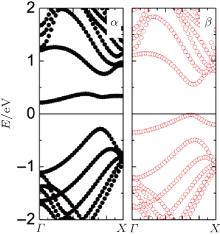
Asymmetric edge modification is another way to transform ZSiNRs to half-metals.[31– 34] One of these interesting methods is asymmetric edge hydrogenation (H2– ZSiNR– H).[31, 33, 34] Several theoretical works have demonstrated that the ground state of H2– ZSiNR– H is an FM semiconductor. Around the Fermi level (Ef, the states are completely spin-polarized with opposite spin orientations, defining a bipolar magnetic feature in the asymmetric ZSiNRs (Fig. 3).[31] This special distribution will bring interesting magnetic behaviors for doped H2– ZSiNR– H. In doped systems, Ef will shift into the valence or conduction band, and H2– ZSiNR– H becomes a half metal.
 | Fig. 3. The spin-polarized band structures for the asymmetric 6-ZSiNRs. Reproduced with permission from Ref. [31]. Copyright 2013 American Physical Society. |
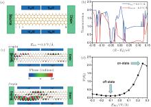
A ZSiNR spin-filter under a transverse electrical field is illustrated in Fig. 4(a).[30] Transportation properties are simulated by using density functional theory (DFT) coupled with the nonequilibrium Green’ s function (NEGF) formalism. In the spin-resolved transmission spectrum of this device under Egate = 0.3 V/Å , there is a large peak for the α -spin around Ef and a clear gap for the β -spin (Fig. 4(b)). Consistently, the spin-resolved transmission eigenstates at Ef and the Γ point in k-space in Fig. 4(c) also reflect this high spin polarization. The spin-filter efficiency, defined as SFE = (Iα − Iβ )/(Iα + Iβ ), where Iα and Iβ represent the α -spin and β -spin current densities, respectively. The changes of T(Ef) and SFE as a function of Egate are shown in Fig. 4(d). The T(Ef) values for the two spins are symmetric about Egate = 0. Even at small Egate = − 0.05 V/Å or 0.05 V/Å , the T(Ef) between the two spins has a difference with SFE = 62.3%. The difference becomes more and more significant with the increasing Egate, a behavior consistent with the electrical field-induced change in the band gap of ZSiNRs. SFE is nearly saturated (99%) from | Egate| > 0.2 V/Å . Therefore, the dual-gated finite ZSiNR can serve as a nearly perfect spin-filter, with sign switchable by altering the electric field direction. Similarly, a perfect spin filtering effect can be expected in a doped half metal H2– ZSiNR– H. The study shows that an SFE of 100% is achieved with the unchanged spin states in a very large bias region from − 0.5 V to 0.5 V without the magnetic field being applied (Fig. 5).[34]
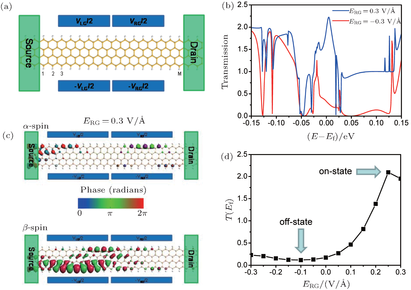 | Fig. 4. Spin-filter based on the 4-ZSiNR. (a) Schematic model with one pair of gate electrodes on the two sides. (b) Spin-resolved transport spectrum under Egate = 0.3 V/Å . (c) Spin-resolved transmission eigenstate at Ef and the Γ point in k-space under Egate = 0.3 V/Å . The isovalue is 1.0 a.u. (d) Spin-resolved transmission coefficient at Efk-space and spin filtration efficiency as a function of Egate. Reproduced with permission from Ref. [30]. Copyright 2012 World Scientific Publishing Company. |
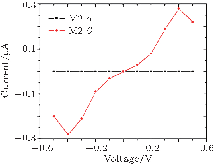 | Fig. 5. I − V curves for the α -spin and the β -spin states at various biases. Reproduced with permission from Ref. [34]. Copyright 2013 Nature Publishing Group. |
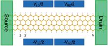
Besides the proposed spin-filter, ZSiNR may also serve as the channel of an effective spin FET with quadruple-gate, as illustrated in Fig. 6.[30] The electrical field of the left pair of electrodes (ELG) is fixed and the on– off switch is achieved by modulating the right one (ERG). When ERG = ELG, the left and right parts of the nanoribbon allow the same spin to transport along the edges. This device degenerates into a spin-filter with Egate = ERG = ELG. When the direction of the electrical field of the right pair of electrodes is reversed, the sign of the allowed traveling spin in the right part of the nanoribbon is reversed and opposite to that in the left part, resulting in a possible blockade of the transmission of both spins. As a result, the current of this device is expected to be forbidden in this case. Therefore, through altering ERG and thus altering the spin state, the quadruple-gated device can operate as a spin FET. The maximal on/off conductance ratio of the present device is 18. The low on/off ratio is ascribed to the quiet short channel (38.3 Å ) controlled by each pair of electrodes in this simulation limited by the computational resources, which gives rise to a certain amount of leakage current on the off-state due to tunneling effect. If the channel length were to be increased, a higher on/off ratio is expected because the leakage of both spin currents will be reduced.
 | Fig. 6. Schematic model of the quadruple-gated spin FET based on the 4-ZSiNR. Reproduced with permission from Ref. [30]. Copyright 2012 World Scientific Publishing Company. |
The AFM state of ZSiNRs is semiconducting, while the FM state is metallic. If a proper magnetic field is applied, ZSiNRs can switch between the AFM and the FM configurations (Figs. 7(a) and 7(b)), and consequently a large MR can be obtained because of a large current difference between the semiconducting AFM and the metallic FM configurations (Fig. 7(c)). Usually MR is calculated by the optimistic definition, which is MR(Vbias) = (IFM− IAFM)/IAFM, where Vbias is the applied bias voltage, IFM (IAFM) is the total current of the FM (AFM) configuration. As shown in Fig. 7(d), the MRs of different ZSiNRs at the same bias voltage drop generally with increasing ribbon width, except 4-ZSiNR. In the examined bias range from 0.05 V to 0.5 V, the maximum MRs of the ZSiNRs are 261%– 1960%.
The critical magnetic field B* required to switch a ZSiNR between the AFM and FM configurations can be estimated from the relation

where Δ is the energy difference between the AFM and FM configurations, g = 2 is the Landauer factor of silicene, μ B = 0.058 meV/T is the Bohr magneton, and MT is the total spin on edge atoms. The resulting B* of the 5-ZSiNR is 8.6 T, which is easily attainable in the laboratory.
Apart from applying a magnetic field, some peculiar symmetry-dependent transport properties of FM ZSiNRs can also be utilized to achieve a giant MR.[36] Due to the existence of a two-fold axis, the π and π * wavefunctions in even-N ZSiNRs have opposite parity with respect to the c2 operation. The transmission of electron from the π band of the left electrode to the π * band of the right electrode is forbidden, leading to a conductance gap near Ef. On the other hand, the transmission is allowed in odd-N ZSiNRs because the π and π * wavefunctions have no definite parity.
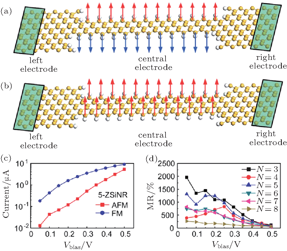 | Fig. 7. (a) and (b) Schematic models of an H-passivated ZSiNR connected to two semi-infinite silicene structures. (a) The 3-ZSiNR in the AFM configuration. (b) The 4-ZSiNR in the FM configuration. Applying or removing magnetic field adjusts the ferromagnetic coupling of the two edges. The yellow (gray) balls denote silicon (hydrogen) atoms. The arrows represent spin directions on the edges. (c) I– Vbias characteristics of the 5-ZSiNR at the AFM and FM configurations. (d) MRs of different-width ZSiNRs as functions of bias voltage. Reproduced with permission from Ref. [35]. Copyright 2012 Royal Society of Chemistry. |
Two spin configurations, P and AP, are considered in a two-probe system of even-N ZSiNRs (Figs. 8(b) and 8(c)). Both the left and right electrodes are spin-up polarized in the P configuration, while in the AP configuration the two electrodes have antiparallel spin polarization direction. Figure 8(d) shows the I– V relationship for different spin components. The magnitude of MR can be obtained according to the definition MR = (IP– IAP)/IAP, where IP and IAP are currents in P and AP configurations, respectively. The spin-up, spin-down, and total MRs are all on the order of 106% (Fig. 8(e)). The appearance of the MR effect can be understood by Figs. 8(f) and 8(g). For the P configuration (Fig. 8(f)), near Ef the spin-up π bands of the two electrodes overlap, as do the spin-down π * bands, so transmission is allowed. So near the Fermi level, the conductance is about 1 G0 for both spin components, and the current increases with increasing bias. The situation differs in the AP configuration. As shown in Fig. 8(g), near Ef the spin-up π * (spin-down π ) band of the left electrode only overlaps the spin-up π (spin-down π * ) band of the right electrode. As discussed above, the π and π * bands have opposite parity; thus transmission between them is forbidden. As a result, a conductance gap appears around Ef for both spin components, and the corresponding current is almost zero.
 | Fig. 8. (a) Band structure of FM 6-ZSiNR. The spin-up and spin-down components are presented in red and blue lines, respectively. (b) and (c) Spin density for 6-ZSiNR with P and AP configurations under zero bias. The two electrodes have parallel spin configuration in the P case but antiparallel spin configuration in the AP case. Pink and blue surfaces denote the spin-up and spin-down components, respectively. The isosurface corresponds to 0.01 e/Å 3. (d) I– V curves for the P and AP configurations. Inset is a semi-logarithmic scale plot. (e) Spin up, spin down, and total magnetoresistance on a semi-logarithmic scale. (f) and (g) Band structures for left and right electrodes, and transmission spectra for P (f) and AP (g) configurations under zero bias. Solid and open circles denote π and π * states. Solid arrows indicate allowed transmissions, and dashed arrows indicate forbidden transmissions. G0 equals e2/h. Reproduced with permission from Ref. [36]. Copyright 2012 American Institute of Physics. |
The semihydrogenated silicene (H@silicene) shown in Figs. 9(a) and 9(b) is dynamically stable, as demonstrated by molecular dynamics and phonon mode dispersion calculations.[37] According to DFT calculations, H@silicene is an FM semiconductor with a band gap of 0.93 eV (Fig. 9(c)), and both electronic and spintronic applications can be expected. Regarding the spin-polarized band structures, the Fermi level can be shifted into the valence or conduction bands by applying an out-of-plane gate voltage. Therefore half metal behavior can be expected in H@silicene.
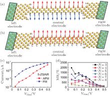
A single-gated H@silicene device, shown in Fig. 10(a), was simulated by the DFT-NEGF method. As discussed above, by changing the gate voltage to shift Ef into the valence or conduction band, a half metal behavior can be expected in the H@silicene device. Therefore, spin-filters and spin switches can be achieved. As shown in Fig. 10(b), when Vg = 0 V, the transmission probability nearly vanishes, responsible for the off-state for spin up and spin down. Ef shifts upward as Vg increases (Fig. 10(c)). When Vg = 1.9 V (Fig. 10(d)), Ef is located in the middle of a subband of spin down, and an effective on-state for spin down is achieved. With an increase of gate voltage, the current density of the spin-down increases significantly, but that of the spin-up increases slightly, as shown in Fig. 10(e). As a result, the SFE increases with increasing gate voltage and reaches 100% at Vg = 1.9 V.
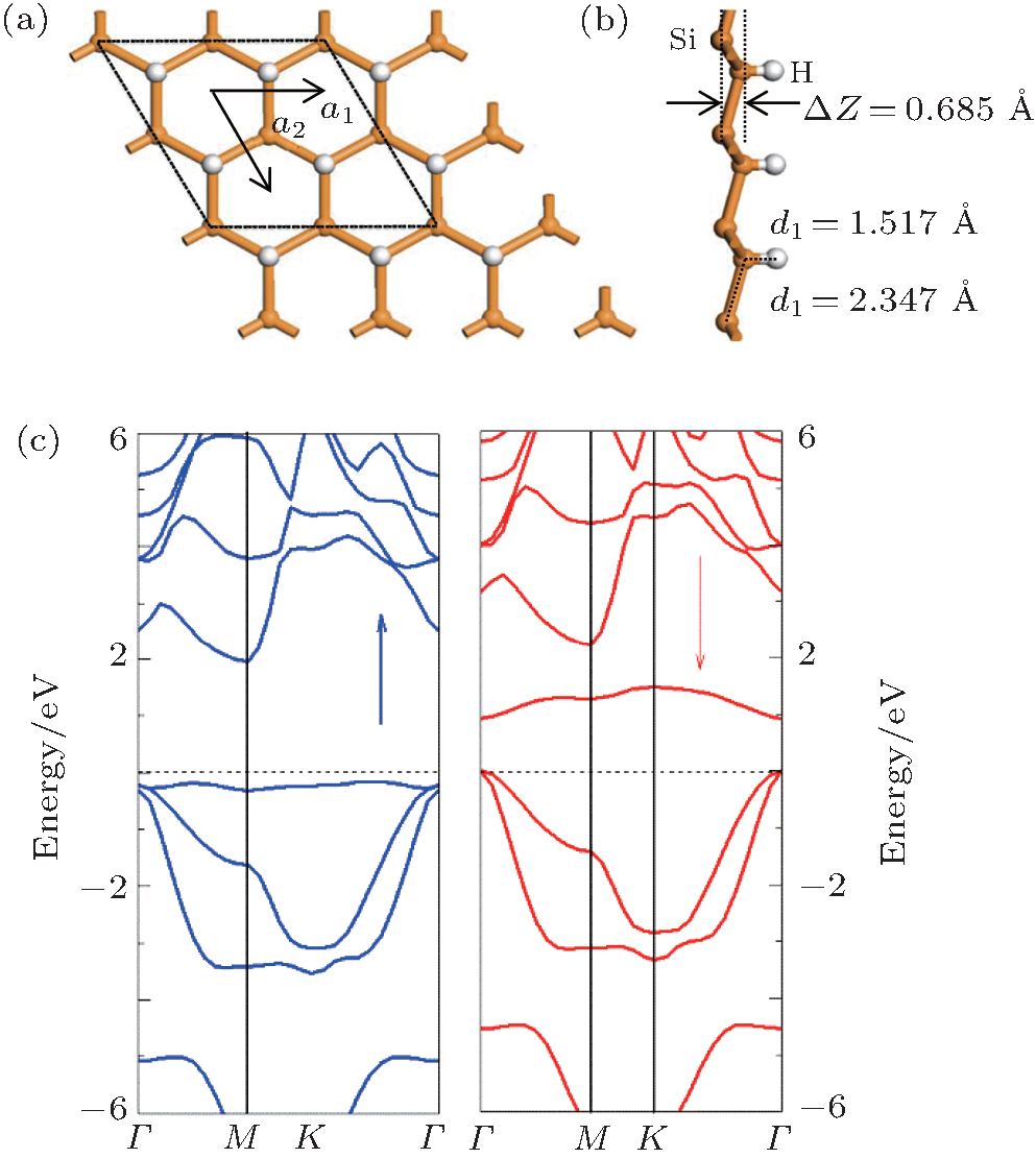 | Fig. 9. Optimized geometric atomic configurations and structural parameters of H@silicene. (a) Top view with the rhombus marked in black showing the supercell. Bravais lattice vectors of a unit cell are given with a1 = a2 = a = 3.899 Å . (b) Side view. The average bond length d1 (Å ) between Si and H atoms, d2 (Å ) between Si and Si atoms, and buckled height Δ Z(Å ) between Si and Si layers. The yellow and white balls stand for Si and H atoms, respectively. (c) Band structures of H@silicene. Arrow denotes the spin-polarized direction. The top of the valence band is set to zero. Reproduced with permission from Ref. [37]. Copyright 2013 Elsevier B.V. |
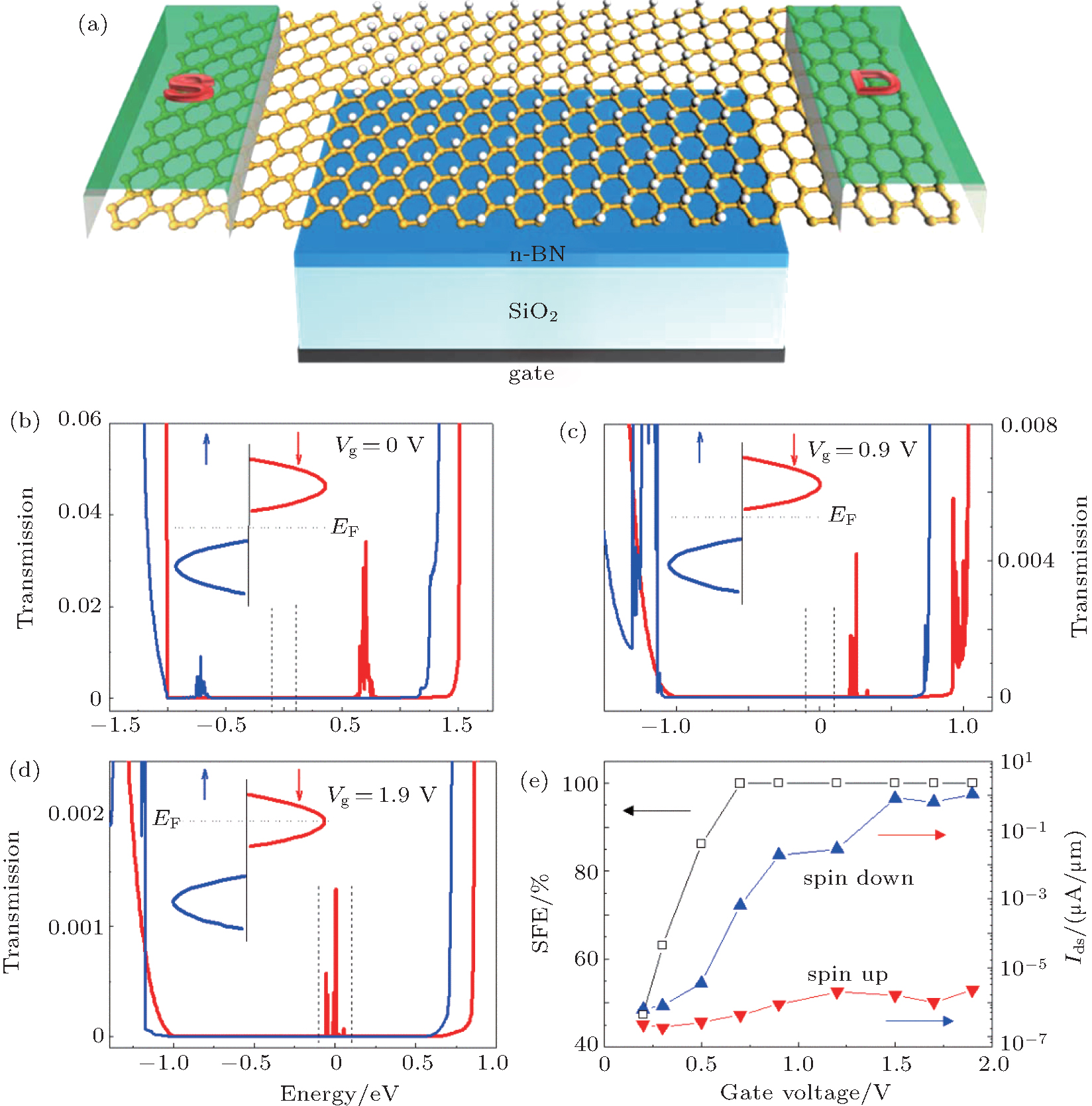 | Fig. 10. (a) Schematic diagram of two-probe model of H@silicene sheet spin-filter device with SiO2 dielectric and h-BN buffer layer. (b)– (d) The spin-polarized transmission spectra with Vg = 0, 0.9, and 1.9 V, respectively. The bias voltage is fixed at Vbias = 0.2 V. Red (blue) line stands for the spin down (up). The vertical dashed lines denote the bias voltage window. Insets are the schematic plot of the Fermi level shift with the gate voltage. (e) Spin-filter efficiency and spin-resolved current as a function of the gate voltage. Reproduced with permission from Ref. [37]. Copyright 2013 Elsevier B.V. |
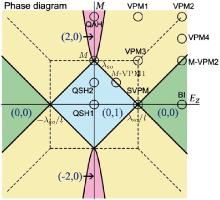
The low-energy structure of silicene is described by Dirac electrons with relatively larger spin– orbit interaction. The phase diagram of silicene as a function of electric field and exchange field has been investigated by Ezawa.[38] A QAH insulator, valley-polarized metal (VPM), QSH insulator, and band insulator (BI) all appear. They are characterized by the Chern number and spin-Chern number and/or by the edge modes of a nanoribbon. In this work, the silicene system is described by the four-band second-nearest-neighbor tight binding model:[38]

where 


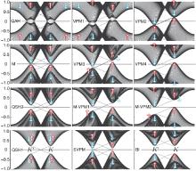
The phase diagram in the Ez– M plane is provided in Fig. 11. The topological quantum numbers are Chern number C and spin Chern number Cs. When Ez = 0 and M = 0, considering only the SOC effect, silicene is a QSH insulator ((C, Cs) = (0, 1)) with a small SOC gap of 1.55 meV, [28] much higher than that of graphene with an order of 10− 3 meV, [29] as shown in Fig. 12 (QSH1) qualitatively. Therefore, it is possible to observe the QSH state for silicene at experimentally accessible temperatures. Along the Ez axis in the phase diagram, a topological phase transition occurs, from topological insulator to trivial insulator.[39– 41] As shown in the last row of Fig. 12, the spin degrees of freedom in the band structure are degenerate in QSH1, as a consequence of both time reversal symmetry and inversion symmetry (IS). By applying a perpendicular electric field Ez, a spin splitting caused by IS-breaking is obtained.[39] At the K point, the energy gap decreases linearly as Ez increases until a critical field

is reached, where λ R1 (Ez) = α Ez with α = 10− 3 Å . Note that (α /l)2 = 10− 4 is negligible, Ec ≈ ± λ SO/l = 17 meV/Å and λ R1 is on the order of only 10 μ eV at this critical electric field. With E approaching the critical field Ec, the gap shrinks to zero, forming a Dirac-like cone near each valley (spin VPM, i.e. SVPM). In sharp contrast to the Dirac cones in graphene, where each cone is spin-degenerate, here the spin is fully polarized along the z direction at each valley. The spin-polarization profile around the K′ point is opposite to that of the K point, as required by time reversal symmetry. Therefore, in the critical phase (SVPM), the physics of the system is dominated by two nearly fully spin-polarized (with opposite polarizations) Dirac-like cones at the K and K′ points. For Ez > Ec, the energy gap reopens at each valley and drives the QSH phase into the topologically trivial band insulating phase with (C, Cs) = (0, 0).
Along the M axis, due to Ez = 0, the first Rashba interaction vanishes. The band profiles are depicted in the first column of Fig. 12. As M increases, due to the breaking of time reversal symmetry, the spin splitting occurs. The spin-up bands are lifted up while the spin-down bands are pushed down. When 
When MEz ≠ 0, in the regions where the effects of λ R1 and λ R2 are negligible, the energy spectrum is derived as

The effect of Ez is to change the mass of the Dirac electron. When increasing Ez from Ez = 0 with M fixed, the mass decreases (increases) for the Dirac cone characterized by η sz = + 1 (η sz = − 1) until Ez = λ SO/l, but the behavior becomes opposite after Ez = λ SO/l. As a result, the tip of each Dirac cone is pushed either downward or upward as indicated in Fig. 12. Consequently the valley symmetry is broken. Conducting VPM phase occupies a primary part of the phase diagram, where electrons are removed from K valley to K′ valley when Ez > 0 and M > 0. As a result, Ef is below the top of the valence band of the K valley but above the bottom of the conduction band of the K′ valley, although a band gap is opened at both the valleys. Marginal VPM (M-VPM) states appear on the phase boundaries, where the bottom of the conduction band of the K′ valley and the top of the valence band of the K valley both touch the Fermi level.
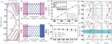
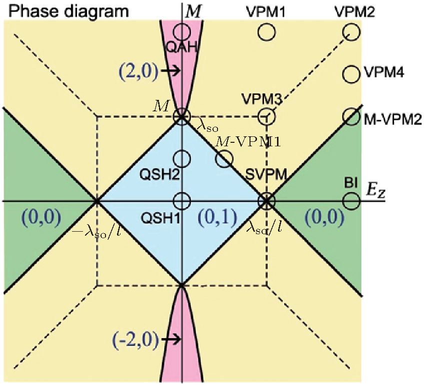 | Fig. 11. Phase diagram in the Ez– M plane. Heavy lines represent phase boundaries where the system becomes metallic. Chern and spin-Chern numbers (C, Cs) are well defined and given in insulator phases. Dotted lines represent the points where the band gap closes within the VPM phase. A circle shows a point where the energy spectrum is calculated and is shown in Fig. 12. Reproduced with permission from Ref. [38]. Copyright 2012 American Physical Society. |
Strong magnetic moments can be induced by doping 3d transition metals. Silicene decorated with certain 3d transition metals (such as vanadium) has been demonstrated to sustain a stable QAHE, using both an analytical model and first principles theory.[42] Electrically tunable topological states can also be realized in silicene doped with certain other transition metals. Silicene decorated with chemical functional groups (X– Si, X = – H, − F, − Cl, − Br, and − I) are also investigated.[43] They are trivial band insulators with larger band gaps. By applying biaxial tensile strain, X– Si can be transformed into QSH state. These findings are highly desirable for future nanoelectronic and spintronic applications.
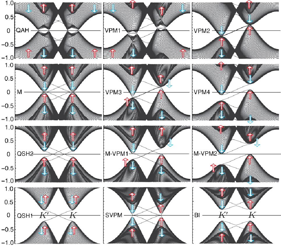 | Fig. 12. The band structure of a silicene nanoribbon at points marked in the phase diagram (Fig. 11). The vertical axis is the energy in units of t, and the horizontal axis is the momentum. We can clearly see the Dirac cones representing the energy spectrum of the bulk. Lines connecting the two Dirac cones are edge modes. The spin sz is practically a good quantum number, which we have assigned to the Dirac cones. Reproduced with permission from Ref. [38]. Copyright 2012 American Physical Society. |
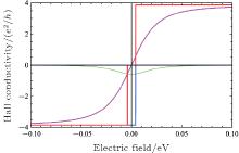
In addition to the quantum states described above, broken inversion symmetry induced by Ez could induce the quantum valley Hall (QVH) effect in silicene, in which Dirac fermions in different valleys flow to the opposite transverse edges with quantized conductivity when an in-plane electric field is applied. When Ef lies in the gap, the spin and valley Hall conductivities are obtained as[41]
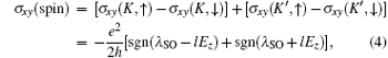
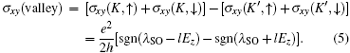
When | Ez| < | Ec| = λ SO/l, then σ xy (spin) = − e2/h and σ xy (valley) = 0, which corresponds to the QSH state, as shown and discussed in Figs. 11 and 12. When | Ez| > | Ec| = λ SO/l, then σ xy (spin) = 0 and σ xy (valley) = e2/h, which corresponds to a QVH insulating state. As shown in Fig. 13, when Ef is in the band gap, the QSH (blue) and QVH (red) conductivities undergo sharp transitions as the electric field changes. When Ef is in the conduction or valence band, this topological transition is also possible to observe, as shown in Fig. 13 (green and magenta). As the SOC in silicene is strong, the Hall plateau is not affected at finite low temperature.
 | Fig. 13. Quantum spin and valley Hall conductivities as functions of the perpendicular electric field for a fixed value of the SOI (3.9 meV). Blue and green: quantum spin Hall conductivities for the Fermi level in the band gap and the conduction band, respectively. Red and magenta: valley Hall conductivities for the Fermi level in the band gap and the conduction band, respectively. Reproduced with permission from Ref. [41]. Copyright 2013 AIP Publishing LLC. |
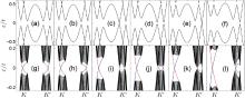
 | Fig. 14. Evolution of band structures of bulk [(a)– (f)] and zigzag-terminated [(g)– (l)] silicene as a function of extrinsic Rashba SOCλ R1 at fixed intrinsic Rashba SOC λ R2 and exchange field M. (a) λ R1 = 0. Bulk energy gaps open around the K and K′ Dirac points. The size of the bulk gap near valley K is exactly the same as that near valley K′ . (b)– (f) λ R1/t = 0.01, 0.031, 0.045, 0.067, 0.09, respectively. With increasing λ R1, the bulk gap around valley K gradually increases, while the bulk gap near valley K′ closes twice [see panels (c) and (e)] and reopens twice [see panels (d) and (f)]. (g)– (l) The valley-associated gapless edge modes at valleyK are unchanged, but those at valley K′ change; i.e., there are two or one pair of edge modes after the bulk gap reopens. Colors are used to label the edge modes localized at opposite boundaries. Other parameters in Eq. (2) are set to be  |
A new quantum state of matter — the valley-polarized QAH state is also predicted in silicene by Yao et al.[44] When the time-reversal symmetry is broken from the exchange field, the competition between intrinsic and extrinsic Rashba SOCs results in a new topological phase. When the extrinsic Rashba SOC gradually increases from λ R1/t = 0.01 to λ R1/t = 0.09, as shown in Fig. 14, the bulk band gap at valley K′ closes and reopens twice. Through analyzing the resulting Berry curvatures of the occupied valence bands, the nonzero Chern number (C = − 1) directly indicates a QAH phase, as shown in Fig. 14(d). Surprisingly, the two valleys contribute to different Chern numbers, i.e., CK = 1 but CK′ = − 2. This imbalance signals a QVH phase with valley-Chern number Cv = 3, which means the proposed state is a valley-polarized QAH state. As shown in Fig. 15, three edge states are localized at each boundary. For the upper (lower) boundary, two edge states associated with valley K′ propagate from right (left) to left (right) while one associated with valley K counterpropagates from left (right) to right (left), leading to a valley-polarized edge current.
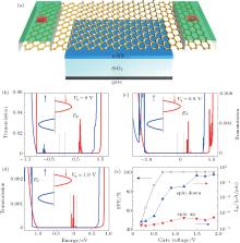
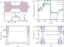
A spin-filter can also be designed based on a quantum point contact (QPC) in a silicene sheet characterized by a short and narrow constriction as shown in Fig. 16(a).[39] To make the valley degrees of freedom well separated, the zigzag edges are adopted for the whole geometry along the direction of current flow. The two opposite wide regions are in the SVPM phase with Ef > 0 to model metallic source and drain (Fig. 16(c)) and the gated constriction is in the M-VPM phase with a fixed Ez > Ec and an applied Zeeman field M = lEz − λ SO (Fig. 16(d)). An electrostatic potential barrier U(xi) is added along the current flow direction, as shown in Fig. 16(a); it is non-vanishing only in the constriction region. The resulting spin polarization as a function of the effective chemical potential, μ 0 = Ef − U0, is shown in Fig. 16(b). Through quantum transport calculations based on the iterative Green’ s function method, the QPC produces an almost fully spin-polarized current. The spin-polarization direction can be easily reversed by locally changing the potential barrier via gating control in the constriction. Such a high-efficiency, field-tunable spin-filter based on silicene takes advantage of charge carriers in the bulk system, the small Rashba SOC, and controllable spin-splitting due to IS breaking, and it is robust against weak disorder (compared with λ SO + M) and edge imperfections.
 | Fig. 15. Valley-associated edge modes for the valley-polarized QAHE. Colors are used to label the edge modes localized at opposite boundaries. Reproduced with permission from Ref. [44]. Copyright 2014 American Physical Society. |
 | Fig. 16. Tunable high-efficiency spin-filter. (a) Geometry of the spin-filter and the profile of the potential barrier U(xi). The two colors of atoms on the lattice emphasize the buckled structure. (b) Spin-polarization of the filter as a function of μ 0 in the constriction. The blue (green) line corresponds to the case of applying a potential barrier with a rectangular (smooth) shape. Panels (c) and (d) are typical dispersion relations for the wide and the constriction regions, respectively. Reproduced with permission from Ref. [39]. Copyright 2013 Macmillan Publishers Limited. |
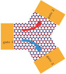
A Y-shaped spin/valley separator based on silicene, shown in Fig. 17, is proposed to separate the two spin/valley polarizations from the incoming lead 1, with one flowing to lead 2 and the other flowing to lead 3. An out-of-plane electric field, Ez > Ec, is first applied in the central silicene sheet to create a nonvanishing Berry curvature, and chemical potential μ is tuned into the conduction bands. Then by setting potentials, for example, V1 > V2 = V3, at the terminals of silicene, charge carriers acquire an anomalous velocity proportional to the Berry curvature in the transverse direction, similar to that reported by Xiao et al. in graphene.[45] By using linear response theory with negligible λ R1 and λ R2, the spin and valley Hall conductivities for Ef in the conduction band are obtained:
Thus valley and hence spin polarization imbalance at output terminals V2 and V3 are obtained (with opposite polarization between them). Therefore silicene provides an ideal platform for efficiently manipulating spin/valley degrees of freedom.
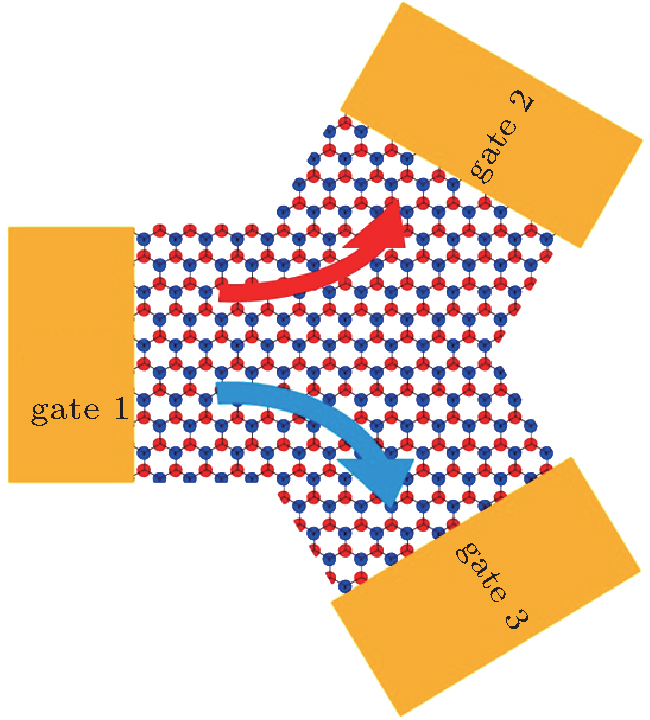 | Fig. 17. Y-shaped silicene spin-separator. Schematic of a Y-shaped separator of silicene with three local gates (leads). The current separates into gate 2 and gate 3, respectively, carrying opposite spin/valley degrees of freedom. Reproduced with permission from Ref. [39]. Copyright 2013 Macmillan Publishers Limited. |
Tremendous progress has been made in studying silicene spintronics over the past several years. Zigzag silicene nanoribbons become half-metals under the influence of a transverse electric field or in response to asymmetric edge modifications, and spin-filters and spin FETs based on them can be designed to achieve high performance. Giant magnetoresistance is obtained in zigzag silicene nanoribbons either by utilizing the switching between different magnetic states or the symmetry-dependent transport property. Half-metallicity can also be achieved in semihydrogenated silicene by applying an out of plane gate voltage. The spin-filters designed by utilizing half-metallicity in semihydrogenated silicene and by utilizing the peculiar topological quantum states in pristine silicene are predicted to be able to deliver nearly 100% spin-polarized current. By adjusting an electric field and/or an exchange field, the quantum spin Hall effect, quantum anomalous Hall effect, valley-polarized quantum anomalous Hall effect, or quantum valley Hall effect are predicted to be realizable in pristine silicene. However, so far, no experimental observations have been reported despite all these fascinating theoretical predictions. Because extreme surface sensitivity greatly limits both the isolation and device fabrication possibilities of silicene, experimental research on silicene, whether fundamental or device-oriented, has been extremely difficult. Despite these difficulties, very recently, a silicene FET operating at room temperature was reported to have been fabricated via a growth-transfer-fabrication process.[23] This experimental breakthrough is expected to strongly stimulate researchers in the field to continue looking for methods to solve the known problems and making further improvements. We believe that silicene spintronics will be made a reality one day, as more mature experimental techniques are developed.
| 1 |
|
| 2 |
|
| 3 |
|
| 4 |
|
| 5 |
|
| 6 |
|
| 7 |
|
| 8 |
|
| 9 |
|
| 10 |
|
| 11 |
|
| 12 |
|
| 13 |
|
| 14 |
|
| 15 |
|
| 16 |
|
| 17 |
|
| 18 |
|
| 19 |
|
| 20 |
|
| 21 |
|
| 22 |
|
| 23 |
|
| 24 |
|
| 25 |
|
| 26 |
|
| 27 |
|
| 28 |
|
| 29 |
|
| 30 |
|
| 31 |
|
| 32 |
|
| 33 |
|
| 34 |
|
| 35 |
|
| 36 |
|
| 37 |
|
| 38 |
|
| 39 |
|
| 40 |
|
| 41 |
|
| 42 |
|
| 43 |
|
| 44 |
|
| 45 |
|