


Chemical modification of silicene
[Wang Ronga) , Xu Ming-Shengb) , Pi Xiao-Dong†c)  ]
]
]
|
|


†Corresponding author. E-mail: xdpi@zju.edu.cn
*Project supported by the National Basic Program of China (Grant No. 2013CB632101), the National Natural Science Foundation of China (Grant Nos. 61222404 and 61474097), and the Fundamental Research Funds for the Central Universities of China (Grant No. 2014XZZX003-09).
Silicene is a two-dimensional (2D) material, which is composed of a single layer of silicon atoms with sp2–sp3 mixed hybridization. The sp2–sp3 mixed hybridization renders silicene excellent reactive ability, facilitating the chemical modification of silicene. It has been demonstrated that chemical modification effectively enables the tuning of the properties of silicene. We now review all kinds of chemical modification methods for silicene, including hydrogenation, halogenation, organic surface modification, oxidation, doping and formation of 2D hybrids. The effects of these chemical modification methods on the geometrical, electronic, optical, and magnetic properties of silicene are discussed. The potential applications of chemically modified silicene in a variety of fields such as electronics, optoelectronics, and magnetoelectronics are introduced. We finally envision future work on the chemical modification of silicene for further advancing the development of silicene.
The rapid development of graphene has been arousing great interest in producing all kinds of two-dimensional (2D) layered materials. Silicene, the 2D honeycomb allotrope of silicon, has recently attracted intensive attention due to its unique properties.[1, 2] Charge carriers in silicene behave like massless Dirac fermions, whose velocity near the Fermi level is estimated to be on the order of 106 m/s. This so-called Fermi velocity is comparable to that of graphene.[3, 4] The sp2– sp3 hybridization of Si atoms in silicene leads to a buckled structure of silicene, distinguishing silicene from the planar graphene. Such a distinct structure of silicene makes its properties different from those of graphene, creating new possibilities for manipulating the dispersion of electrons and enabling the tuning of the electronic and magnetic properties of silicene by external fields.[5– 7] Silicene is predicted to possess strong spin– orbit coupling, which should result in detectable quantum spin Hall effect.[8] Moreover, silicene is essentially compatible with current Si-based technologies, [9] giving rise to great promise in the electronic application of silicene.[10– 12] Silicene field-effect transistors (FETs) exhibiting an ambipolar behavior with carrier mobilities around 100 cm2/V· s at room temperature have already been demonstrated.[11]
For the practical applications of silicene, the opening and controlling of the bandgap of silicene are critical.[12] The reactive surface of silicene enables chemical modification to tune the band structure of silicene[13] by means of inorganic surface modification, [14– 38] organic surface modification, [39– 45] oxidation, [46– 53] doping, [54– 60] and formation of 2D hybrids.[61– 68] Experimental investigation on the chemical modification of silicene is still at the preliminary stage, [31, 40– 47] while a number of theoretical investigations have been carried out to understand the chemical modification of silicene. The present review deals with the progress in the research on the chemical modification of silicene. Theoretical studies on the effects of hydrogenation, halogenation, organic surface modification, oxidation, doping and formation of 2D hybrids on the electronic, optical and magnetic properties of silicene will be introduced in detail. Experimental researches that are mainly concerned with the hydrogenation, oxidation, and organic surface modification of silicene will be discussed. In the end, remarks and outlook are provided for the study of the chemical modification of silicene.
Hydrogenation is the process that hydrogen (H) atoms passivate silicene via the unpaired electrons of Si atoms.[16] Hydrogenation has been proved to be an effective chemical modification method to gain interesting properties for silicene. Owing to the fine reversibility and excellent controllability of hydrogenation, a number of efforts have recently been devoted to tailoring the properties of silicene by hydrogenation.[61– 63] In this section, we will deal with the formation, structures, electronic properties, optical properties, and magnetic properties of hydrogenated silicene with full and half hydrogen passivation.
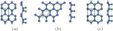
Figure 1 shows that there are five possible atomic configurations (top-like, chair-like, boat-like, Z-line, and A-line) for fully hydrogenated silicene.[15, 17, 18] Theoretical researchers have investigated the formations and stabilities of fully hydrogenated silicene with different configurations by comparing their formation and binding energies. The formation energy (Ef) and binding energy (Eb) of fully hydrogenated silicene were calculated by using Ef = Et− Es− nHEH2/2 and Eb = Et− nSi− nHEH, respectively. Et, Es, EH2, EH, and ESi were the total energies of fully hydrogenated silicene, silicene, hydrogen gas, a hydrogen atom, and a silicon atom, respectively. nH and nSi were the numbers of H atoms and Si atoms, respectively.[15, 17, 18] It was found that the values of Ef and Eb were negative for all the structures of fully hydrogenated silicene, indicating the hydrogenation process was exothermic and the structures of fully hydrogenated silicene were stable.[15, 17, 18] The values of Ef and Eb for fully hydrogenated silicene with the chair-like configuration were the lowest. Therefore, it was concluded that the chair-like configuration was the most possible configuration for fully hydrogenated silicene in terms of formation and stability.[15, 17]
 | Fig. 1. Optimized structures of fully hydrogenated silicene with (a) top-like, (b) chair-like, (c) boat-like, (d) Z-line, and (e) A-line configurations. Silicon and hydrogen atoms are denoted by blue and pink balls, respectively.[15, 17, 18] |
Figure 2 shows that half-hydrogenated silicene can be generated by the hydrogenation only at one side of silicene. Like what happens to the full hydrogenation of silicene, the zigzag, chair-like, and boat-like configurations may form during the half hydrogenation of silicene (Fig. 2).[18] Calculations on the Ef and Eb confirmed that the structures of half-hydrogenated silicene can all be formed and stable, as evidenced by the negative values of Ef and Eb. The chair-like configuration is the most likely to form because of the lowest value of Ef for half-hydrogenated silicene.[18]
 | Fig. 2. Optimized structures of half-hydrogenated silicene with (a) zigzag, (b) chair-like, and (c) boat-like configurations. Silicon and hydrogen atoms are denoted by blue and green balls, respectivelly.[18] |
Although hydrogenated silicene with the chair-like configuration is the most likely to form, the reaction energy barrier for the hydrogenation of silicene is quite high (∼ 1.8 eV).[19, 20] It has been theoretically demonstrated that the energy barrier can be reduced by applying external tensile strain or electric field.[19, 20] Wu et al. have demonstrated that the energy barrier for the hydrogenation of silicene could be reduced by exerting biaxial strain or uniaxial tensile strain along the armchair direction of silicene.[19] Wu et al.’ s results demonstrated that applying a perpendicular electric field could also facilitate the hydrogenation of silicene.[20] However, the external tensile strain or electric field changes the electronic structure of hydrogenated silicene because of the redistribution of atomic charges.[19, 20] It should be pointed out that tensile strain may also affect the electronic structure of silicene by changing the electron– phonon coupling.[21, 22]
Since hydrogenated silicene is the most likely in the chair-like configuration, people usually focus on the properties of the chair-like hydrogenated silicene. The geometrical properties of fully hydrogenated silicene obtained with density functional theory (DFT) calculations are tabulated in Table 1. The values of buckling distance (Δ ), Si– Si bond length (〈 Si– Si〉 ), Si– Si– Si bond angle (∠ (Si– Si– Si)), and Si– H bond length (〈 Si– H〉 ) of fully hydrogenated silicene are 0.72 Å – 0.74 Å , 2.31 Å – 2.36 Å , 110° , and 1.50 Å – 1.52 Å , respectively.[15– 18, 23, 24] The buckling distance and Si– Si bond length of fully hydrogenated silicene are larger than those of silicene, while the Si– Si– Si bond angle is smaller than that of silicene. These structural changes indicate the hydrogenation-induced transition from mixed sp2– sp3 hybridization toward sp3 hybridization in fully hydrogenated silicene for Si atoms.
| Table 1. Structural properties such as the buckling distance (Δ ) of Si, the bond length of Si– Si, the bond length of Si– H, the bond angle of Si– Si– Si, and bandgaps for the structures of silicene, fully hydrogenated silicene (FH-silicene) and half-hydrogenated silicene (HH-silicene). |
Figure 3 shows that fully hydrogenated silicene is an indirect-bandgap semiconductor with the valence-band maximum (VBM) and the conduction band minimum (CBM) appearing at the Γ and M points, respectively. The bandgap (Eg) obtained by DFT calculations with generalized gradient approximation (GGA) is 2.0 eV– 2.4 eV (Table 1).[15– 18, 23, 24] DFT calculations usually underestimate the bandgaps of semiconductors because of the neglect of quasiparticle and excitonic effects.[70] Researchers have also performed hybrid Heyd– Scuseria– Ernzerhof (HSE) calculations as well as G0W0 (GW) many-body perturbation method for fully hydrogenated silicene. They showed that the accurate bandgaps of fully hydrogenated silicene were in a range of 3.5 eV– 4.0 eV (Table 1).[17, 18, 25]
 | Fig. 3. Band structure of fully hydrogenated silicene. Quasiparticle corrections (GW approximation) to the DFT energies are indicated as red dots. The Fermi level is at the energy of zero.[25] |
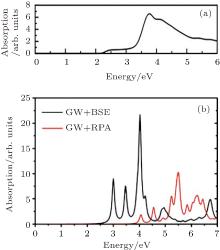
The optical absorption spectra of fully hydrogenated silicene, calculated by DFT and GW approximation are shown in Figs. 4(a) and 4(b). The absorption spectrum of fully hydrogenated silicene, obtained with the DFT calculation shows an absorption onset at 2.2 eV, which is consistent with the bandgap of fully hydrogenated silicene calculated by using DFT. The absorption peak is located at 3.7 eV.[26] Wei and Jacob calculated the optical absorption spectra of fully hydrogenated silicene by using GW approximation with random phase approximation (GW, + , RPA) and Green’ s function perturbation theory (GW, + , BSE).[27] The shape of the absorption spectrum obtained with GW, + , RPA was different from that obtained with DFT calculations because of the large self-energy correlations of electrons. The absorption onset obtained with GW, + , RPA located at ∼ 4 eV was consistent with the bandgap. Since silicene is a 2D material, the excitonic effect may introduce remarkable change in the optical properties of fully hydrogenated silicene. Therefore, Wei and Jacob calculated the optical absorption spectrum of fully hydrogenated silicene by using GW, + , BSE, which included the excitonic correlations of electrons and holes. Their results demonstrated that the excitonic effect significantly blueshifted the onset of the absorption spectrum of fully hydrogenated silicene. Strongly bound excitons below the onset of single-particle transition continuum appeared (Fig. 4(b)). The inclusion of
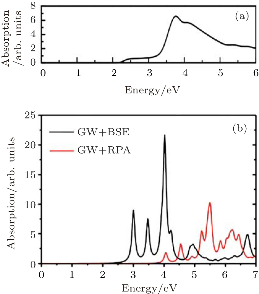 | Fig. 4. Optical absorption spectra of fully hydrogenated silicene calculated with (a) DFT calculations and (b) GW approximations with (GW + BSE) and without (GW + RPA) considering the excitonic effect.[26, 27] |
excitonic correlations between electrons and holes significantly redistributes the oscillator strength by introducing excitonic resonances. Since the excitonic effect significantly affects the optical properties of fully hydrogenated silicene, interactions of electrons and holes should be considered during the calculation of the optical absorption spectrum of fully hydrogenated silicene.[27]
Based on its electronic and optical properties, fully hydrogenated silicene holds potential in optoelectronic applications in the ultraviolet (UV) region.[27– 29] Although fully hydrogenated silicene is an indirect-bandgap semiconductor without linear band dispersion, a heterobilayer based on silicene and fully hydrogenated silicene exhibits linear band dispersion character with a sizable band gap opening (44 meV– 61 meV) and high carrier mobility (105 cm2· V− 1· s− 1).[30] Therefore, fully hydrogenated silicene may be used as an inert substrate for silicene to make silicene transistors.
Qiu et al. investigated the hydrogenation of silicene by using scanning tunneling microscopy (STM).[31] They synthesized silicene by evaporating silicon to a single-crystal Ag (111) substrate. They then exposed silicene to a high-purity H2 gas at room temperature to generate hydrogenated silicene. It was found that the superstructure of silicene was 3× 3 with the hexagonal arrangement of triangular structures around dark centers as shown in Fig. 5(a).[31] The structural model of the 3× 3 silicene indicated that each 3× 3 unit cell was composed of two triangular half unit cells (Fig. 5(b)). In each 3× 3 unit cell there were 6 upper-buckled Si atoms indicated by red balls and 12 lower-buckled Si atoms indicated by yellow balls. The exposure of silicene to 900-L H2 gas at room temperature resulted in hydrogenated silicene with invariable superstructure and rearranged buckling configuration. As shown in Fig. 5(c),
 | Fig. 5. (a) The STM image and (b) the structural model of the clean silicene (c) The STM image and (d) the structural model of the hydrogenated silicene.[31] |
there were two different triangular half unit cells in each 3× 3 unit cell of the hydrogenated silicene. As shown in the structural model of the hydrogenated silicene, one of the half unit cells had 6 bright spots while the other had only 1 bright spot in the middle (Fig. 5(d)).[31] The structure of hydrogenated silicene did not change when the H2 dosage increased. This indicated that fully hydrogenated silicene was formed. Moreover, the dehydrogenation of fully hydrogenated silicene could occur by annealing at ∼ 450 K. The superstructure and the buckling configuration of dehydrogenated silicene were the same as those of pristine silicene.
Half-hydrogenated silicene has the advantages of bandgap opening and novel magnetoelectric properties. Researchers usually focus on the properties of the chair-like half-hydrogenated silicene, because half-hydrogenated silicene is the most likely in the chair-like configuration. We now introduce the geometrical, electronic, and magnetic properties of half-hydrogenated silicene. Table 1 shows that the values of buckling distance (Δ ), Si– Si bond length (〈 Si– Si〉 ), and Si– H bond length (〈 Si– H〉 ) of half-hydrogenated silicene with the chair-like configuration are 0.61 Å – 0.69 Å , 2.34 Å – 2.35 Å , and 1.51 Å – 1.52 Å , respectively.[18, 32, 33] The buckling distance and Si– Si bond length of half-hydrogenated silicene are smaller than those of fully hydrogenated silicene, indicating that half-hydrogenated silicene is composed of mixed sp2– sp3 bonded Si atoms. After half hydrogenation, half Si atoms in silicene are passivated by H atoms via σ bonds, leaving electrons in unsaturated Si atoms localized and unpaired.
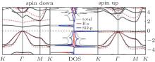
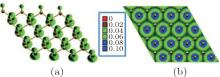
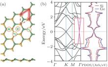
The band structure of half-hydrogenated silicene obtained with GGA calculations shows an indirect bandgap of 0.84 eV– 0.95 eV (Table 1).[18, 32, 33] However, the hybrid functional (HSE06) calculations indicate that half-hydrogenated silicene is a direct bandgap semiconductor with a bandgap of 1.79 eV, [18] which is indicated in Fig. 6. As shown in the partial density of states (PDOS) and spatial spin-density distribution, states near the Fermi energy level are mainly derived from the p orbital of unsaturated Si atoms for half-hydrogenated silicene (Figs. 6 and 7).[18, 32]
The spin-polarized DOS for the spin-up channel is significantly different from that for the spin-down channel (Fig. 6), indicating distinct magnetism in half-hydrogenated silicene. This is because the pz electrons of unsaturated Si atoms are unpaired and localized, leading to a strong tendency to magnetize the half-hydrogenated silicene. However, the pz electrons of H-passivated Si atoms have no contribution to the magnetism (Fig. 7).[18, 32] Pan et al. theoretically investigated the transport properties of an FET, in which half-hydrogenated silicene was used as the channel material (Fig. 8(a)). The study showed that the on/off current ratio of the FET was as high as 106, which is qualified for high-speed complementary MOS-like logic
 | Fig. 6. The band structure of half-hydrogenated silicene. The black solid and red dashed lines represent GGA and hybrid HSE06 results, respectively. The Fermi levels are shown by black dashed lines. The total and partial DOS of Si are given.[18] |
 | Fig. 7. Spatial spin-density distribution of half-hydrogenated silicene. Side view and top view are presented in panels (a) and (b), respectively.[32] |
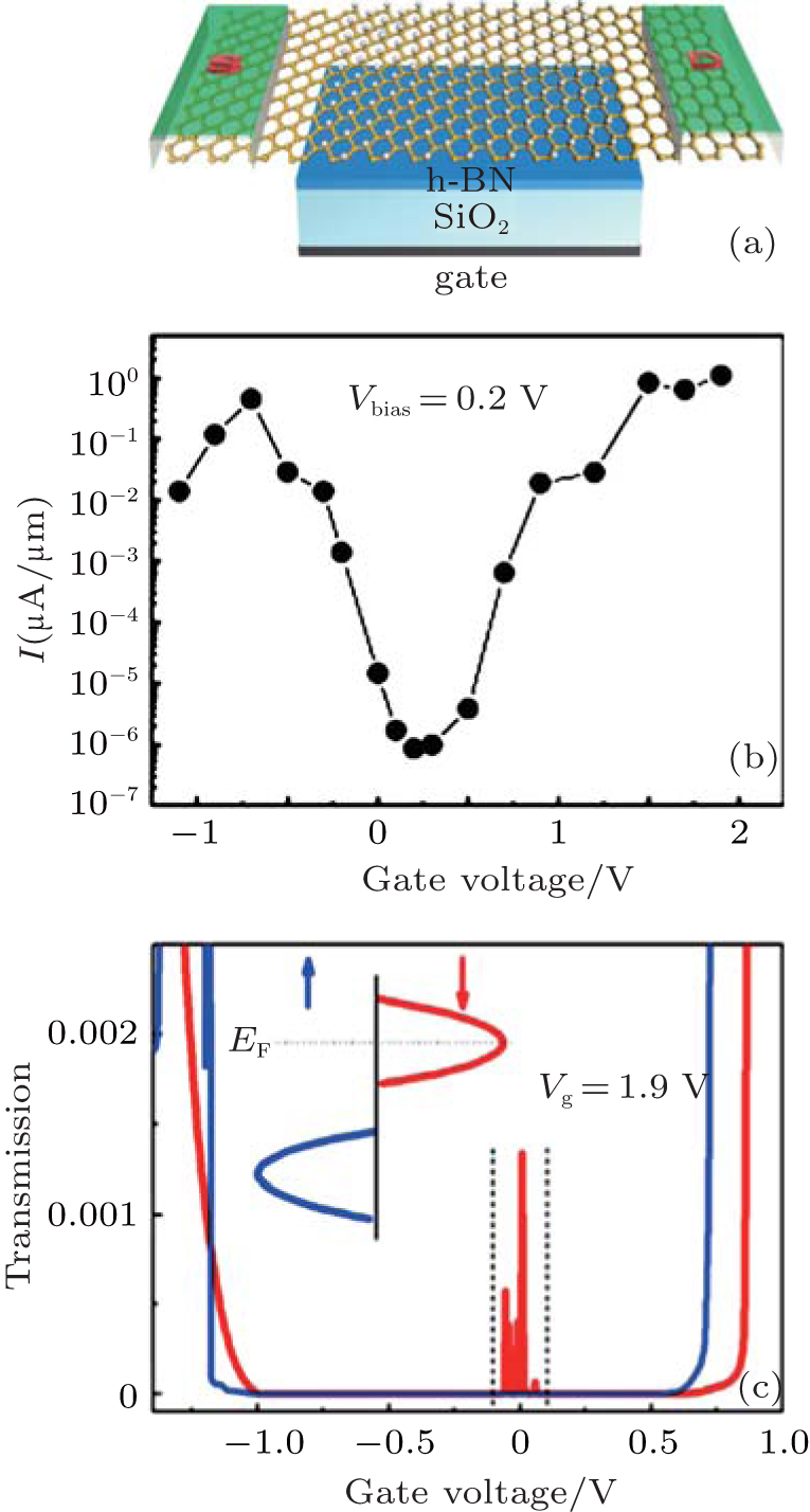 | Fig. 8. (a) Schematic diagram of an FET based on half-hydrogenated silicene. The gate dielectric material is SiO2, and h-BN is the buffer layer. The electrodes are made of semi-infinite silicene. The channel of half-hydrogenated silicene is 31.52-Å long. (b) Calculated transfer characteristic at a bias voltage of 0.2 V for the FET. (c) Spin-polarized transmission spectra with a gate voltage of 1.9 V. The bias voltage is fixed at 0.2 V. Red (blue) line represents the spin down (up). The inset shows the schematic plot of the Fermi energy level shift with the gate voltage.[33] |
applications[33, 71] (Fig. 8(b)). In addition, they predicted a spin-polarized current in the FET based on half-hydrogenated silicene. The spin-filter efficiency increased with the increase of gate voltage and reached 100% at a gate voltage of 1.9 V (Fig. 8(c)).[33] Tao et al. have recently fabricated FETs in which silicene was used as a channel material.[11] The on/off current ratios of their transistors were < 10. They obtained the carrier mobility of ∼ 100 cm2· V− 1· s− 1. Such a breakthrough in silicene-based FETs has laid a foundation for exploring all kinds of novel FETs based on chemically modified silicene including half-hydrogenated silicene.
Halogen (F, Cl, Br, and I) atoms may passivate the surfaces of all kinds of Si materials such as bulk Si, [72, 73] Si nanowires, [74, 75] and Si quantum dots.[76, 77] As a novel Si material, silicene may be subject to halogen passivation at the surface as well. Halogenation is the process that halogen atoms passivate silicene via the unpaired electrons of Si atoms at the surface. In the following we will introduce the structural, electronic, optical, and magnetic properties of halogenated silicene with full and half passivation.
Like what happens to the fully hydrogenation of silicene, the top, chair-like, boat-like, Z-line, and A-line configurations may form during the full halogenation of silicene. The formation energies of fully halogenated silicene with these configurations are negative, indicating that they may be produced in the point of view of thermodynamics. The formation energy of fully halogenated silicene with the chair-like configuration is the lowest. Thus, it can be stated that the chair-like halogenated silicene most likely formed.[35] For fully halogenated silicene with a specific configuration, the formation energy increases in the order of F, Cl, Br, and I. This means that halogenation is less likely to occur as the atomic number of the halogen element increases.[35]
 | Fig. 9. Optimized structures of half-fluorinated silicene with (a) zigzag, (b) boat-like, and (c) chair-like configurations with both top and side views. Silicon and fluorine atoms are denoted by yellow and blue balls, respectively.[36] |
As to the half halogenation of silicene, Wang et al. investigated the half-fluorination of silicene with zigzag, boat-like, and chair-like configurations.[36] The optimized structures of half-fluorinated silicene with these configurations are shown in Fig. 9. They found that half-fluorinated silicene with these configurations were stable in the point of view of thermodynamics and dynamics. The Ef of half-fluorinated silicene with the zigzag configuration is the lowest, indicating the zigzag configuration is most likely to form.
We first discuss the geometrical, electronic, and optical properties of fully halogenated silicene with the chair-like configuration. The geometrical properties of fully halogenated silicene are summarized in Table 2. The buckling distances of halogenated silicene are larger than that of silicene, implying that the hybridizations in halogenated silicene are closer to sp3 hybridization than that in silicene.[15, 27, 34– 36] The lengths of Si– Si bonds in halogenated silicene are larger than those in silicene and fully hydrogenated silicene. The bond length of Si– X (X = F, Cl, Br, and I) increases with the increase of the atomic number of the halogen element, which is consistent with the change in the halogen-atom size.[34, 35]
All the fully halogenated silicene has a direct bandgap with both the VBM and CBM at the Γ point. The bandgap of fully halogenated silicene ranges from 0.54 eV to 2.76 eV, depending on halogen elements and calculation methods.[15, 28, 34, 35, 37] As the passivating element changes from F to I, the bandgap of halogenated silicene first increases and then decreases. The bandgap of chlorinated silicene is largest.[34, 35] Zhang et al. calculated the element-projected band structures of halogenated silicene.[35] Their results indicated that the CBM was insensitive to the halogen element, while the effect of the halogen element was appreciable for the VBM. Figure 10 shows that the orbital contributions of the halogen element to the CBM are less than 20%. However, the orbital contributions of the halogen element to the VBM are < 20%, 20%, 40%, and 80% for fluorination, chlorination, bromination, and iodination, respectively.[35] Gao et al. have explained the orbital contributions by calculating the charge density distributions of the CBM and VBM states at the Γ point.[34] The CBM mainly originates from the antibonding state of the p orbitals of Si atoms, while the VBM originates from the p orbitals of Si atoms and halogen atoms. As the atomic number of the halogen element increases, the VBM is more significantly derived from the p orbitals of halogen atoms, indicating the formation of surface states upon halogenation. The interaction among the surface states is responsible for the dispersion of the CBM and VBM, and thus the opening of the bandgap.[34]
| Table 2. Structural properties such as the buckling distance (Δ ) of Si, the bond length of Si– Si, the bond length of Si– X (X = F, Cl, Br, and I), and bandgaps of fully halogenated silicene. The methods used to calculate the bandgaps (GGA, M06L, VDW-DF, HSE, LDA, and GW) have been indicated. |
 | Fig. 10. Band structures and charge density distributions of the CBM (right upper) and the VBM (right lower) states at the Γ point for silicene halogenated with (a) F, (b) Cl, (c) Br, and (d) I.[34, 35] |
The effective carrier masses of fully halogenated silicene in certain directions are comparable to those of silicon.[35] Taking advantage of the tunable bandgap, relatively high carrier mobility and compatibility with silicon, fully halogenated silicene holds potential for electronic and optoelectronic applications.
Wang et al. have investigated the properties of half-fluorinated of silicene with the zigzag, boat-like, and chair-like configurations.[36] They found that the electronic and magnetic properties of half-fluorinated silicene rigidly depended on the atomic configurations. Half-fluorinated silicene with zigzag and boat-like configurations are direct bandgap semiconductors with both VBM and CBM located at the Γ point. The GGA (HSE03) calculated bandgaps are 0.19 (0.41) eV and 0.40 (0.82) eV for the structures of half-fluorinated silicene with the zigzag and boat-like configurations, respectively. Wang et al. have explained why half-fluorinated silicene with zigzag or boat-like configurations was semiconducting. As shown in Fig. 11(a), the VBM of half-fluorinated silicene with the zigzag configuration results from both the σ bonding states of Si– Si bonds and the π bonding states of unsaturated Si– Si bonds, while its CBM mainly originates from the pz orbitals of unsaturated Si atoms and the anti-bonding states of Si– F bonds. For half-fluorinated silicene with the boat-like configuration, the VBM is only composed of the σ bonding states of Si– Si bonds. The CBM is composed of the pz orbitals of unsaturated Si atoms and the anti-bonding states of Si– F bonds (Fig. 11(b)). Thus, the weakening of the sp2– sp3 mixed coupling between Si atoms results in the semiconducting characteristics of half-fluorinated silicene with zigzag and boat-like configurations. The magnetic property of half-fluorinated silicene with the chair-like configuration is similar to that of half-hydrogenated silicene. The unpaired and localized pz electrons of unsaturated Si atoms result in spin
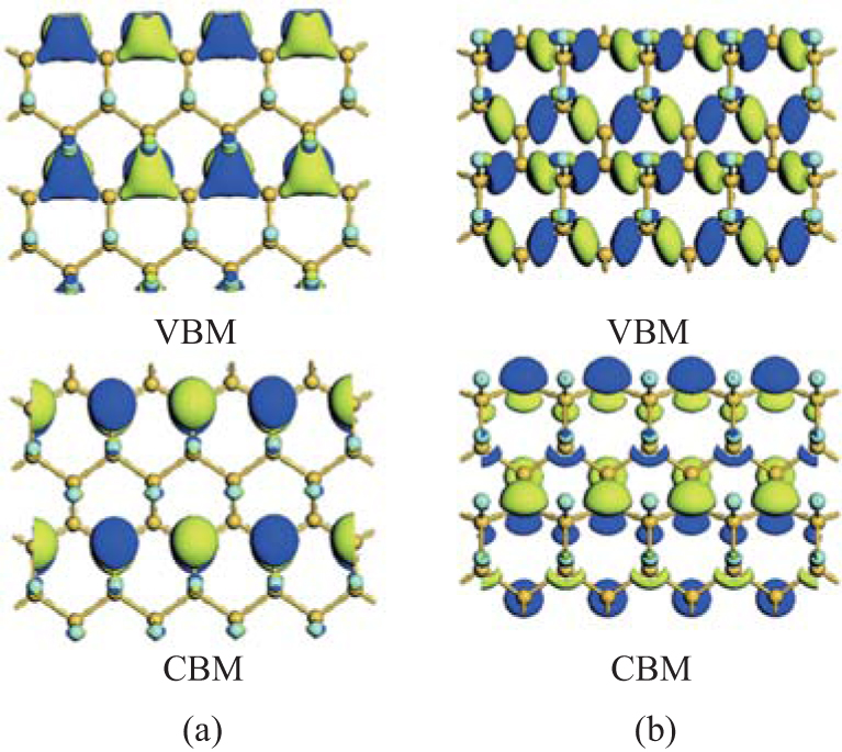 | Fig. 11. Partial charge densities of VBM and CBM for half-fluorinated silicene with (a) zigzag and (b) chair-like configurations.[36] |
polarization, which causes half-fluorinated silicene with the chair-like configuration to be antiferromagnetic.[36]
Zheng and Zhang have studied the properties of half-brominated silicene with the chair-like configuration.[38] Figure 12 shows its band structure, which indicates that it is semi-metallic. The energy bands of the spin-up channel close to the Fermi level exhibit a semiconducting behavior, while those of the spin-down channel close to the Fermi level indicate a metallic behavior (Fig. 12). Therefore, 100% spin-polarized current can be obtained in half-brominated silicene, offering a feasible method of constructing spin devices based on silicene.[38]
Nakano et al. have demonstrated the synthesis of silicene by the chemical exfoliation of calcium disilicide (CaSi2).[78] CaSi2 has a hexagonal layered structure consisting of alternating Ca layers and corrugated silicon layers. The chemical exfoliation of CaSi2 followed by HF rinsing leads to hydrogenated silicene.[40] Nakano et al. carried out hydrosilylation, aminization, and phenylation for hydrogenated silicene to prevent it from oxidizing, rendering the dispersibility of silicene in organic solvents, and tailoring the optical properties of silicene.[41– 43] Figure 13 schematically shows Nakano et al.’ s synthesis and organic surface modification of hydrogenated silicene.[40– 43, 78]
Nakano et al. found that their hydrogenated silicene was of stacked multi-layers. Hydrosilylated silicene was of single layer due to the steric hindrance of organic ligands. Moreover, hydrosilylation blueshifted the absorption onset of exfoliated silicene to 4.2 eV.[41] Aminizated silicene was found to be
 | Fig. 13. Schematic diagram of the synthesis and organic surface modification of hydrogenated silicene.[40– 43, 78] |
stacked to form multi-layers. Aminization introduced negligible effect on the absorption onset of hydrogenated silicene.[42] Phenylation separated hydrogenated silicene to be of single-layered structure.[43] However, whether the change in the absorption spectrum was really induced by the hydrosilylation-induced surface chemistry was not clear because the number of the layers of hydrogenated silicene could not be well controlled.
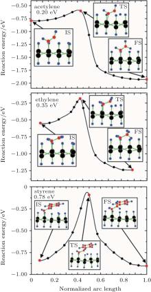
Theoretical study on the organic surface modification of silicene mainly deals with the formation and the properties of organically surface-modified silicene. Rubio-Pereda and Takeuchi have calculated the reaction energy barriers for the reactions between hydrogenated silicene and organic molecules such as acetylene, ethylene, and styrene to evaluate the possibilities of the reactions.[44] The potential energy surface along the minimum energy path (MEP) that connects the intermediate state (IS), transition state (TS), and final state (FS) in a reaction has been considered. The IS, TS, and FS correspond to the formation of an Si– C bond, H abstraction, and the formation of a new C– H bond, respectively. Figure 14 shows that during the reactions of acetylene, ethylene, and styrene with hydrogenated silicene, the IS and FS are energetically more favorable than the TS. For acetylene, ethylene, and styrene, the energy barriers of 0.20, 0.35, and 0.78 eV for H abstraction need to be circumvented to reach the FS of a reaction, respectively. The H-abstraction energy barriers are comparable to or even smaller than those for the reactions of acetylene, ethylene, and styrene with hydrogenated bulk Si (111) (0.54, 0.71, and 0.67 eV, respectively). The organic surface modification of hydrogenated bulk Si (111) has already been experimentally demonstrated. Therefore, organic surface modification is also possible for hydrogenated silicene.[44]
Wang et al. have recently investigated the geometrical structures, band structures, and optical absorption of hydrosilylated, alkoxylated, aminated, and phenylated silicenes by means of DFT calculations.[39] Propylene (CH2= CH– CH3), ethanol (CH3– CH2– OH), ethylamine (CH3– CH2– NH2), and phenylmagnesium bromide (C6H5– MgBr) were chosen for the simulations of hydrosilylation, alkoxylation, aminization, and phenylation of silicene, respectively. Silicene was in fact initially passivated by hydrogen atoms to facilitate
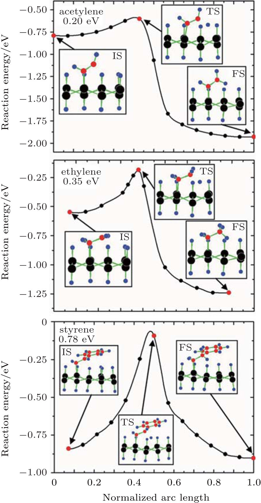 | Fig. 14. Potential energy surface along the MEP for the reactions of: (a) acetylene, (b) ethylene, and (c) styrene with the H-silicene. Silicon, carbon, and hydrogen atoms are represented by black, red, and blue balls, respectively.[44] |
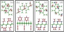
all the organic surface modifications. The surface coverage of organic ligands was consistent with the experimentally observed organic surface coverage of 33%. The optimized structures of hydrosilylated, phenylated, alkoxylated, and aminated silicene are shown in Fig. 15. It was found that organic surface modification led to the increase of the buckling distance of hydrogenated silicene, while causing the angles of bonds in the honeycomb structure of silicene to decrease. As shown in Fig. 16, hydrosilylated and phenylated silicenes were indirect bandgap semiconductors with the bandgap energies of 1.8 eV and 2.0 eV, respectively. Alkoxylated and aminated silicenes were direct-bandgap semiconductors each with a bandgap energy of ∼ 1.7 eV. The authors also calculated the optical absorption spectra of hydrogenated silicene and organically surface modified silicene. For hydrogenated silicene, the absorption onset was at ∼ 2.2 eV. The prominent absorption peak appeared at 3.7 eV. Hydrosilylation, phenylation, alkoxylation, and amination redshifted the absorption onset by 0.4, 0.2, 0.5, and 0.5 eV, respectively. However, the shift of the prominent absorption peak induced by organic surface modification was relatively small (in a range from 0.1 eV to 0.2 eV). The optical absorption demonstrated by Wang et al. qualitatively agrees with experimental results obtained by Nakano et al. The shapes of the absorption spectra for hydrosilylated and aminated silicenes were consistent with those obtained by photocurrent measurements. The experimentally obtained absorption onset of phenylated and hydrosilylated silicenes are ∼ 3 eV and ∼ 2.7 eV, respectively. The calculated absorption onset of ∼ 2 eV (1.8 eV) for phenylated (hydrosilylated) silicene was within the range underestimated by the DFT calculations. Therefore, it can be concluded that the changes in the optical properties after organical surface modification is actually caused by surface chemistry.
 | Fig. 15. Optimized structures of (a) hydrosilylated silicene, (b) phenylated silicene, (c) alkoxylated silicene, and (d) aminated silicene. Both top and side views of silicene and organically surface-modified silicene are shown. Si, H, C, O, and N atoms are denoted by green, white, red, blue, and purple balls, respectively.[39] |
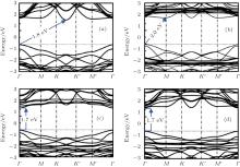
 | Fig. 16. Band structures of (a) hydrosilylated silicene, (b) phenylated silicene, (c) alkoxylated silicene, and (d) aminated silicene. Energy is shifted so that the Fermi level is at 0 eV.[39] |
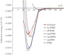
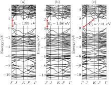
Spencer et al. calculated the interaction between phenylated silicene nanosheets and the effect of the interaction on the electronic structure of phenylated silicene.[45] Firstly, they compared the adhesion energies for phenylated silicene with different separation distances using the PBE functional, the Grimme potential, and the different DFT-vdWs (van der Waals) functionals. Figure 17 shows that there were negligible interactions between phenylated silicene nanosheets at all separation distances when the PBE functional was employed. The adhesion energy was significantly stronger as the DFT-D2 Grimme and vdW-DF2 methods were used, although the adhesion was still very weak. The optB88 gave the strongest adhesion energy at a separation distance of 10.14 Å . The authors then calculated the band structures of phenylated silicene with different separation distances using the optB88 functional. As shown in Fig. 18(a), phenylated silicene with infinite (27.64 Å ) separation distance had a direct bandgap of 1.99 eV. This result was different from Wang et al.’ s, [39] in which the separation distance of phenylated silicene nanosheets was 20 Å (which also could be regarded as infinite separation distance). Wang et al. used the PBE functional to calculate the band structure of phenylated silicene without considering van der Waals (vdWs) interactions. In contrast, vdWs interactions were concerned in Spencer et al.’ s work with the optB88 functional. Therefore, we can see that vdWs interactions introduced remarkable changes in the electronic properties of
 | Fig. 17. Calculated adhesion energy curves for phenylated silicene with different separation distances. Different functionals used in the calculations are indicated in the figure.[45] |
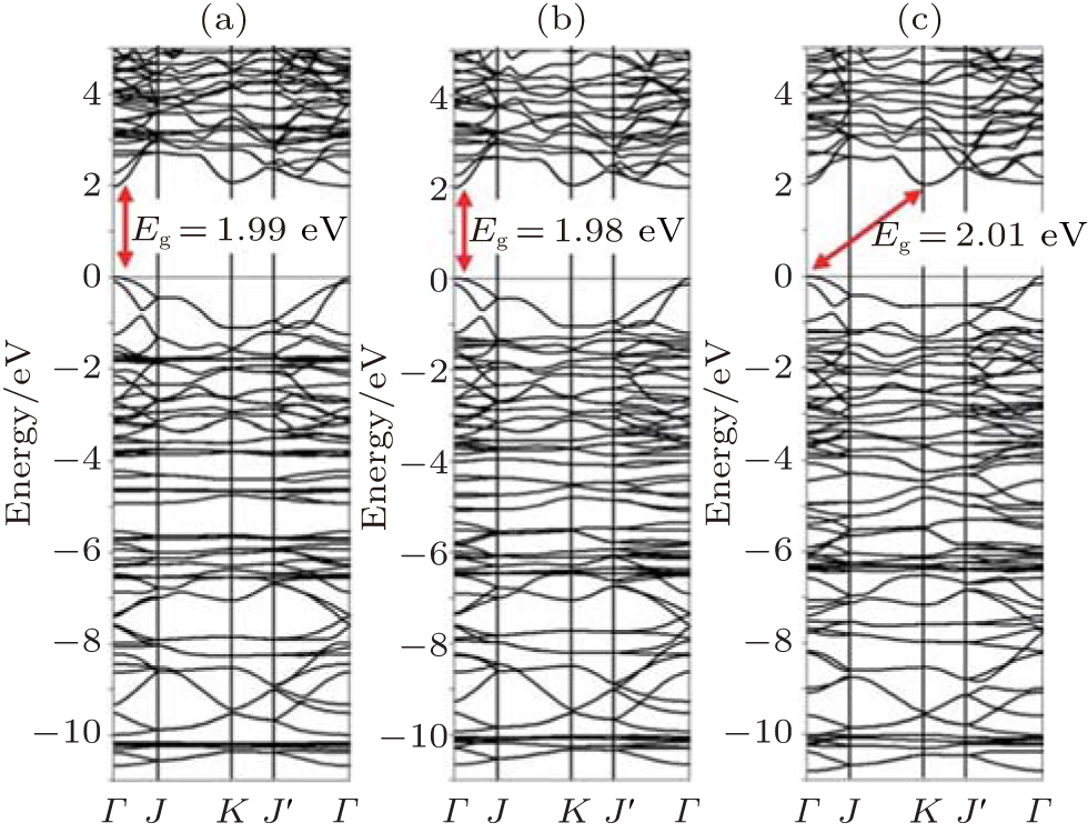 | Fig. 18. Band structures of phenylated silicene obtained by using the optB88 functional at the separation distances of (a) 27.64 Å (infinite), (b) 10.14 Å (minimum), and (c) 8.64 Å (compressed). The bandgap (Eg) is indicated by the arrow.[45] |
phenylated silicene nanosheets. At the minimum interfacial separation distance (10.14 Å ), phenylated silicene remained to be a direct-bandgap semiconductor with a smaller bandgap of 1.98 eV (Fig. 18(b)). When the separation distance of phenylated silicene sheets was compressed to be 8.64 Å , phenylated silicene became an indirect bandgap semiconductor with the bandgap of 2.01 eV (Fig. 18(c)). This suggested that the properties of phenylated silicene could be tuned by exerting compression stress.
Like what occurs to traditional silicon materials, the oxidation of silicene is of the great question during the fabrication of silicene-based devices. The formation of silicene oxides and the effect of oxidation on the electronic properties of silicene have been investigated experimentally and theoretically.
The oxidation of silicene with O2 dosing in an ultrahigh vacuum (UHV) environment is different from that upon exposure to air. We now review experiments on these two types of silicene oxidation.
Silicene exhibits strong resistance towards oxidation upon O2 exposure in an UHV environment.[48, 49] Molle et al. synthesized silicene on an Ag (111) substrate by molecular beam epitaxy (MBE).[49] Figure 19(a) shows that silicene has the superstructures of 
Friedlein et al. investigated the oxidation of silicene on the substrate of ZrB2 with O2 dosing in an UHV environment.[50] They also found that the scarce oxidation of silicene only started at a high dose (4500 L) of O2 as shown in Fig. 20(a). They studied the oxidation of silicene with different coverage of Al atoms. It was found that the Al coverage led to rather small changes in the Si 2p spectra (Fig. 20(b)). This indicated that the interaction between Al atoms and silicene was very weak. Upon exposure to O2, a broad Si 2p high-binding energy component located at ∼ 103 eV appeared, indicating that a major fraction of Si atoms was oxidized (Fig. 20(c)). Therefore, Al atoms could catalyze the oxidation of silicene with O2 dosing in an UHV environment.[50]
 | Fig. 19. (a) 35 nm× 35 nm STM topography of silicene on Ag (111) substrate. The STM topography illustrates the interplay of differently structured silicene domains. (b) Si 2p XPS spectra of silicene epitaxially grown on Ag (111). (c) Si 2p XPS spectra of silicene exposed to 1000-L O2.[49] |
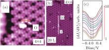
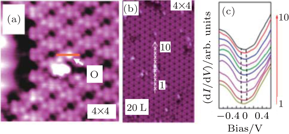
Figure 21 shows Du et al.’ s STM results on the oxidation of silicene. They found that an oxygen atom overbridged two adjacent Si atoms in silicene, leading to the formation of Si– O– Si bonds in silicene oxide (Fig. 21(a)).[46] They also studied the electronic properties of this type of so-called partially oxidized silicene by scanning tunneling spectroscopy (STS) differential conductance (dI/dV) measurements (Figs. 21(b) and 21(c)). It was found that the oxidation opened the bandgap of silicene by 0.11 eV– 0.18 eV, depending on the superstructures of silicene. Moreover, the bandgap of oxidized silicene was larger at oxygen sites and became smaller in the locations away from oxygen. The bandgap was the same within a lateral distance of 3 nm around an oxygen atom, implying that oxygen could affect the electronic structure of silicene in a relatively large area.[46]
 | Fig. 20. Si 2p XPS spectra of (a) pristine silicene before and after exposure to the O2 doses of 100 L and 4500 L, (b) silicene with the surface coverage of Al atoms ranging from x = 0 (pristine) to x = 0.38± 0.06, (c) silicene with the surface coverage of 0.38± 0.06 for Al atoms before and after exposure to the O2 doses of 100 L and 4500 L.[50] |
 | Fig. 21. (a) STM image of partially oxidized silicene in the 4× 4 structure, (b) STM image of the 4× 4 silicene exposed under an oxygen dose of 20 L. The arrowed line cutting across the oxygen atom represents the locations where the STS measurements are carried out, (c) the tunneling spectra (dI/dV curves) obtained along the line denoted in panel (b). The dashed lines in each STS result identify the bandgap.[46] |
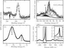
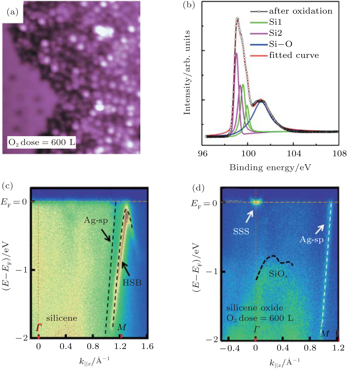
Xu et al. continued Du et al.’ s investigation by increasing the oxygen dose to 600 L.[51] As shown in Fig. 22(a), the increase of the concentration of O atoms transformed the original silicene into a disordered structure. Figure 22(b) shows that the Si– O peak at a binding energy of 101.6 eV clearly appeared after oxidation. The binding energy of the Si– O bond in oxidized silicene was lower than that in SiO2 (102.3 eV). This suggested that the charge states of Si in the silicene oxide were lower than + 4. Hence, silicene was only partially oxidized. They investigated the electronic properties of silicene before and after exposure to 600-L O2 by measuring the angle resolved photoemission spectroscopy (ARPES). Figure 22(c) shows that there existed a weak Ag sp-band, indicating that the Ag sp-band remained stable upon the deposition of silicene. The clear hybrid surface band (HSB) located at the k = 1.28 Å − 1 was attributed to the hybridization of Si and Ag orbitals. The HSB indicated the metallic property of silicene. Figure 22(d) shows that after oxidation the metallic HSB disappeared, suggesting that the hybridization between Si and Ag was broken due to the oxidation of silicene. In the meantime, the Shockley surface state (SSS) bands resulting from the surface states of free electrons at the Ag/vacuum interface appeared. Clearly, the silicene oxide did not cover the Ag (111) substrate entirely. It was important that an asymmetric band with the highest energy at ∼ − 0.6 eV was observed. This band was the valence band related to silicene oxide.[51] Therefore, it was concluded that silicene was oxidized into a semiconductor.
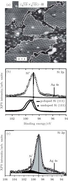
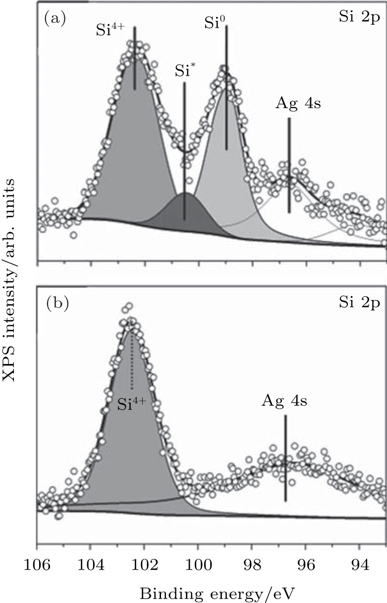
The oxidation of silicene upon exposure to air is very different from that under O2 exposure in ultra-high vacuum. Molle et al.’ s investigation showed that the oxidation of silicene started after 3 min exposure to air.[49] The Si 2p XPS spectrum of silicene after 3-min exposure to air could be divided into three contributions as shown in Fig. 23(a). The peak related to the pristine silicene (Si) remained, indicating the existence of Si– Si bonds after 3-min exposure to air. The major Si– O component indicated by the binding energy of 102.3 eV was related to the SiO2-like chemisorption (Si4+ peak). The third peak (Si* ) was associated with the bonding of sub-oxide species with lower valence states of Si. Therefore, silicene after 3-min exposure to air was partially oxidized. However, after 1-day exposure to air, silicene was fully oxidized, because the Si 2p XPS spectrum could be totally attributed to the SiO2-like chemisorption (Fig. 23(b)).
 | Fig. 22. (a) STM image of the 4× 4 silicene oxidized under oxygen dose of 600 L. (b) Si 2p core level XPS spectra of 4× 4 silicene on Ag (111) after oxidation. Energy versus k dispersion measured by ARPES for the 4× 4 silicene before (c) and after (d) oxidation.[51] |
 | Fig. 23. Si 2p XPS spectra of silicene (a) after 3-min exposure to air and (b) silicene after 1-day exposure to air.[49] |
Molle et al. further studied the deposition of Al and Al2O3 layers on the top of silicene for hindering the oxidation of silicene in air.[49] It was found that the Si 2p line shifted to lower binding energy after the deposition of 4-nm Al-capping layer, which was related to the extra charge exchange between the Al and Si orbitals (Fig. 24(a)). Molle et al. investigated the oxidation of 7-nm-thick Al capped silicene upon air exposure. After oxidation, the Al 2p line had two components (Fig. 24(b)). The Al* peak was related to partial Al oxidation at the surface while the Al peak was related to original Al– Al bonding at the bottom of the capping layer. The preservation of a pure Al layer at the bottom of the capping layer can prevent the underlying silicene from oxidizing. Molle et al. also studied the effect of the direct deposition of Al2O3 on the oxidation of silicene. Figure 24(c) shows a four-component XPS line for Al2O3 capped silicene on Ag (111). The Ag 4s related peak was associated with the Ag (111) substrate. The Si peak was related to the Si– Si bonding in silicene. The Si* peak at the binding energy of 101.6 eV was related to the partial oxidation of silicene. The Al2O3 -related peak was at the binding energy of 103.3 eV. Molle et al. also investigated the oxidation of Al2O3-capped silicene upon air exposure by Raman spectroscopy. As shown in Fig. 24(d), the narrow peak at 516 cm− 1 that was related to silicene indicated that deposition of Al2O3 layer prevented silicene from oxidizing.
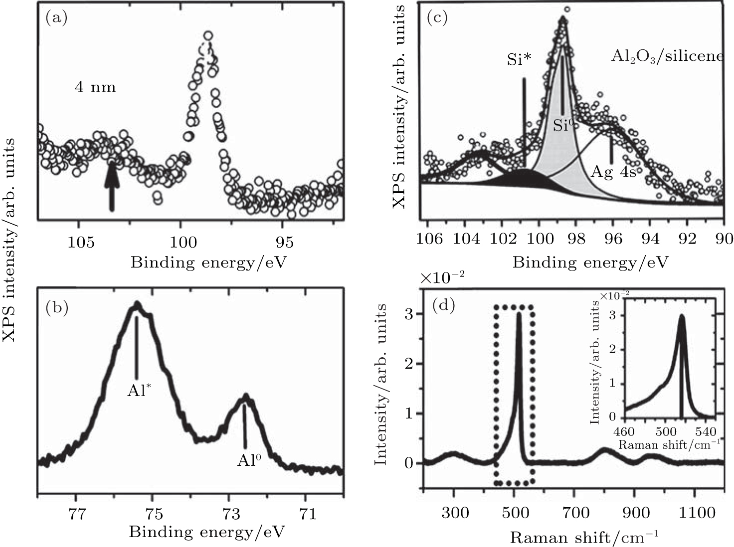 | Fig. 24. (a) Si 2p XPS line of as-synthesized 4-nm-thick Al-capped silicene, (b) Al 2p XPS line of the 7-nm-thick Al-capped silicene after exposure to air, (c) Si 2p XPS line of the as-synthesized Al2O3-capped silicene, and (d) Raman spectrum of the Al2O3-capped silicene exposed to air.[49] |
De Padova et al. showed that multilayer silicene (up to 43 layers) exhibited a small amount of surface oxidation after 1-day exposure to air. They claimed that the oxidized region at the surface served as an encapsulation layer for the rest of the silicene film.[47]
Liu et al. have studied the adsorption and dissociation of oxygen (O2) molecules on silicene by first-principles calculation.[29] Their results showed that O2 molecules could be easily adsorbed at the silicene surface and dissociated into O atoms without overcoming any energy barrier. The dissociated O atoms were difficult to migrate on and desorb from the silicene surface (Fig. 25) Therefore, silicene could be easily oxidized. They proposed that hydrogenation of silicene would hinder the oxidation of silicene by increasing the energy barrier of O2 molecule adsorption and dissociation.[29]
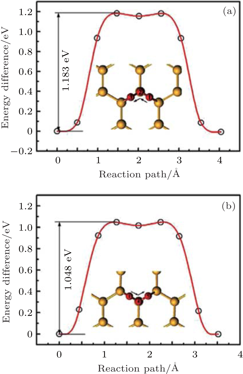 | Fig. 25. Energy difference of an O atom migrating along the pathways (a) 1-2-3 and (b) 1-4-5 on the silicene surface. (b) The insets of figures show the optimized migration pathways of 1-2-3 (a) and 1-4-5 (b).[29] |
Wang and Ding investigated the mechanical and electronic properties of oxidized silicene with the stoichiometric ratio of Si:O= 1:1.[52] The Poisson ratios of these silicene oxides were negative, indicating that these silicene oxides exhibited unconventional auxetic behavior and thus could have obvious elastic characteristics. It was found that the silicene oxide was a direct-bandgap semiconductor with the bandgap of 0.18 eV. Meanwhile, the carrier mobility of the silicene oxide was on the order of magnitude of 104 cm2· V− 1· s− 1.[52]
Wang et al. have systematically investigated the formation, structures, and electronic properties of oxidized silicene.[53] In their investigation, the oxidation of silicene was the reaction between silicene and oxygen (O) atoms or hydroxyl groups (OH). The bonding configurations of atomic O included quasi-in-plane bridging O (Oqb), double bridging O (Odb), overbridging O atoms located at either both sides 

Fully oxidized silicene was obtained by incorporating Oqb with other types of O or OH configurations. It was demonstrated that all the silicene oxides might be formed in the point of view of thermodynamics. The Ef per atom of oxygen in a silicene oxide was calculated by using Ef = (Et− Es− NOμ O2/2− NOHμ OH)/NO, where Et was the total energy of the SO. Es was the total energy of silicene. NO and NOH were the numbers of O atoms and OH radical groups, respectively. μ O2 and μ OH were the chemical potentials of O2 molecules and OH radical groups, respectively. The change of Ef with respect to Δ μ OH (the difference between μ OH in the oxidation system of silicene and that in water) for each silicene oxide was shown in Fig. 26. For the silicene oxides induced by the partial oxidation with O atoms (e. g., in the atmosphere of oxygen gas), Ef increased in the order of 


Wang et al. have also studied the electronic properties of oxidized silicene.[51] Their results showed that oxidation could transform silicene from semimetal to metal, semiconductor and insulator by controlling the configurations of O and OH incorporated into silicene. For semiconducting silicene oxides, the carrier motilities are less than 100 cm2· V− 1· s− 1.[53] The prediction of the electronic properties of silicene oxides opened an avenue to tailoring the properties of silicene through oxidation. Nevertheless, excellent control on the oxidation conditions needs to be exerted to obtain specific silicene oxides with desired electronic properties.
Like the critical role of doping in traditional semiconductor technologies, it is believed that new technologies based on silicene may also depend on doping. For silicene, it is possible to tune the doping states by changing external fields.[5– 7] Replacing Si atoms in silicene with foreign atoms (e.g., B, P, N, Al, Cr, etc.) offers the possibility of tuning the structural, electronic, optical, and magnetic properties of silicene. It should be noted that in this paper we define doping as replacing Si atoms in silicene with foreign atoms. Researches on the adsorption of foreign atoms on silicene are not included.[54– 56] In this section we will deal with the doping of silicene with both non-metallic and metallic atoms.
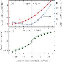
Cheng et al. studied the effects of carrier concentration on the lattice structure, electronic structure, phonon spectrum, and electron– phonon coupling of silicene by first-principles calculations.[57] They found that the lattice parameters of silicene were sensitive to the carrier concentration. As shown in Fig. 27(a), the lattice parameter (α ) of p (n)-type silicene was smaller (larger) than that of the undoped silicene. This indicated that the lattice of silicene expanded (shrunk) when electrons were added (extracted). The buckling distance (Δ ) of doped silicene was larger than that of undoped silicene except for the case for p-type silicene with low carrier concentrations (Fig. 27(a)).
 | Fig. 27. Variations of (a) the lattice parameter (σ ) and buckling distance (Δ ), (b) the Fermi energy with carrier concentration (σ ).[57] |
The lattice parameter and buckling distance were more sensitive to the carrier concentration for n-type doping than for p-type doping. The Dirac cone of silicene mainly results from the 3pz orbitals of Si. The bands located at 1 eV above and below the Fermi level mainly originate from the 3s and 3px, y orbitals of Si. Hence, it was predicted that doping mainly affected the occupation of the π and π * bands. Cheng et al. demonstrated that the relationship between the carrier concentration (σ ) and the Fermi energy (EF) is 
Heavily doped silicene has also been studied. Sivek et al. have investigated the doping of silicene by using B, N, and P atoms with a dopant concentration of 3.2%, [58] which was achieved by replacing one Si atom in a 4× 4 silicene supercell with a B, N or P atom. Their molecular dynamics calculations indicated that the resulting structures were all stable up to at least 500 K. Figure 28 shows the band structures and decomposed DOS of silicene doped with B, N, and P atoms, obtained with DFT calculations. It was shown that the Dirac cone of silicene was preserved after the doping of B and P atoms. The Dirac cones originating from the pz orbitals of Si shifted above and below the Fermi level for B- and P-doped silicene, respectively. The shifted valance band or conduction band crossed the Fermi level for B- or P-doped silicene. Therefore, B- and P-doped silicene were metals. B and P mainly affect the deep bands of doped silicene (Figs. 28(a) and 28(b)). Silicene doped with N turned out to be metallic with a band crossing the Fermi level and relative large DOS near the Fermi level. The p orbitals and s orbitals of N and Si both contributed to the bands of N-doped silicene (Fig. 28(c)). Interestingly, N-doped silicene became ferromagnetic with a net magnetic moment of 0.9 μ B.[58]
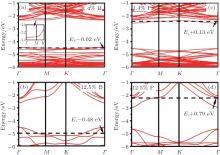
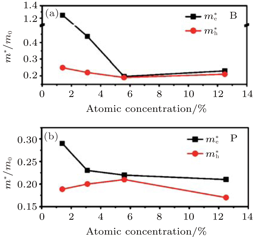
Pi et al. investigated the doping of hydrogenated silicene by using B and P with the dopant concentrations ranging from 1.4% to 12.5% in the framework of DFT.[59] They found that doped hydrogenated silicene structures became direct-bandgap semiconductors with the VBM and CBM both located at the Γ point. As shown in Fig. 29, the Fermi level entered the valence (conduction) band for B (P)-doped hydrogenated silicene even when the concentration of B (P) was 1.4%, indicating that hydrogenated silicene was heavily doped even for the lowest dopant concentration of 1.4% in their work.[59] As the dopant concentration increased from 1.4% to 12.5%, the difference in energy between the Fermi level and the VBM (CBM) of B (P)-doped hydrogenated silicene became larger (i.e., 0.02 eV– 0.48 eV for B-doped hydrogenated % silicene, 0.13 eV– 0.79 eV for P-doped hydrogenated silicene). The difference in energy between the direct bandgap and the indirect bandgap of B-doped hydrogenated silicene was smaller than that of P-doped silicene. Therefore, P doping more severely modified the band structure of hydrogenated silicene than B doping.
 | Fig. 28. Electronic band structures and decomposed densities of states (DOSs) for silicene doped with (a) B, (b) P or (c) N. The Fermi level is located at the zero-energy level.[58] |
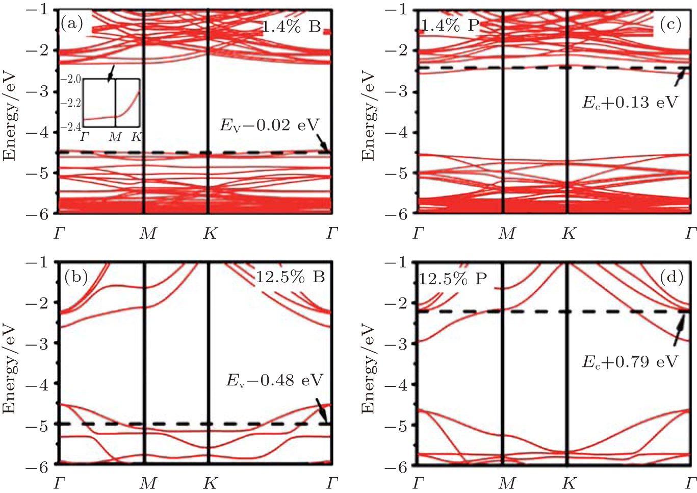 | Fig. 29. Band structures of H-silicene doped with B at the concentrations of (a) 1.4%, (b) 12.5% and H-silicene doped with P at the concentrations of (c) 1.4%, (d) 12.5%. The Fermi level is indicated by a horizontal dashed line.[59] |
Pi et al. have also calculated the effective mass (m* ) of holes (electrons) at the VBM (CBM) of hydrogenated silicene doped with B or P.[59] They found the largest carrier mobility could be achieved when the concentration of B was 5.6%. This might be understood by considering the smallest 

Sivek et al. have investigated the electronic property of Al-doped silicene with the concentration of 3.2%.[58] Their molecular dynamics calculations indicated that Al-doped silicene was stable up to at least 500 K. The effect of Al doping on the electronic properties of silicene was similar to that of B doping. Al-doped silicene exhibited metallic properties. The Dirac cone derived from the pz orbitals of Si atoms shifted to above the Fermi level. Doped Al atoms mainly affected the deep bands of Al-doped silicene.[58]
Hussain et al. studied the stability, electronic structure, and hydrogen storage capacity of Mg-doped hydrogenated silicene.[28] The structure of Mg-doped hydrogenated silicene was stable in the point of view of thermodynamics. Exerting biaxial symmetric strain could increase the binding energy of Mg atoms and enhance the stability of Mg-doped H-silicene. Mg-doping changed hydrogenated silicene from a semiconductor to a metal. The electronegativity of Si is much higher than that of Mg, leading to charge transfer from Mg atoms to Si atoms. The resulting positive charges on each Mg atom can accumulate up to six H2 molecules, giving rise to an H2 storage capacity of 7.95%.[28] Therefore, Mg-doped hydrogenated silicene may be an ideal H2 storage material.
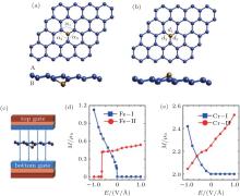
Zheng et al. have studied the magnetoelectric (ME) properties of silicene doped with Fe and Cr atoms by first-principles calculations.[60] They replaced one Si atom in a 4× 4 silicene supercell with an Fe or Cr atom. The resulting dopant concentration was 3.2%. There were two different structures with different changes of magnetism under external electric field. Silicene has a buckled structure with two sublattices denoted as the sublattices A and B. Upon doping, an Fe or Cr atom can substitute an Si atom in the sublattice B (A), resulting in the X– I (X– II) structure as shown in Figs. 31(a) and 31(b). Figure 31(c) shows that a perpendicular field was applied to the doped silicene to investigate its magnetoelectric properties. Figure 31(d) illustrates that the magnetoelectric response of the Fe– I structure critically depended on the direction of the electric field. When the external electric field (Eext) was positive, the magnetic moment (M) of the Fe– I structure was zero. When Eext was negative, the magnetic moment of the Fe– I structure increased linearly with the increase of the absolute value of Eext. A clear switching effect was found in the Fe– II structure. A sharp jump of the magnetic moment from 0.41 μ B to 0 occurred when Eext changed from − 0.65 V/Å to − 0.66 V/Å . For the Cr– I structure, the magnetic moment was ∼ 2 μ B when Eext was positive. When Eext was negative, the magnetic moment decreased approximately linearly with the increase of the absolute value of Eext. For the Cr– II structure, the magnetic moment increased nearly linearly when Eext increased from -1 V/Å to 1 V/Å (Fig. 31(e)). It was found that the different magnetoelectric responses of Fe- or Cr-doped silicene were related to the electronic states around the Fermi level.[60] The interesting magnetoelectric responses of Fe- or Cr-doped silicene has potential applications in magnetoelectric diodes and magnetoelectric devices with high speed response.
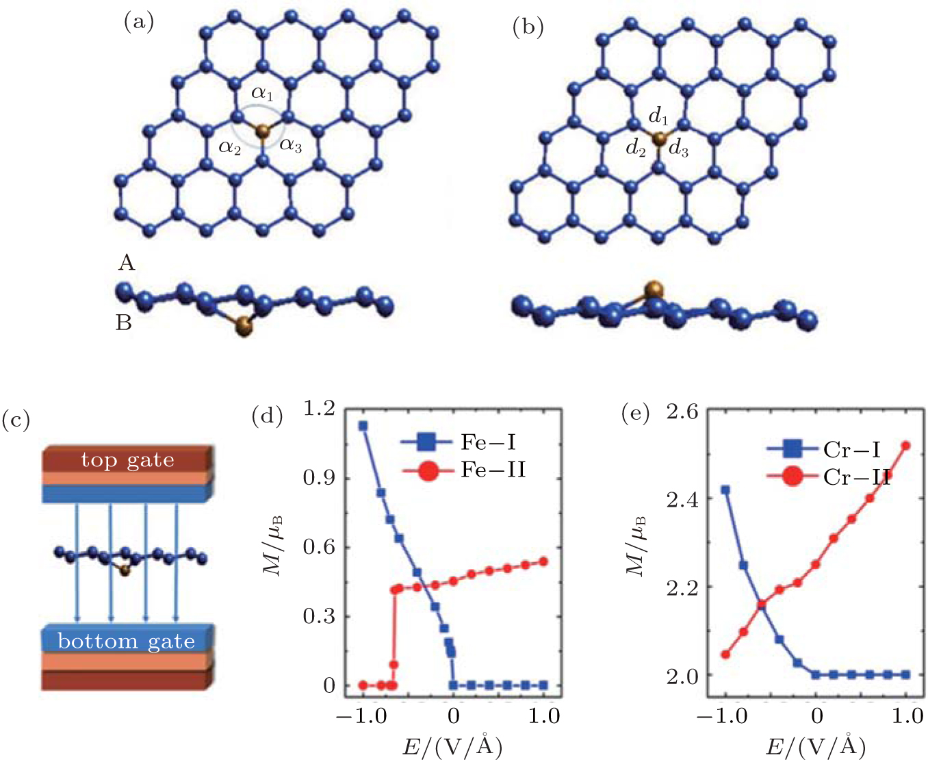 | Fig. 31. (a) Optimized structure of Fe– I in a 4× 4 supercell with the Fe atom below the silicene plane, (b) the optimized structure of Fe– II in a 4× 4 supercell with the Fe atom above the silicene plane, (c) the direction of the external electric field during the simulation of the magnetoelectric properties for doped silicene, (d) the magnetic moment of Fe-doped silicene for the 4× 4 supercell as a function of the external electric field, and (e) the magnetic moment of Cr-doped silicene for the 4× 4 supercell as a function of the external electric field.[57] |
Formation of 2D hybrids provides an additional degree of freedom for the materials design of silicene. Since Si, C, and Ge are all group IV elements, they may readily form hybrids in principle. Graphene and germanene have been synthesized. It is reasonable to expect the formation of silicene– graphene hybrids and silicene– germanene hybrids. To date, both the silicene– graphene hybrids and silicene– germanene hybrids have been theoretically investigated.
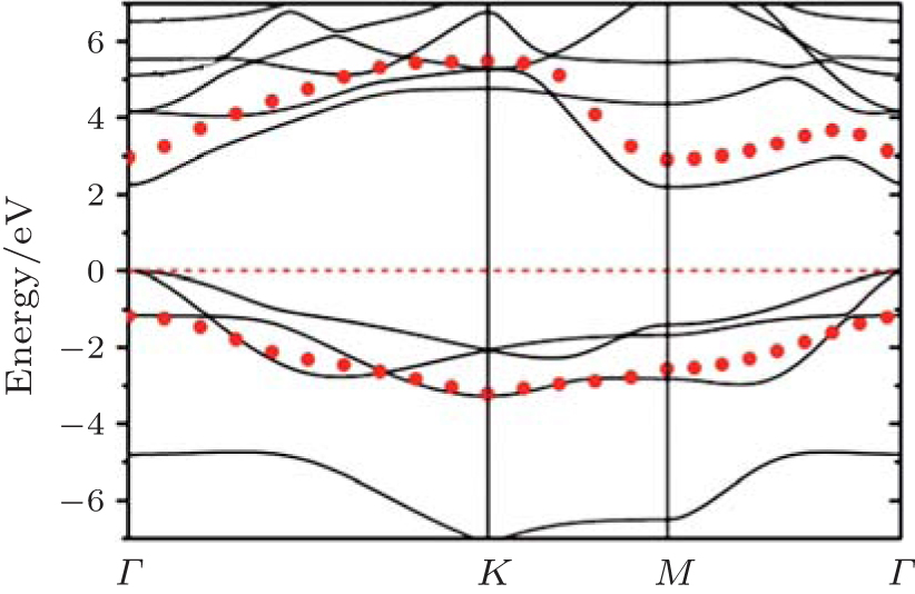
Figure 32 shows the optimized structure of a silicene– graphene (SC) hybrid with Si/C = 1. Drissi et al.’ s LDA– DFT calculations indicated that this type of SC hybrid was stable with a planar hexagonal lattice. The Si– C bond length was 1.78 Å . The Si– C– Si/C– Si– C bond angles (∠ (Si– C– Si)/∠ (C– Si– C) were 120° .[61] They found that the SC hybrid was a direct-bandgap semiconductor with a bandgap of 2.4 eV.[61]
Since DFT calculations underestimate the bandgap energies of semiconductors, Drissi and Ramadan then calculated the band structure of the SC hybrid with the GW approximation to include the quasiparticle corrections.[62] As shown in Fig. 33(a), the GW approximation calculation indicated that the SC hybrid was a direct bandgap semiconductor. The VBM and CBM were both located at the K point. The bandgap was 3.48 eV. They also calculated the optical absorption spectra of the SC hybrid by using LDA– RPA, GW– RPA (with quasiparticle corrections), and GW– BSE (with quasiparticle corrections and electron– hole interactions). The shapes of the absorption spectra calculated by using LDA– RPA and GW– RPA methods were quite similar. The GW– RPA only shifted the absorption spectra to high energies. After taking the electron– hole interactions into account, Drissi and Ramadan found that the first absorption peak which corresponded to the optically active excitonic state emerged at 2.67 eV (Fig. 33(b)). The exciton was mainly related to the vertical transition of electrons at the K-point between the π state in the VBM and the π * state in the CBM.[62]
 | Fig. 33. (a) Band structures and (b) optical absorption spectra of the silicene– graphene hybrid calculated by different calculating methods.[62] |
 | Fig. 34. (a) Optimized structures of the CSi3 hybrid with both top and side views and (b) orbital-resolved band structure of the CSi3 hybrid.[64] |
Zhang et al.’ s calculations revealed that the SC hybrid exhibited an excellent catalytic activity for oxygen reduction reaction without CO poisoning.[63] The SC hybrid in alkaline medium had better catalytic activity than conventional Pt (111) surface. Therefore, the SC hybrid is likely to be used as a metal-free catalyst for oxygen reduction reaction in fuel cells.
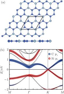
Ding and Wang investigated the geometrical and electric properties of the SC hybrid with the stoichiometric ratio of Si:C = 3:1, which was shown in Fig. 34(a).[64] They found that the CSi3 hybrid was also stable in a planar hexagonal lattice with an Si– C (Si– Si) bond length of 1.81 Å (2.26 Å ). Figure 34(b) shows the band structure of the CSi3 hybrid. It is clear that the CSi3 hybrid is semi-metallic. Its CBM mainly originates from the C pz orbital, while its VBM is mainly related to the Si pz orbital.[64] This interesting phenomenon provides a peculiar example, which shows that orbitals from different elements can also form linear π and π * bands around the Dirac cone.
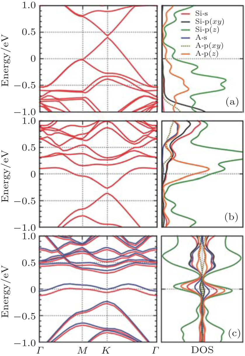
The optimized structure of silicene– germanene (SG) hybrid is quite similar to that of the SC hybrid. However, the SG hybrid has a buckled structure, with an Si– Ge bond length of 2.38 Å and a buckling distance of 0.60 Å (Fig. 35(a)). The band structure of the SG hybrid indicates that it is a semimetal with the top of the valence band and the bottom of the conduction band linearly crossing at the Fermi level (Fig. 35(b)).[65]
 | Fig. 35. (a) Optimized structure of the silicene– germanene hybrid with both top and side view. Si and Ge atoms are denoted by yellow and green balls, respectively. (b) The band structure (left) and the partial DOS (right) of the silicene– germanene hybrid.[65] |
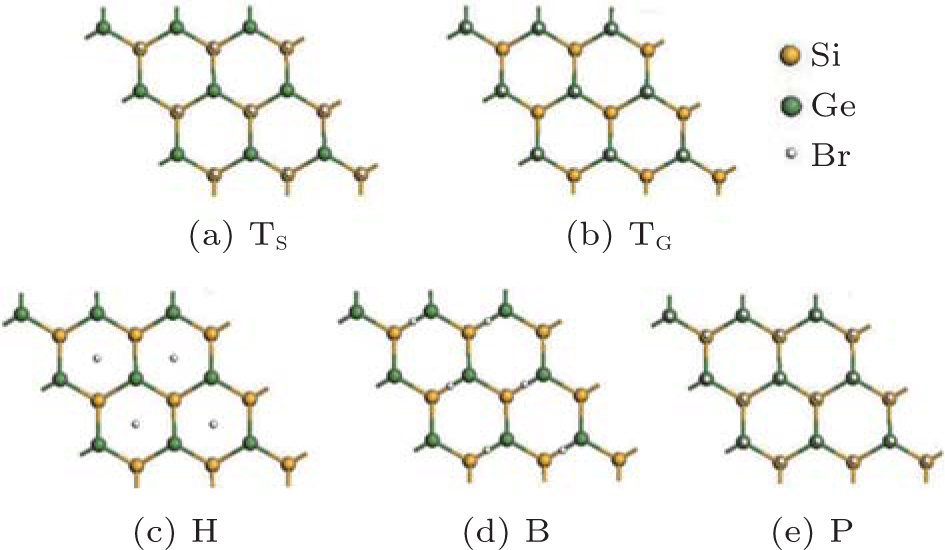
Zhang et al. have also investigated the properties of brominated SG hybrids.[65] Bromine atoms could adsorb on or passivate the SG hybrid at the sites of TS, TG, B, and H (Fig. 35(a)). Figure 36 shows the resulting structures of brominated SG hybrids, which are denoted as TS, TG, B, and H. Structure P in which Br atoms passivate the nearest neighbored Si and Ge atoms is also considered (Fig. 36). By comparing the binding energies of brominated SG hybrids with different configurations, Zhang et al.[65] found that the TS structure was most stable. The bond lengths of Si– Ge and Si– Br in the brominated SG hybrid with the TS configuration were 2.43 Å and 2.02 Å , respectively. For the brominated SG hybrid with the TS structure the spin-up channel had a bandgap of 1.73 eV, while the spin-down channel was characteristic of metallic bands. Upon bromination, Br atoms and Si atoms formed strong σ bonds, leaving Ge atoms unsaturated. The unpaired pz electrons of unsaturated Ge atoms resulted in spin polarization, which caused a net magnetic moment of 1.0 μ B. From the spin-density distributions of the brominated SG hybrid with the TS structure, it was inferred that the total magnetic moment mainly resulted from unpaired Ge atoms.
The chemical modification of silicene is an important issue in the development of silicene. Theoretical researchers have done a lot of studies on the geometrical, electronic, optical, and magnetic properties of chemically modified silicene in the past few years. The successful synthesis of silicene has accelerated the experimental work on the chemical modification of silicene.[79– 84] In the present work, we have reviewed the effects of hydrogenation, halogenation, organic surface modification, oxidation, doping, and formation of 2D hybrids on the various properties of silicene. It has been theoretically demonstrated that chemical modification offers the possibility of tuning the properties of silicene by passivating or substituting Si atoms in silicene. Metals, semimetals, semiconductors, and insulators may be produced from the single material of silicene only by means of chemical modification. However, experimental work on the chemical modification of silicene remains rather limited. There are only a few experiments on the organic surface modification, oxidation, and hydrogenation of silicene.
In order to facilitate the experiments on the chemical modification of silicene, further theoretical investigation needs to be carried out to search for novel properties enabled by the chemical modification of silicene and guide the design of rational routes for the chemical modification of silicene. Moreover, the interaction between chemically modified silicene layers deserves careful investigation. The stacking of chemically modified silicene may lead to novel properties. One of the most important goals of chemical modification is to open and tune the bandgap of silicene, and thus facilitating the applications of chemically modified silicene in various device structures. In this context, simulation on silicene-based devices is highly desired. It is clear that the modulating of the properties of silicene by chemical modification depends on the accurate control of the bonding configurations. Excellent control of the chemical modification processes must be exerted to obtain specific chemically modified silicene with desired properties.
| 1 |
|
| 2 |
|
| 3 |
|
| 4 |
|
| 5 |
|
| 6 |
|
| 7 |
|
| 8 |
|
| 9 |
|
| 10 |
|
| 11 |
|
| 12 |
|
| 13 |
|
| 14 |
|
| 15 |
|
| 16 |
|
| 17 |
|
| 18 |
|
| 19 |
|
| 20 |
|
| 21 |
|
| 22 |
|
| 23 |
|
| 24 |
|
| 25 |
|
| 26 |
|
| 27 |
|
| 28 |
|
| 29 |
|
| 30 |
|
| 31 |
|
| 32 |
|
| 33 |
|
| 34 |
|
| 35 |
|
| 36 |
|
| 37 |
|
| 38 |
|
| 39 |
|
| 40 |
|
| 41 |
|
| 42 |
|
| 43 |
|
| 44 |
|
| 45 |
|
| 46 |
|
| 47 |
|
| 48 |
|
| 49 |
|
| 50 |
|
| 51 |
|
| 52 |
|
| 53 |
|
| 54 |
|
| 55 |
|
| 56 |
|
| 57 |
|
| 58 |
|
| 59 |
|
| 60 |
|
| 61 |
|
| 62 |
|
| 63 |
|
| 64 |
|
| 65 |
|
| 66 |
|
| 67 |
|
| 68 |
|
| 69 |
|
| 70 |
|
| 71 |
|
| 72 |
|
| 73 |
|
| 74 |
|
| 75 |
|
| 76 |
|
| 77 |
|
| 78 |
|
| 79 |
|
| 80 |
|
| 81 |
|
| 82 |
|
| 83 |
|
| 84 |
|