


Bending-induced phase transition in monolayer black phosphorus
[Pan Dou-Xing†a), c)  , Wang Tzu-Chiang
a) , Guo Wan-Linb) ]
, Wang Tzu-Chiang|
|


†Corresponding author. E-mail: pandx@lnm.imech.ac.cn
*Project supported by the National Natural Science Foundation of China (Grant Nos. 11021262, 11172303, and 11132011) and the National Basic Research Program of China (Grant No.2012CB937500).
Bending-induced phase transition in monolayer black phosphorus is investigated through first principles calculations. By wrapping the layer into nanotubes along armchair and zigzag directions with different curvatures, it is found that phase transitions of the tubes occur when radius of curvature is smaller than 5 Å in bending along the zigzag direction, while the tubes remain stable along the armchair direction. Small zigzag tubes with odd numbered monolayer unit cells tend to transfer toward armchair-like phases, but the tubes with even numbered monolayer unit cells transfer into new complex bonding structures. The mechanism for the bending-induced phase transition is revealed by the comprehensive analyses of the bending strain energies, electron density distributions, and band structures. The results show significant anisotropic bending stability of black phosphorus and should be helpful for its mechanical cleavage fabrication in large size.
Black phosphorus (BP) has been extensively studied since the 1980s, and its few-layered structures received wide attention last year[1– 3] as a novel two-dimensional (2D) functional material with high drain current modulation and charge-carrier mobility, promising for thin-film electronics, infrared optoelectronics and novel devices where anisotropic properties are desirable. Since then, mono-layered BP has been successfully fabricated by mechanical cleavage and subsequent Ar+ plasma thinning process.[4] Unlike graphene, large monolayer BP has not been obtained yet by mechanical exfoliation, which is mainly due to its distinct brittleness under bending load.[1– 4]
On the other hand, phase transition is one of the most fundamental phenomena and an important issue in material science and applied physics. For bulk BP, pressure-induced phase transition has been extensively studied.[5– 9] Under large debending strain, phase transitions in different materials have been widely observed, [10– 13] especially the tension-induced phase transition of mono-layered molybdenum disulphide.[13] However, the bending-induced phase transition in monolayer BP has never been reported.
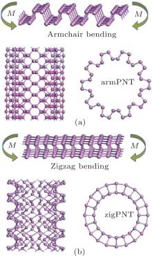
In this report, bending behaviors of BP are investigated through first principles calculations of single-walled BP nanotubes[14] with different curvatures. Two typical bending modes are simulated, by wrapping the BP monolayer into nanotubes along the armchair and zigzag directions (the corresponding tubes are defined as armPNTs and zigPNTs as shown in Fig. 2). It is interesting that phase transitions of the zigPNTs occur when radius of curvature is smaller than 5 Å in bending along zigzag direction, while all the armPNTs remain stable. The results suggest that mechanical exfoliation along the armchair direction may lead to larger BP monolayer.
All the calculations including ab initio molecular dynamics simulations are carried out within the framework of density functional theory (DFT)[15] implemented in the Vienna ab initio simulation package (VASP).[16, 17] The generalized gradient approximation in the form of the Perdew– Burke– Ernzerhof exchange– correlation functional[18] and the projector-augmented wave potentials are employed.[19– 21]
The energy convergence criterion for electronic iterations is set to be 10− 4 eV and the non-spin-polarized geometric structures are relaxed until the force on each atom is less than 0.01 eV/Å . The kinetic energy cutoff for the plane wave basis set is adopted to be 450 eV which guarantees that the absolute energy converges to around 2 meV.
The reciprocal space for the unit cell of BP and the corresponding nanotubes are meshed at 14× 10× 1 and 1× 1× 12 using Monkhorst Pack method centered at Γ point, respectively. A vacuum space of at least 20 Å is included in the unit cell to prevent the interaction between the cell and its image resulting from the periodic boundary condition.
The initial structure of the BP monolayer is obtained from bulk BP, [22, 23] which has a puckered honeycomb structure with each phosphorus atom covalently bonded with three adjacent atoms. The relaxed lattice constants are a1 = 4. 620 Å , a2 = 3.299 Å , and the thickness is h = 2.104 Å as shown in Fig. 1.
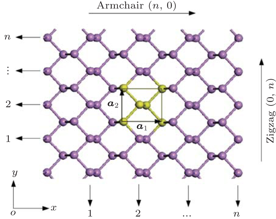 | Fig. 1. Structure of 2D puckered honeycomb BP. The yellow part indicates a unit cell and lattice vectors a1 and a2 along armchair(n, 0) and zigzag(0, n) directions, respectively. |
In this paper, the Born– Oppenheimer molecular dynamics (BOMD)[24, 25] simulations are performed for DFT-based molecular dynamics simulations. The supercell is at least three times the unit cell and the energy cutoff is set by PREC, = low. The time step is 1 fs and each independent BOMD simulation lasts 10 ps, with the micro-canonical ensemble adopted in the intermediate period.
The bending strain energy Eb can be considered as the energy of wrapping the BP layer into a nanotube and defined as

where N and n are the numbers of atoms and sheet unit cells in a nanotube unit cell, respectively; Es and Ent denote the free energies of a unit cell in the BP layer and the corresponding nanotube, respectively. Figure 2 shows snapshots of BP wrapped from its initial planar layer into tubes along the armchair direction (armchair bending) and zigzag direction (zigzag bending), respectively.
 | Fig. 2. Structures of BP in bent states. Bending moment M is perpendicular to (a) armchair direction (armchair bending) and (b) zigzag direction (zigzag bending). ArmPNT means the armchair single-walled phosphorus nanotube, and zigPNT the zigzag one. |
The radius of curvature is first chosen as an independent reference variable to facilitate the discussion, which is defined as beginequation
and r > 2.1 Å is taken for the two typical bending modes to guarantee that the initial geometric structures are in circular shape. Changes of bending strain energy with radius of curvature are shown in Fig. 3.
 | Fig. 3. Bending strain energies changing with radius of curvature for BP bent into nanotubes. (a) The curve of bending strain energy (in pink) in zigzag bending induced phase transition zone (PT zone) becomes significantly lower than the curve without phase transitions (in blue). For tubes with radius of curvature larger than the critical value rcr, no bending-induced phase transition (NPT zone) appears. (b) Comparison of bending strain energies of armchair and zigzag tubes between before and after the phase transition. Blue diamonds and circles indicate armPNT and zigPNT before phase transition, and pink pentagrams indicate phase transition phosphorus nanotube (zptPNT) under zigzag bending. |
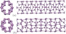
Figure 3(a) shows that for zigPNTs smaller than zigPNT(0, 10), the bending strain energy curve presents a large bifurcation and a new branch with much lower energies. Figure 3(b) shows a robust hyperbolic law for armchair bending, or armPNTs, even down to armPNT(4, 0) at a radius of 3 Å . This indicates that bending-induced buckling occurs only due to large curvature along the zigzag direction, which has been in detail analyzed in the light of continuum elasticity theory in our previous work.[26] It is surprising that the zigPNTs with small radius of curvature transfer into zptPNTs of interesting structural phases (see Fig. 5) with significantly lower energy. Recently, Guan et al.[27] presented a paradigm in constructing very stable faceted nanotube and fullerene structures by laterally joining nanoribbons or patches of different planar phosphorene phases, so it is necessary to further discuss the zptPNTs.
In order to examine thermal stabilities of zptPNTs, especially the smallest zptPNT(0, 5), the BOMD simulations are also carried out. As shown in Fig. 4, the structure of zptPNT(0, 5) is still intact at 500 K after 10 ps of simulation but shows some deformations. At low temperature of 50 K, the overall structure of zptPNT(0, 5) is well kept after 10-ps simulation. Our BOMD simulation on zptPNT(0, 7) also shows a similar stability and the detailed results are presented in Appendix A, although the zptPNT (0, 5) is stabler. As shown in the appendixes, the stabilities of other zptPNTs are further investigated by using different methods. The phonon dispersions of zptPNT(0, 4) and zptPNT(0, 8) are calculated and presented in Appendix B, which shows no negative phonon spectrum. What is more, we check the stability of the zptPNT(0, 9) by post-hydrogenation passivation (see Appendix C for the details).
 | Fig. 4. DFT-based BOMD simulations at 10 ps for the zptPNT (0, 5) [top view on the left and side view on the right] controlled at (a) low temperature of 50 K and (b) 500 K. |
In Fig. 3(a), the bending-induced phase transition zone (PT zone) under zigzag bending is separated from the non-phase transition zone (NPT zone) by a critical radius of curvature rcr = 5.25 Å of zigPNT(0, 10). Although zigPNTs still exist in the PT zone as shown by the blue curve in the figure, they are metastable by comparison with the corresponding zptPNTs, which have significantly lower energies. However, no metastable zigPNT smaller than zigPNT(0, 6) (with radius of 3.15 Å ) exists.
From the isosurface electronic density diagram of zptPNTs in Fig. 5, three obvious features can be observed which are helpful for understanding the bending-induced phase transition.
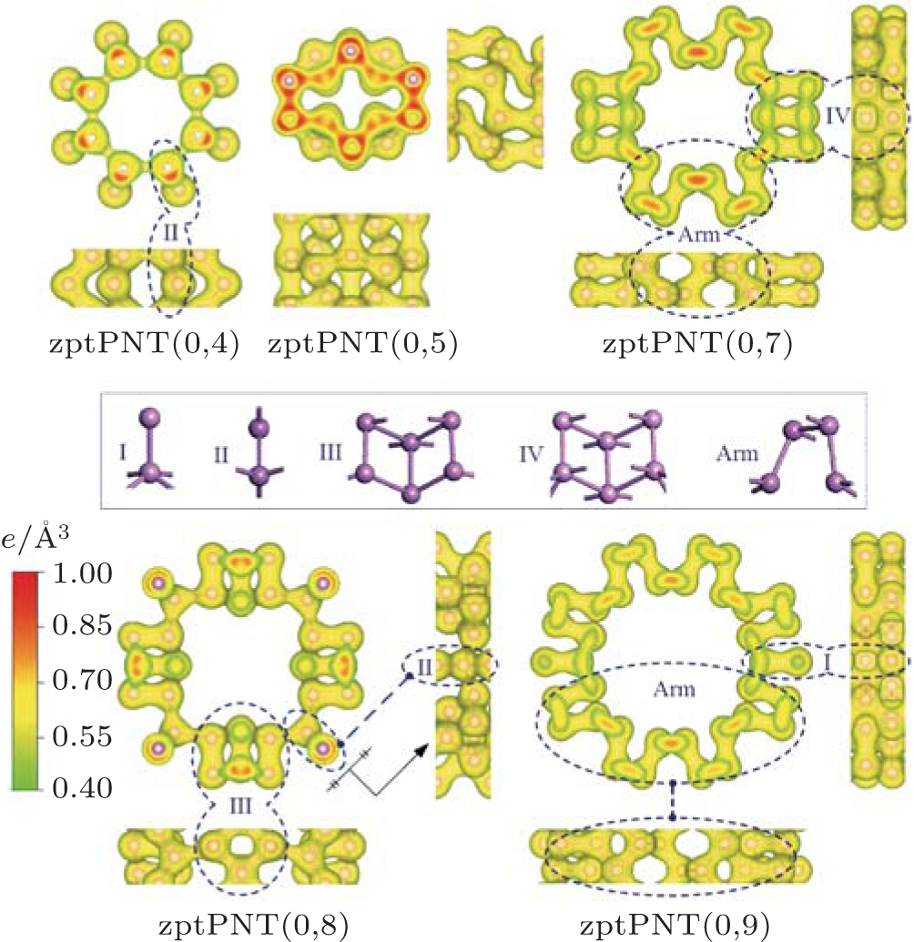 | Fig. 5. Isosurface electronic density diagrams with sectional drawings and relaxed structures of the phase transition nanotubes zptPNTs (top and side views). The detailed structures of the nanotubes are decomposed into I, II, III, IV, and Arm building-blocks. The isosurface level is set to be 0.40 e/Å 3. |
(i) The detailed structures of the zptPNTs can be decomposed into I, II, III, IV and armchair-like building-blocks (indicated as Arm) based on their chemical bonding states[6, 28] except for zptPNT(0, 5) which will be further discussed later. The zptPNT(0, 7) is a combination of IV and Arm building-blocks, and zptPNT(0, 9) is composed of I and Arm, and zptPNT(0, 8) consists of II and III. The zptPNT(0, 4) is made up solely of II building-blocks. The tubes with odd numbered BP unit cells are apt to transfer toward armchair-like phases together with I or IV building-blocks, but the tubes with even numbered BP unit cells transfer into phases II or a combination of II and III. (ii) It is known clearly that phosphorus atoms can hold a maximum of 10 valence electrons in the building-blocks except the Arm one.[29] Nitrogen atoms can hold a maximum of eight valence electrons. Phosphorus, however, has empty 3d atomic orbitals that can be used to expand the valence shell to hold 10 or more electrons. Thus, phosphorus can react with chlorine to form both PCl3 and PCl5. Phosphorus can even form the (iii) Looking back at Figs. 1 and 2(a), it can be seen that the III and IV blocks both have the distorted unit cells in BP along the zigzag direction and the armPNTs are made up solely of Arm blocks. So the structures of zptPNT(0, 7) and zptPNT(0, 9) are very close to those of armPNT(5, 0) and armPNT(6, 0), but the blocks IV and I make the former slightly higher in energy than the latter as shown in Fig. 3(b). The block II has a double bond which makes the bending strain energies of zptPNT(0, 4) and zptPNT(0, 8) higher than those of the other zptPNTs but still significantly lower than those of the corresponding zigPNTs. For block I, the dangling bond can be passivated by hydrogen as shown in Appendix C and the zptPNT(0, 9) is stretched to an ellipse by two hydrogen atoms. This implies that zptPNT(0, 9) might be unstable in hydrogen environment. This is similar to the large distortion of lattice structure observed when water molecules are placed on the surface of black phosphorus.[30]
Owing to their one-dimensional characteristic, metallic tubes are expected to undergo Peierls distortions at T = 0 K[31] and the debate about whether carbon nanotubes should exhibit Peierls distortions arose shortly after their discovery as soon as their metallic behavior was predicted.[32, 33] In carbon nanotubes Peierls distortions can lead to occurrence of bond alternation.[34, 35] To probe the possibility of Peierls distortion in the present cases, the band structures of zigPNTs, zptPNTs, and armPNTs are calculated and shown in Fig. 7.
 | Fig. 6. Partial-wave density of states (PDOS) of zptPNT(0, 8) for the typical atoms in the building-blocks. The s-, p-, and d-projected local densities of states are shown in each typical atom. |
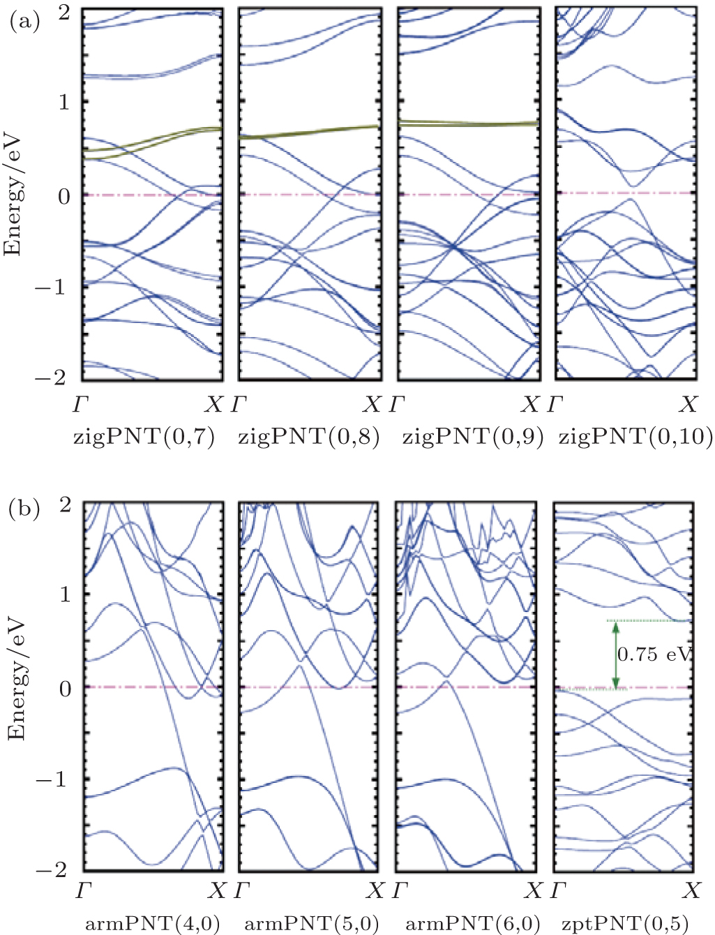 | Fig. 7. Band structures of (a) zigPNTs, (b) zptPNT(0, 5) and armPNTs. The dark green lines indicate that the characteristic energy bands consist of local d orbital levels in phosphorus atoms and the band gap in zptPNT(0, 5) is 0.75 eV marked by dark green. |
Figure 7(a) shows that the band structures of smaller zigPNTs are significantly different from those of zigPNT(0, 10) and show metallic features. There are two energy bands close to each other as marked by the dark green lines, rather flat for zigPNT(0, 8) and zigPNT(0, 9), growing out of the highly localized d orbital levels in phosphorus atoms, similar to those observed by Seifert and Herná ndez in BP allotrope tubes where the d-basis functions also play an important role in describing the conduction band states, [36] but more localized here. When the local d orbital levels are close to the Fermi level, one of the lone-pair electrons in the sp3 orbitals can be easily turns into one of the d orbitals so that the I, II, III, and IV building-blocks including five covalent bonds can appear as shown in Fig. 5. Metallic characteristic in band structure is necessary for the phase transition, because it makes the electrons below Fermi level easy to jump, [6, 31] but the formation of new structures requires different bonding orbitals. As shown by Fig. 7(b), no narrow band consisting of local d orbital levels can be observed in the armPNTs, so it is difficult to supply new chemical bonds for bending-induced phase transition in armPNTs.
It can be seen from Fig. 7(b) that the transition from zigPNT(0, 5) to zptPNT(0, 5) is more likely to be a Peierls transition as the lattice has been distorted seriously with a metal-to-semiconductor transition which opens a band gap of 0.75 eV, very similar to armchair carbon nanotubes which become semiconducting at low temperature.[37] However, the metallic characteristics of other zptPNTs still remain in band structures when the zigPNTs transfer into zptPNTs which cannot be easily explained by Peierls transition (see Appendix E). As a quasi-one-dimensional material, the zigPNTs remain the properties and structures of phosphorus monolayer so that phosphorus atoms are much more tightly linked together after wrapping the BP monolayer into nanotubes. In some cases a stabilizing deformation leads to the formation of a real band gap. In other cases, a deformation is effective in producing bonds, thereby pulling some states down from the Fermi level region. Because of the preserved two-dimensional linkage it may not be possible to remove all the states from the Fermi level region. Some density of states remains there and the material may still be a conductor. So the zigPNT(0, 7), zigPNT(0, 8), and zigPNT(0, 9) transfer into their new stabilizing structural phases, and the metal properties are still preserved.
In this study, the bending-induced phase transition of BP is found through comprehensive DFT calculations. When wrapping the BP monolayer into nanotubes along the zigzag directions, phase transition occurs when curvature radius is smaller than that of zigPNT(0, 10), or 5 Å . The zigzag nanotubes with the odd numbered BP unit cells transfer toward armchair-like phases, but there appear the tubes with even numbered BP unit cells consisting of new building-blocks. Analyses of the bending strain energies, electron density distributions, and band structures reveal the mechanism for the induced phase transition by bending along the zigzag direction. However, bending along the armchair direction cannot induce any phase transition even down to curvature radius of 3 Å at (4, 0) armchair BP nanotube. The results mean that it is possible to fabricate larger layered BP by mechanical cleavage along the armchair direction.
| 1 |
|
| 2 |
|
| 3 |
|
| 4 |
|
| 5 |
|
| 6 |
|
| 7 |
|
| 8 |
|
| 9 |
|
| 10 |
|
| 11 |
|
| 12 |
|
| 13 |
|
| 14 |
|
| 15 |
|
| 16 |
|
| 17 |
|
| 18 |
|
| 19 |
|
| 20 |
|
| 21 |
|
| 22 |
|
| 23 |
|
| 24 |
|
| 25 |
|
| 26 |
|
| 27 |
|
| 28 |
|
| 29 |
|
| 30 |
|
| 31 |
|
| 32 |
|
| 33 |
|
| 34 |
|
| 35 |
|
| 36 |
|
| 37 |
|
| 38 |
|
| 39 |
|