Zeng Jian, Liu Jie†, Zhang Sheng-Xia, Zhai Peng-Fei, Yao Hui-Jun, Duan Jing-Lai, Guo Hang, Hou Ming-Dong, Sun You-Mei. Irradiation effects of graphene and thin layer graphite induced by swift heavy ions. Chinese Physics B, 24(8): 086103
Permissions
Irradiation effects of graphene and thin layer graphite induced by swift heavy ions
Zeng Jiana), Liu Jie†a), Zhang Sheng-Xiaa),b), Zhai Peng-Feia), Yao Hui-Juna), Duan Jing-Laia), Guo Hanga),b), Hou Ming-Donga), Sun You-Meia)
Institute of Modern Physics, Chinese Academy of Sciences (CAS), Lanzhou 730000, China
University of Chinese Academy of Sciences, Beijing 100049, China
*Project supported by the National Natural Science Foundation of China (Grant Nos. 11179003, 10975164, 10805062, 11005134, and 11275237).
Abstract
Graphene and thin graphite films deposited on SiO2/Si are irradiated by swift heavy ions (209Bi, 9.5 MeV/u) with the fluences in a range of 1011 ions/cm2–1012 ions/cm2 at room temperature. Both pristine and irradiated samples are investigated by Raman spectroscopy. For pristine graphite films, the “blue shift” of 2 D bond and the “red shift” of G bond with the decrease of thickness are found in the Raman spectra. For both irradiated graphene and thin graphite films, the disorder-induced D peak and D′ peak are detected at the fluence above a threshold Φth. The thinner the film, the lower the Φth is. In this work, the graphite films thicker than 60 nm reveal defect free via the absence of a D bond signal under the swift heavy ion irradiation till the fluence of 2.6 × 10¹² ions/cm2. For graphite films thinner than 6 nm, the area ratios between D peak and G peak increase sharply with reducing film thickness. It concludes that it is much easier to induce defects in thinner films than in thicker ones by swift heavy ions. The intensities of the D peak and D′ peak increase with increasing ion fluence, which predicts the continuous impacting of swift heavy ions can lead to the increasing of defects in samples. Different defect types are detected in graphite films of different thickness values. The main defect types are discussed via the various intensity ratios between the D peak and D′ peak ( HD/ H D′).
PACS:
61.82.–d; 61.72.Hh
Keyword:
graphene; thin graphite films; swift heavy ions; irradiation effect
Graphene is a purely single atomic layer of hexagonal sp2 bonded graphite, which could be viewed as a building block comprised of various carbon allotropes, e.g. buckyballs, nanotubes, and others carbon materials. It has become a hot topic since the existence and stability of monolayer graphene were discovered.[1] The potential application prospect and the remarkable electronic properties of this material have aroused the increasing interest. It exhibits high crystal quality, ballistic transport on a submicron scale and its electron transport could be described by the Dirac equation. The outstanding properties render it a new material option for electronic application.[2– 5] However, the perfect transport properties depend largely on the defect-free layer structure. The defects and impurities in monolayer and few-layer graphene have strong influences on their electronic properties[6] and the realistic potential of applications. Moreover, controlled introduction of defects into the perfect lattice is required in the proposed future applications of graphene.[7] The investigation of defects in graphene is of crucial importance for understanding and predicting the property of the various carbon allotropes and graphene devices.
Recently, different aspects of ion irradiation-induced damage to graphene have been investigated experimentally. The effects of plasma treatment, electon beam irradiation, [8– 10] and low energy ion beam irradiation[11– 15] in a controlled way on graphene sheets have been studied to ascertain the evolution of crystalline order and electronic properties with the introduced defects. However, experimental reports on these defects are limited, and most of the investigations deal with the low and medium energy electron– beam irradiation or the projectiles in the eV to keV energy regime. In this energy regime the stopping process of the ions is dominated by elastic collisions, and the damage is due to nuclear collisions between impacting ions and carbon atoms. Only a few studies have been performed with swift heavy ions of several MeV per nucleon.[16] The swift heavy ions deposit their energy mainly by electronic excitations via inelastic collisions with target electrons, thereby causing excitation and ionization processes.
In order to investigate the influence of the sample thickness on irradiation effects, graphene and thin graphite films are irradiated by 209Bi ions with different energies and fluences at room temperature. Different Raman features of pristine samples with various thickness values are detected. Moreover, the irradiation effects of graphene and thin graphite films are investigated by Raman spectroscopy. The evolution of the Raman spectrum with increasing sample thickness shows that under the same irradiation condition, different thickness graphite films have different types of defects, and more serious damages can be induced in thinner graphite films.
2. Experiment
The Si wafers with a 300-nm SiO2 capping layer were used as the substrate for the graphene, according to the principle of optical reflection and refraction, the thin graphite films on SiO2/Si substrate can be visualized by optical microscopy.[17] Letter and number marks were made on the top surface of SiO2/Si by electron beam lithography. The space between two marks was about 250 μ m. These marks could be used to determine the candidate of graphene sheets for the repeatable test operation. The SiO2/Si wafers with marks were diced into 7 μ m× 7 μ m× 1 μ m, and cleaned as the standard procedure.
The monolayer graphene and thin graphite films were produced in air at room temperature by micromechanical cleavage of highly ordered pyrolytic graphite (HOPG, Advanced Ceramics Co., Grade ZYB). The peel flakes from HOPG were transferred to SiO2/Si substrate by adhesive tape. An optical microscope was used to identify the graphene sheets. The letter and number marks nearby the graphene sheets were recorded for the following experiment and tests.
The 209Bi ions with an initial kinetic energy of 9.5 MeV/u was provided by two cyclotrons of Heavy Ion Research Facility in Lanzhou (HIRFL) of Institute of Modern Physics (IMP). The graphene and thin graphite films were irradiated by 209Bi ions with fluences in a range of 1011 ions/cm2– 1012 ions/cm2 at room temperature. In order to reduce ion energy and adjust the electronic energy loss, the aluminum foils of different thickness values were used as degraders in front of graphene and thin graphite films. The purity of each of the aluminum foils is 99.99%.
The microscopic confocal Raman spectrometer (LabRAM HR800, Jobin Yvon Co.) was used to characterize both the pristine and irradiated graphene and thin graphite films. The excitation wavelength of Raman spectrometer was 532 nm. A long working distance objective lens of 50 times was chosen to avoid the possible damage introduced by the laser of Raman spectrometer in the testing process. The monolayer and bilayer graphene were identified by the Raman spectra via the inspection of the full width at half maximum (FWHM) of 2D peak around 2700 cm− 1.[18]
The atomic force microscope (MFP– 3D– SA, AFM), which is a direct method to identify single and few layers graphene, was used to confirm the thickness values of the graphene sheets and thin graphite films.
Scanning tunneling microscope (STM) measurement offers an accurate measure of the defect morphology and density. The surface of irradiated HOPG was observed by STM with mechanical sheared Pt– Ir tips at room temperature. The scanning area was minimized from 200 nm2 to 8 nm2 in which the atomic scale was reached.
3. Results and discussion
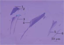
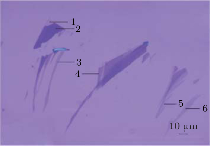
The monolayer graphene and graphite films produced by micromechanical cleavage are deposited on SiO2/Si as shown in Fig. 1. The morphologies of thin graphite films are easily mapped by optical microscope according to the refraction principle of light. Number marks present the different parts of graphite films with various thickness values identified by the different colors.
Fig. 1. Optical microscopy image on sample containing graphene sheets of different thickness values exfoliated onto an SiO2/Si substrate. Graphite films with different thickness values are marked by numbers.
The microscopic Raman spectrometer is used to characterize the different thin graphite films marked by numbers. The measurements are performed in backscattering geometry at room temperature. The position and the integrated intensity of the peaks are analyzed by Lorentz peak fitting.
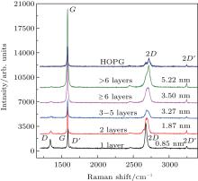
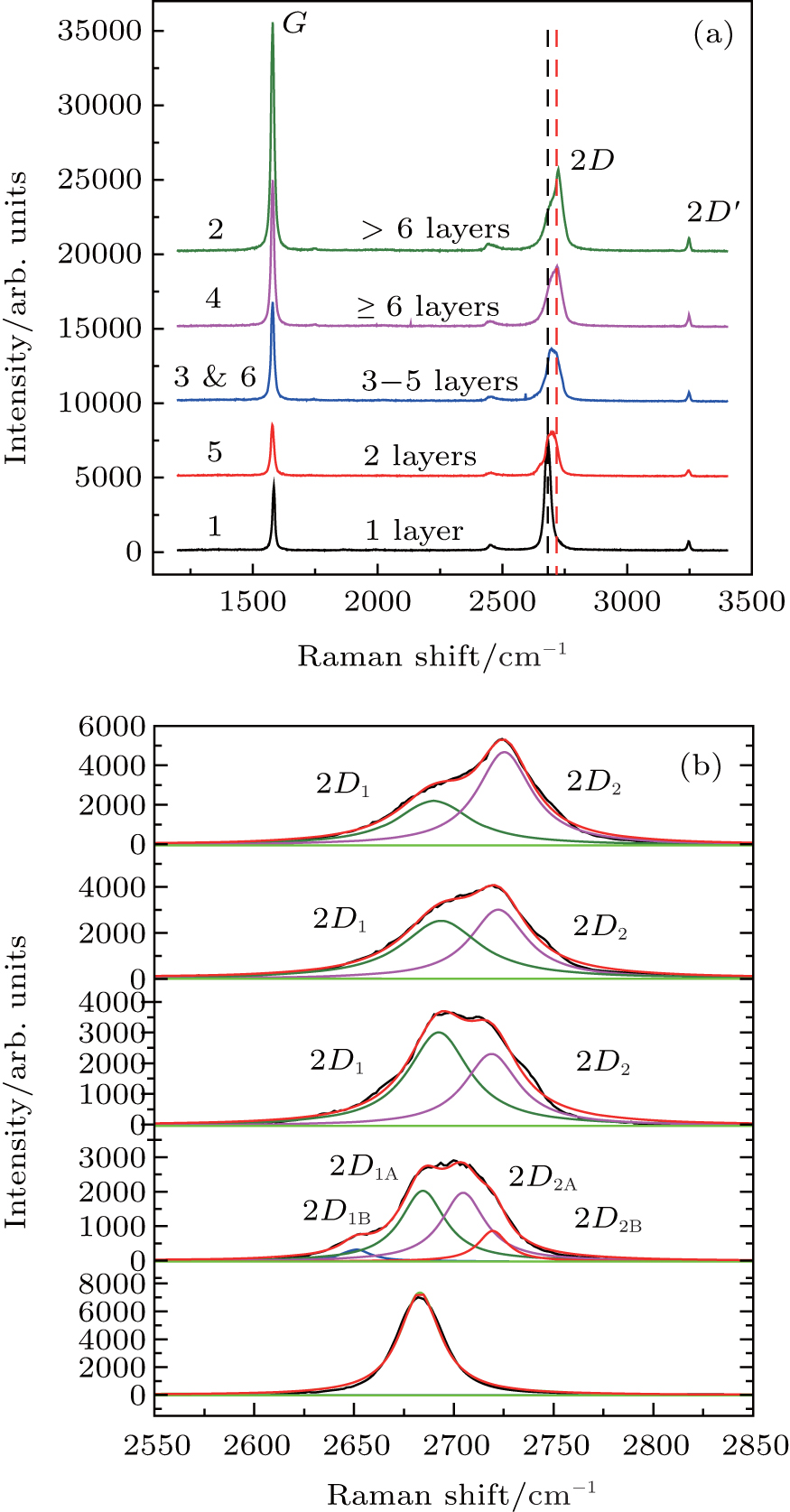
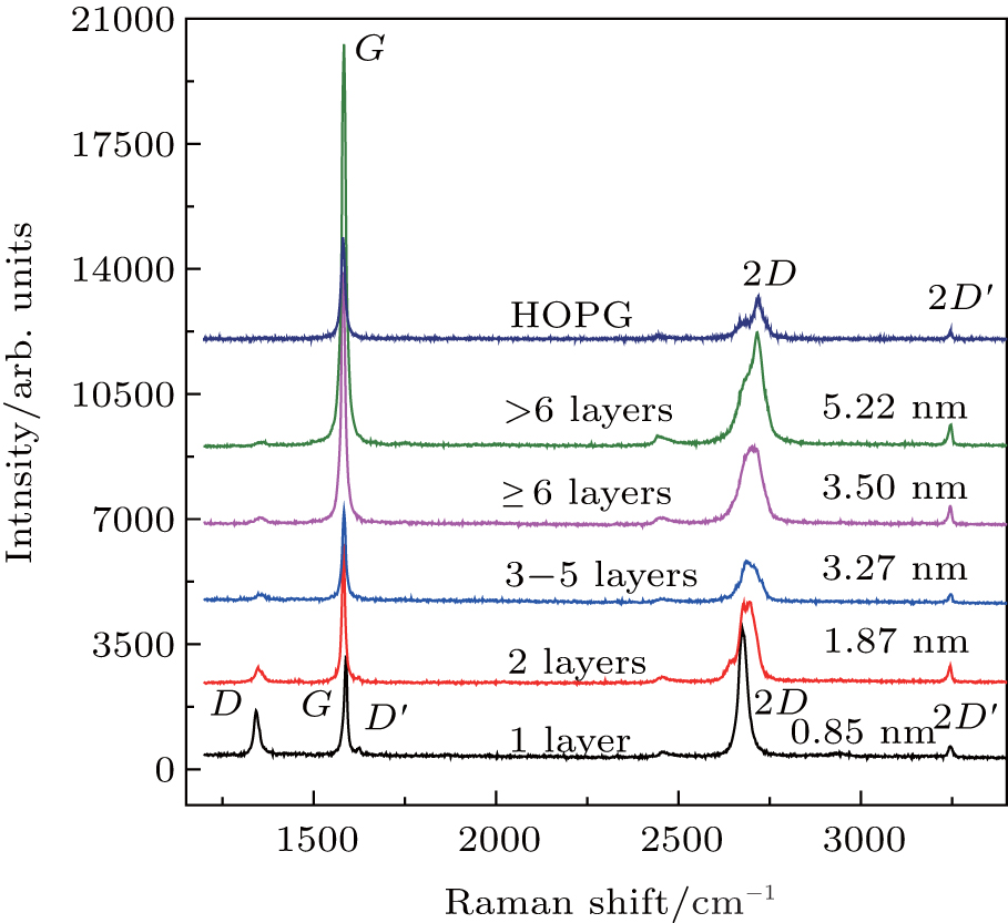
The Raman spectra obtained from different regions of pristine samples are shown in Fig. 2. The virgin sample has three important features: G peak (∼ 1582 cm− 1), 2D peak (∼ 2683 cm− 1), and 2D′ peak (∼ 3242 cm− 1). Compared with the peaks in Raman spectrum of HOPG, [19] the G peak in the first-order spectrum can be attributed to the Raman active E2g phonon close to the Γ point. The 2D historically named G′ peak is unrelated to G peak, but is the second order of zone-boundary phonons. They are not seen in first order Raman spectra since zone-boundary phonons do not satisfy the Raman fundamental selection rule. As reported in Refs. [18]– [23], the second order 2D Raman peaks are sensitive to the number of thin graphite films. The single-layer, bilayer, and few-layer graphenes have their own unique Raman fingerprints. As shown in Fig. 2(b), the monolayer graphene has a very sharp 2D bond (∼ 2681 cm− 1), which could be fitted by a single Lorentzian peak. For bilayer graphene, the 2D peak is much broader. Four components: 2D1B (∼ 2651 cm− 1), 2D1A (∼ 2685 cm− 1), 2D2A (∼ 2705 cm− 1), and 2D2B (∼ 2719 cm− 1) could be obtained by Lorentz peak fitting. These four components could be attributed to electronic bands effects of bilayer graphene.[18] For three-layer graphene, the Raman spectrum could be divided into two Lorenz peaks 2D1(∼ 2692 cm− 1) and 2D2(∼ 2719 cm− 1), and the intensity of 2D1 peak is obviously larger that of 2D2 peak. The further increase in layer number leads to a significant intensity decrease in 2D1 peak and increase in 2D2 peak. The intensity of 2D2 peak would be larger than 2D1 peak when the film is thicker than 6-layer graphene. Actually, the 2D Raman spectrum for more than 6 layers is hard to distinguish from that of bulk graphite. Graphene sheet more than 50 layers could be view as bulk graphite. The dashed lines in Fig. 2(a) show the shift of 2D peak center with the increase of the number of graphene layers. The up shift is primarily caused by the increase of 2D2 component.
Fig. 2. Raman spectra of pristine thin graphite films exfoliated onto an SiO2/Si substrate: (a) different Raman spectra of the graphite films with different thickness values, (b) the Lorentz peak fitting of the 2D peak corresponding to single- and few-layer graphene flakes in panel (a). The numbers on the left side of the spectra in panel (a) are corresponding to number marks of the graphene flakes in Fig. 1.
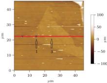
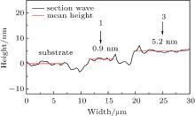
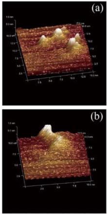
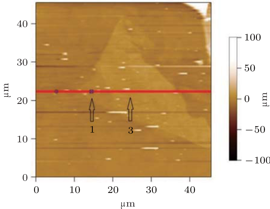
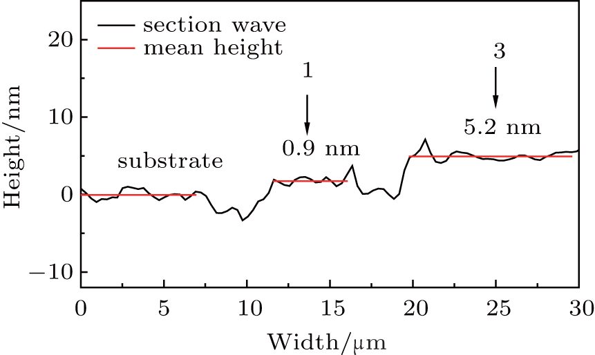
The Raman spectra could be used to distinguish the single layer, bilayer graphenes from multiple layers (≥ 3 layers) and bulk graphite by the Raman fingerprints of 2D bond. However, 2D peaks of 3– 6 layers have no recognizable difference among them, and the intensity ratio between 2D1 and 2D2 can only give qualitative analysis of the thickness. For more than 6 layers, the number of layers is unable to be confirmed by Raman spectra. Non-contact mode AFM test offers the quantitative analysis of thickness of the thin graphite film. Figure 3 shows the AFM image of graphene and different thickness values of graphite films. The relative section wave is shown in Fig. 4. The thin horizontal line is the average height of the fragments. The thickness values of the thin graphite films could be confirmed by the height difference along this line. For example, the thickness values of HOPG sheets marked “ 1” and “ 3” are 0.9 nm and 5.2 nm, respectively.
Fig. 3. AFM image acquired on a 45 μ m× 45 μ m scan area on graphene and different thickness graphite films deposited on SiO2/Si. The number marks 1 and 3 are corresponding to the marks with the same number of optical microscopy image of HOPG fragments.
Fig. 4. Section wave related to the line crossing the AFM image of the graphite film. The thin horizontal line is the average value of the film height. The thickness values of graphene and thin graphite films could be indicated by calculating the height difference.
According to the Raman spectrum of graphite fragment marked by number 1, shown in Fig. 2(a), the 2D Raman bond is symmetrical, and the height ratio between 2D peak and G peak is about 2.38. Then the piece of graphite film marked with “ 1” could be confirmed as defect free monolayer graphene. The thickness of graphene obtained from AFM is about 0.9 nm as shown in Fig. 4, which is in agreement with the result of 0.9 nm reported by Novoselov et al.[24] However, the thickness of 0.9 nm is much larger than the theoretical thickness of 0.34 nm for monolayer graphene. This may be due to the low throughput of AFM. Moreover, the chemical contrast between graphene and the substrate will lead to an apparent chemical thickness of 0.5 nm– 1 nm.[1, 24]
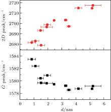
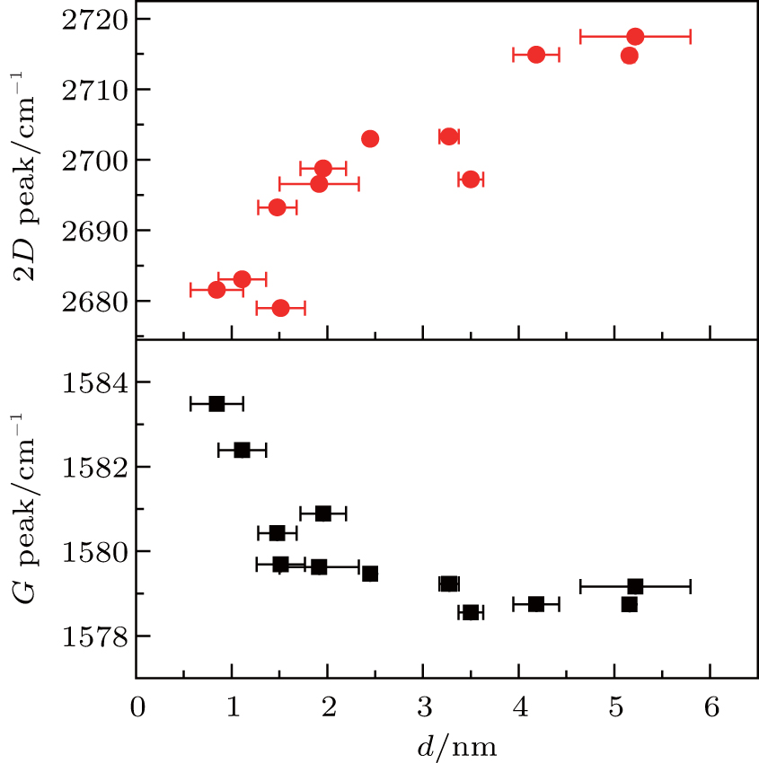
Different flakes of graphite films are investigated by both Raman spectroscopy and AFM. Different peak centers of G peak and 2D peak are detected in samples with various thickness values. The evolution of the peak center with the increasing thickness is shown in Fig. 5. The frequency of G peak shifts towards higher wave number at the crossover for thinner layers and especially for the double- and single-layer graphenes. On the contrary, the frequency of 2D peak swifts to lower wave number as the decrease of the film thickness.
Fig. 5. The G peak and 2D peak positions of pristine single layer and thin graphite films of different values of thickness d.
As shown in Fig. 2, the Raman spectra reveal defect-free graphite sheets via the absence of a D bond signal. After irradiation by 578 MeV 209Bi ions with a fluence of 1.3 × 10¹¹ ions/cm2, the same samples are characterized by Raman spectrometer. The Raman spectra of irradiated sample are shown in Fig. 6. The thickness values of different graphite sheets are detected by AFM and marked beside the Raman data. For irradiated graphite sheets, new peaks defined as D peak (∼ 1339 cm− 1) and D′ peak (∼ 1621 cm− 1) appear. The D peak is physically related to the in-plane breathing mode of the carbon hexagonal ring (A1g symmetry). According to Reich and Thomsen’ s study, [25]D peak and D′ peak are the two most prominent features in the disorder-induced graphite Raman spectrum. For bulk graphite, the obvious D peak appears only when the fluence exceeds a threshold value Φ th[26] and the relative Raman intensities of these two peaks are on the order of ID/ID′ ≈ 10. Then the obvious D′ peak could be obtained only when the fluence is high enough. No D peak could be found in Raman spectrum of irradiated HOPG nor in that of HOPG films thicker than 60 nm under the same irradiation condition. Calculated by the stopping and range of ions in Matter-2013 (SRIM-2013), the electronic energy losses of Bi with energies of 1.2 GeV, 973 MeV, and 578 MeV are 25.7 keV/nm, 26.4 keV/nm, and 26.5 keV/nm, respectively. As reported by Liu et al.[27] the threshold of electronic energy loss for surface track creation is 7.3 ± 1.5 keV/nm. In this work, the images of HOPG surface irradiated by 578 MeV 209Bi are detected by STM.
Fig. 6. Raman spectra of different thickness graphite films irradiated by 209Bi with energy 578 MeV and fluence 1.3 × 10¹¹ ions/cm2.
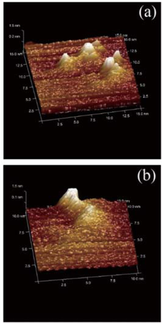
As shown in Fig. 7, hillocks are detected on the graphite surface after irradiation, which is in good agreement with the previous result obtained by Liu et al.[27] Then the absence of a D bond signal in graphite film thicker than 60 nm, which could be viewed as bulk HOPG, reveals that the defects are not serious enough to be detected by Raman spectrometer. In fact, for bulk HOPG, the D peak appears only when the fluence exceeds a threshold value Φ th[26] and due to the special single atomic layer structure of graphene, the irradiation fluence threshold Φ th of the D band of graphene is significantly lower than that of HOPG.[28] The situation is much more complicated in thin layer HOPG films, and the Φ th must be related to the sample thickness. As shown in Fig. 6, for monolayer graphene, both of the D peak and D′ peak come out after irradiation. While for bilayer graphene, only the D peak shows up. The intensity of the D peak decreases with increasing thickness. This indicates that the Φ th values of graphite films are different. The thinner the film, the smaller the Φ th is. It is proved that the thinner graphite films are much easier to destroy by swift heavy ion irradiation than thicker ones. More work needs to be done to ascertain the relationship of the Φ th with the sample thickness.
Fig. 7. STM images of HOPG irradiated by 578-MeV Bi with a fluence of 2.6× 10¹² ions/cm2. The scan areas are (a) 15 nm× 15 nm and (b) 10.2 nm× 10.2 nm.
In order to investigate the evolutions of the disorder peaks, more graphene and thin graphite films are irradiated by 209Bi ions with different energies and fluences. The evolutions of Raman spectra with the different film thickness values are shown in Figs. 8(a)– 8(c). These thin films are irradiated by 1.2-GeV 209Bi ions with fluences of 1.3 × 10¹¹ ions/cm2, 6.5 × 10¹¹ ions/cm2, and 2.6 × 10¹² ions/cm2. The D peak and D′ peak come out after irradiation, which predict that the defects form in both irradiated monolayer graphene and thin graphite films. For the same irradiation fluence, the intensities of the D peak and D′ peak obtained from films with various thickness values are different. The monolayer graphene has the most obvious D peak and D′ peak. The intensities of the D peak and D′ peak decrease with increasing thickness, and finally disappear when the film is thick enough. As mentioned earlier, this indicates that the single layer graphene has the weaker anti-irradiation property than the thicker graphite films. Comparing the Raman spectra of graphite films irradiated by different ion fluences shown in Figs. 8(a)– 8(c), we could figure out that for graphite films with the same thickness, the intensities of the D peak and D′ peak increase with increasing fluence. This predicts that the continuous impacting of swift heavy ions would lead to increasing defects in samples.
Fig. 8. Raman spectra of thin graphite films of different thickness values irradiated by 1.2-GeV 209Bi with fluences of (a) 1.3 × 10¹¹ ions/cm2; (b) 6.5 × 10¹¹ ions/cm2; (c) 2.6 × 10¹² ions/cm2.
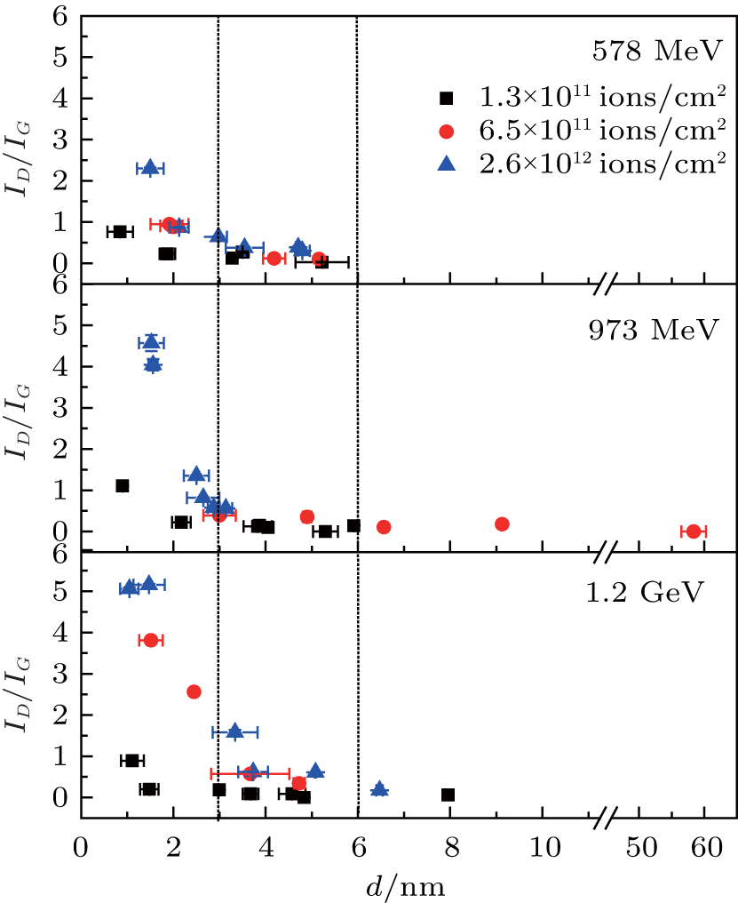
The area ratios between D peak and G peak, ID/IG, from different thickness graphite films irradiated by 209Bi with different energies and fluences are shown in Fig. 9. The ID/IG increases slowly as film thickness decreasing during the 6 nm– 3 nm period, which indicates that the D line appears and the intensity grows with the decrease of thickness. The ID/IG rises sharply when the film thickness decreases from 3 nm to about 1 nm. For all of the irradiation fluences, the single layer graphene has a maximal ratio of ID/IG. The most serious defects could be concluded in single layer graphene after irradiation. More work needs to be done to check whether a threshold value Φ exists. When the thickness is lower than Φ , the properties of the thin graphite films are totally different from those of bulk graphite.
Fig. 9. Evolutions of ID/IG of Raman spectra from different thickness graphite film samples irradiated by 209Bi ions with different energies.
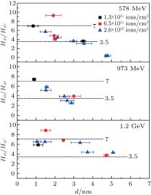
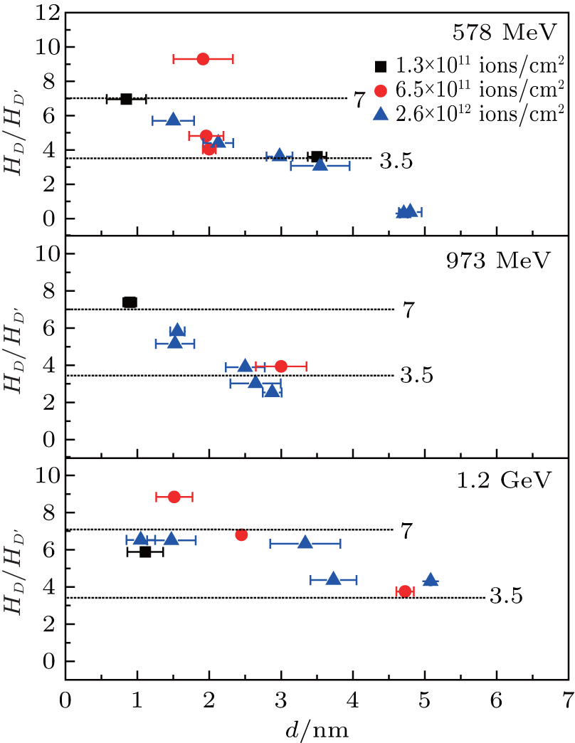
According to Eckmann et al.’ s results[29] the relative intensities of D peak and D′ peak (HD/HD′ ) depend on the type of the defects. The HD/HD′ is maximum (∼ 13) for defects associated with sp3 hybrization, and it decreases for vacancy-like defects (∼ 7) and reaches a minimum for boundaries in graphite (∼ 3.5). Figure 10 shows the HD/HD′ values versus thickness for all of the graphite films tested. As mentioned previously, the D′ peak shows up only when the fluence is high enough. Even at the highest fluence of 2.6 × 10¹² ions/cm2 of our experiment, D′ peak could be detected only when the graphite film is thinner than 6 nm. For the graphite films irradiated by 579-MeV Bi ions with a fluence of 2.6 × 10¹² ions/cm2, the minimum HD/HD′ is about 3.5, which is corresponding to the boundaries in graphite as Axel Eckmann et al.[29] reported. Then the HD/HD′ increases with film thickness decreasing and reaches the highest value of 6, which means that the main type of defect is vacancy-like defects. The increase of HD/HD′ with thickness decreasing is also found in graphite films irradiated by 973-MeV and 1.2-GeV Bi ions with different fluences, as shown in Fig. 10, indicating that under the same irradiation condition, the main defect types of various thickness graphite films are different.
Fig. 10. Evolutions of HD/HD′ obtained from different thickness graphite films irradiated by different energy 209Bi ions.
4. Conclusions
The pristine single layer graphene and thin graphite films exfoliated onto an SiO2/Si substrate are investigated by Raman spectroscopy and AFM to confirm the existence of single layer graphene and the thickness values of different graphite films. The monolayer and bilayer graphenes could be easily distinguished via the Raman fingerprint while other layers should be identified by AFM. For different thickness graphite films, the “ blue shift” of 2D bond and the “ red shift” of G bond with the decrease of thickness were found in the Raman spectra. After the irradiation of 209Bi ions with energies ranging from MeV to GeV, the disorder-induced peaks of D band and D′ band are detected after irradiation till the threshold fluence Φ th, indicating the damage happens to the lattice. No D peak is detected at the graphite films thicker than 60 nm till the fluence of 2.6 × 10¹² ions/cm2. It is found that the thinner the film, the smaller the Φ th is. For both monolayer graphene and thin graphite films, the intensities of the D peak and D′ peak increase with increasing fluence. At the same ion fluence, the ratio of ID/IG decreases sharply with the film thickness and drops down to zero when the sample is thick enough, which indicates that the thinner the film, the more the defects induced in the film irradiated by the same number of heavy ions. The monolayer graphene has the weakest anti-irradiation properties relating to thick graphite. Moreover, under the same irradiation condition, different defect types in the different thickness graphite films are discussed via the various HD/HD′ .
Acknowledgment
The irradiation experiment was performed at HIRFL of IMP. We would like to thank all the members of the accelerator team of HIRFL.
LuccheseM M, StavaleF, FerreiraE H M, VilaniC, MoutinhoM V O, CapazR B, AcheteC A and JorioA2010Carbon481592DOI:10.1016/j.carbon.2009.12.057[Cited within:1]
14
TapasztóL, DobrikG, Nemes-InczeP, VertesyG, LambinP and BiróL2008Phys. Rev. B78233407DOI:10.1103/PhysRevB.78.233407[Cited within:1]
EckmannA, FeltenA, MishchenkoA, BritnellL, KrupkeR, NovoselovK S and CasiraghiC2012Nano. Lett. 123925DOI:10.1021/nl300901a[Cited within:2]
2
2004
0.0
0.0
... [1] The potential application prospect and the remarkable electronic properties of this material have aroused the increasing interest ...
... [1,24] ...
1
2007
0.0
0.0
... [2#cod#x2013 ...
1
2007
0.0
0.0
1
2008
0.0
0.0
1
2006
0.0
0.0
... 5] However, the perfect transport properties depend largely on the defect-free layer structure ...
1
2006
0.0
0.0
... The defects and impurities in monolayer and few-layer graphene have strong influences on their electronic properties[6] and the realistic potential of applications ...
1
2009
0.0
0.0
... [7] The investigation of defects in graphene is of crucial importance for understanding and predicting the property of the various carbon allotropes and graphene devices ...
1
2004
0.0
0.0
... The effects of plasma treatment, electon beam irradiation,[8#cod#x2013 ...
1
2008
0.0
0.0
1
2009
0.0
0.0
... 10] and low energy ion beam irradiation[11#cod#x2013 ...
1
2009
0.0
0.0
... 10] and low energy ion beam irradiation[11#cod#x2013 ...
1
2009
0.0
0.0
1
2010
0.0
0.0
1
2008
0.0
0.0
1
2009
0.0
0.0
... 15] in a controlled way on graphene sheets have been studied to ascertain the evolution of crystalline order and electronic properties with the introduced defects ...
1
2011
0.0
0.0
... [16] The swift heavy ions deposit their energy mainly by electronic excitations via inelastic collisions with target electrons, thereby causing excitation and ionization processes ...
1
2007
0.0
0.0
... [17] Letter and number marks were made on the top surface of SiO2/Si by electron beam lithography ...
3
2006
0.0
0.0
... [18] ...
... [18]#cod#x2013 ...
... [18] For three-layer graphene, the Raman spectrum could be divided into two Lorenz peaks 2D1(#cod#x223C ...
1
1979
0.0
0.0
... Compared with the peaks in Raman spectrum of HOPG,[19] the G peak in the first-order spectrum can be attributed to the Raman active E2g phonon close to the #cod#x0393 ...
1
2007
0.0
0.0
1
2007
0.0
0.0
1
2007
0.0
0.0
1
2007
0.0
0.0
... [23], the second order 2D Raman peaks are sensitive to the number of thin graphite films ...
2
2005
0.0
0.0
... [24] However, the thickness of 0 ...
... [1,24] ...
1
2004
0.0
0.0
... s study,[25]D peak and D#cod#x2032 ...
2
2011
0.0
0.0
... th[26] and the relative Raman intensities of these two peaks are on the order of ID/ID#cod#x2032 ...
... th[26] and due to the special single atomic layer structure of graphene, the irradiation fluence threshold #cod#x03A6 ...
2
2001
0.0
0.0
... [27] the threshold of electronic energy loss for surface track creation is 7 ...
... [27] Then the absence of a D bond signal in graphite film thicker than 60 nm, which could be viewed as bulk HOPG, reveals that the defects are not serious enough to be detected by Raman spectrometer ...
1
2014
0.0
0.0
... [28] The situation is much more complicated in thin layer HOPG films, and the #cod#x03A6 ...
2
2012
0.0
0.0
... s results[29] the relative intensities of D peak and D#cod#x2032 ...
... [29] reported ...
Irradiation effects of graphene and thin layer graphite induced by swift heavy ions
[Zeng Jiana), Liu Jie†a), Zhang Sheng-Xiaa),b), Zhai Peng-Feia), Yao Hui-Juna), Duan Jing-Laia), Guo Hanga),b), Hou Ming-Donga), Sun You-Meia)]


 , Zhang Sheng-Xia