


Design and fabrication of structural color by local surface plasmonic meta-molecules
[Ma Ya-Qia) , Shao Jin-Haia) , Zhang Ya-Fengb) , Lu Bing-Ruia) , Zhang Si-Chaoa) , Sun Yanc) , Qu Xin-Pingd) , Chen Yi-Fang†a)  ]
]
]
|
|


†Corresponding author. E-mail: yifangchen@fudan.edu.cn
*Project partially supported by the National Natural Science Foundation of China (Grant No. 61205148).
In this paper, we propose a new form of nanostructures with Al film deposited on a patterned dielectric material for generating structural color, which is induced by local surface plasmonic resonant (LSPR) absorption in sub-wavelength-indented hole/ring arrays. Unlike other reported results obtained by using focus ion beam (FIB) to create metallic nanostructures, the nano-sized hole/ring arrays in Al film in this work are replicated by high resolution electron beam lithography (EBL) combined with self-aligned metallization. Clear structural color is observed and systematically studied by numerical simulations as well as optical characterizations. The central color is strongly related to the geometric size, which provides us with good opportunities to dye the colorless Al surface by controlling the hole/ring dimensions (both diameter and radius), and to open up broad applications in display, jewelry decoration, green production of packing papers, security code, and counterfeits prevention.
Unlike colorant-based pigmentation, structural color originates from the interaction of visible light with a structured surface by scattering, diffraction, interference, and reflection.[1, 2] For example, well-ordered arrangement of a periodic micro/nano-structure, known as photonic crystal, can strongly influence the light propagation.[3, 4] The pioneering research of conventional structural color by using three-dimensional (3D) periodical photonic crystals or multiple layer dielectrics can be traced back to the 17th century by Hooke (1665)[5] and Newton (1730).[6] However, due to the difficulty in fabricating the artificial 3D structures, few applications have succeeded so far. To avoid 3D lithography, Cowan proposed a multiple-step structure with a “ surface relief” configuration to mimic the naturally occurring structural color.[7] Although the simplified multiple-step structures on dielectrics have been theoretically proved to possess a coloring capability, its manufacture is still a daunting challenge. On the other hand, it was discovered that structural color can also be produced by periodically structured metal due to local surface plasmonic resonant (LSPR) absorption, [8] which has potential applications in micro-color filters, display, etc. However, this technique becomes limited when spatial resolution is a problem for the display application. Furthermore, the fabrication technique involves multiple layer nano-processing at a significantly high cost. In 2010, a new kind of structural color by local surface plasmonic resonant absorption from sub-wavelength-indented ring arrays was conceptually demonstrated.[9, 10] Although its “ intaglio” and “ bas-relief” structure explicitly proved the dramatic change and control of color by the geometry of metallic metamaterial in a continuous metal base, there are still a number of issues to be solved both theoretically and technically. First, the indented ring arrays on an expensive gold surface are constructed by focused ion beam (FIB) milling, which is not suitable for future applications in large-scale manufacturing; second, the intaglio (indented) ring trench in a gold surface has a width around 30 nm and depth from 30 nm to 80 nm, which is a big challenge for the current nanolithography technique; finally, the use of Au is not economic. All these problems become barriers for the practical applications of local surface plasmonic structural color (LSPSC).
In this paper, we propose a new type of sub-wavelength structure in continuous Al film on a patterned resist, that is, periodical hole/ring arrays, as shown in Fig. 1, aiming to gain an insight into LSPR color when Al is also utilized to develop a novel top– down nanofabrication approach. The importance of employing such a hole/ring array as periodical meta-molecules is that it has a surface relief configuration, suitable for top– down nanofabrications by either electron beam lithography (EBL) or prospectively nanoimprint lithography.
 | Fig. 1. Sub-wavelength (a) holes and (b) ring arrays in 200-nm thick Al film. The period of both two patterns is 400 nm. |
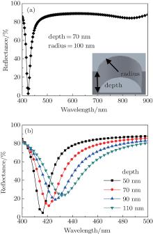
To study the optical behavior of the sub-wavelength hole/ring arrays in Al as illustrated in Fig. 1, a series of numerical simulations using finite-difference time-domains (FDTD) solutions (supplied by Lumerical Solutions, Inc.) is carried out. Figure 2 shows the simulated reflectance spectra by the hole arrays (meta-molecules) with a certain set of geometric sizes (as shown in Fig. 1(a)). For periodical hole arrays in Al film with a diameter of 100 nm for 400-nm lattice pitch and a depth of 70 nm, the reflectance spectra are presented in Fig. 2(a). The strong absorption peak around 400 nm in the spectrum should lead to the actual complementary color in Red/Green/Blue (RGB) palette. The absorption peak is strongly dependent on the hole geometry sizes, especially its radius and depth. As indicated in Fig. 2(b), by keeping the hole radius at 120 nm, and tuning the depth from 50 nm to 110 nm, the absorption peak shifts from around 415 nm to 435 nm. However, when changing the hole size, the absorption peak shifts only a little.
 | Fig. 2. Reflection spectra for structured aluminum surface with different holes arrays. (a) Single spectrum with the hole radius 100 nm and the depth 70 nm. A strong absorption can be observed around 420 nm in wavelength. (b) A series of reflection spectra for hole arrays in Al film with the same radius 120 nm, and the depths ranging from 50 nm to 110 nm. Clear absorption peak position shifts are observed, which means the color of structured Al is changing with the geometric size of the hole arrays. |
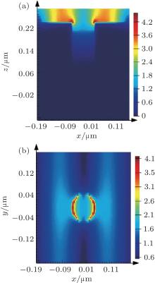
The incident light is coupled and trapped by such nano holes at a certain resonant wavelength which is determined by the geometry and dimensions (radius and depth in this case). This process is proved by the numerical simulations of spatial intensity of electric field with FDTD method as shown in Fig. 3. In the figure, the strong electric field in the corner of the hole indicates strong absorption and local field enhancement. For a small size of Al hole, the dipole is localized in a very small region with reduced dispersion in dipole dimension, resulting in a very sharp absorption in reflectance spectrum. The structural color seen from the structured metal is actually the complimentary color in the reflection spectrum after deduction of the absorption spectrum. This explains that the absorption peaks existing in the reflectance spectra originate from the local surface plasmonic resonance.
 | Fig. 3. FDTD simulation results for electric field distribution: (a) cross sectional view and (b) plan view for two adjacent holes at the response wavelength of absorption peak around 420 nm. The hole diameter is 50 nm for 400-nm lattice pitch with a depth of 70 nm. The color code is for the electric field intensity from low (dark blue) to high (deep red). |
It is also found in our work that absorption resonance in nanoscale holes is not so sensitive as that in rings. Therefore, a further study is carried out in periodical ring arrays. As shown in Fig. 4(a), the reflectance spectra are similar to those in hole arrays. However, with increasing the depth of the rings from 50 nm to 130 nm, with the width and radius unchanged, the position of the absorption peak shifts from 450 nm to 720 nm, covering most of the visible wavelength (Fig. 4(b)). When keeping both the width and depth of the rings fixed, the absorption peak shifts from 460 nm to 650 nm, and when increasing the outer radius from 100 nm to 180 nm it shifts toward the long wavelength end (Fig. 4(c)). Such a strong geometry effect on the LSPR property enables us to develop nanostructured Al film for color control in the full visible range. Figure 5 gives the relationships between absorption peak wavelength with the outer radius for different values of depth and width. It can be concluded that the proposed sub-wavelength ring arrays in Al are able to cover the structural color in a whole visible range.
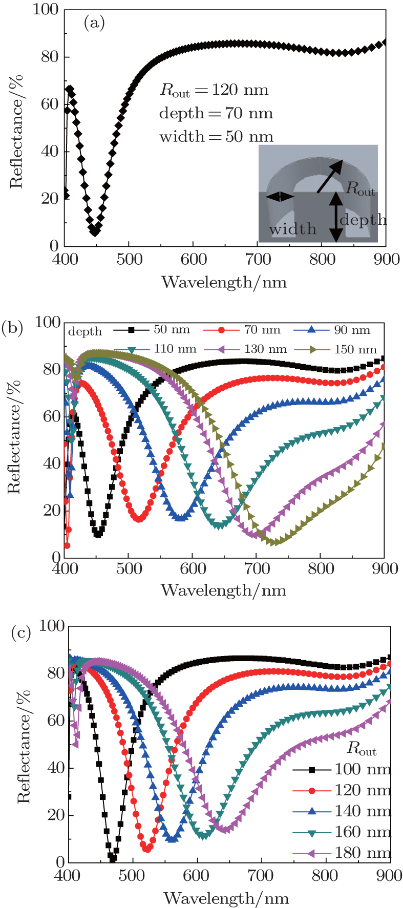 | Fig. 4. Reflection spectra for a structured aluminum surface with different rings arrays. (a) Single spectrum with the outer radius 120 nm, the width 50 nm, and the depth 70 nm. A strong absorption can be observed around 450 nm. (b) A series of reflection spectra for ring arrays in Al film with increasing depth while keeping the outer radius and width unchanged. The absorption peak shifts from 450 nm to 720 nm, covering the whole visible wavelength. (c) Reflection spectra for rings with the same depth and width, the absorption peak shifts from 470 nm to 650 nm with increasing outer radius. |
 | Fig. 5. Relationships between the position of absorption peak and the outer radius of the rings for different values of (a) depth and (b) width. |
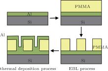
To verify the theoretical results as described above, optical measurements of ring/hole arrays are carried out. However, the fabrication of the proposed hole/ring arrays in this work is a big challenge because it contains nano-size holes/rings in Al film with the depth changing from 30 nm up to 150 nm. We develop a novel method using self-aligned metallization on pre-patterned polymethyl methacrylate (PMMA) to form the hole/ring array as illustrated schematically in Fig. 6. First of all, a 100-nm-thick Al is deposited on fresh clean Si wafer through physical vapor deposition (PVD). Then, the sample is spin-coated with a 300-nm-thick PMMA at 3500 rpm for 1 min after a layer of hexamethyl disilazane (HMDS) as adhesion layer, followed by a soft bake at 180 ° C in an oven for at least one hour. After that, e-beam exposure is carried out by using a state-of-the-art electron beam writer JEOL 6300FS with a beam current of 500 pA and a typical beam size of 8 nm at an accelerate voltage of 100 keV while the area dosage ranges from 50 μ C/cm2 to 800 μ C/cm2. Development process of the exposed resist proceeds in IPA/MIBK (3:1 in volume) for 1min at 23 ° C, followed by a rinse in IPA for 30 sec. Finally, a 100-nm thick Al film is deposited by thermal evaporation to form the desired hole/ring array structures. The 100-nm-thick Al layer deposited on Si wafer provides a continuous metal surface to mimic the rings/hole arrays in Al metal. The fabricated hole and ring arrays are inspected by using a Zeiss high-resolution scanning electron microscope (SEM) SIGMA HD as shown in Fig. 7. Figures 7(a) and 7(b) are SEM images for holes and rings before Al deposition, respectively. The hole diameter is 232 nm and the outer diameter of the ring is 287 nm for 400-nm lattice pitch, and the width is 50 nm with a depth of 300 nm, corresponding to the thickness of PMMA. After depositing a 100-nm-thick Al layer, the SEM images for both (c) hole arrays and (d) ring arrays are given.
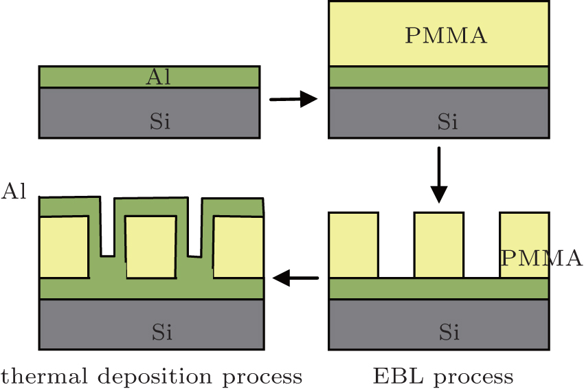 | Fig. 6. Process flow of Al metamaterial with sub-wavelength hole/ring arrays combined with e-beam lithography and thermal deposition process. |
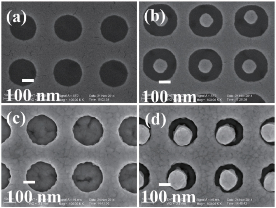 | Fig. 7. SEM images for (a) hole arrays in PMMA, (b) ring arrays in PMMA, (c) hole arrays in Al/PMMA, (d) ring arrays in Al/PMMA. The nano pillars fall when taking the SEM photos. |
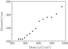
This method provides a rather simple way to form 2D hole/ring arrays in Al film by combining the EBL process with a metallization process, avoiding complicated nanofabrication processes such as reactive ion etch (RIE) or unreliable lift-off. The hole/ring size can be readily varied by tuning the exposure dosage. Figure 8 shows the resulting hole radius changing with the exposure dose. From the slope of the curve, 49-nm change in the hole diameter demands 646 μ C/cm2 dose latitude, indicating the developed process is stable with a pretty broad process window, thus allowing precise control of hole/ring size by tuning the exposure dose.
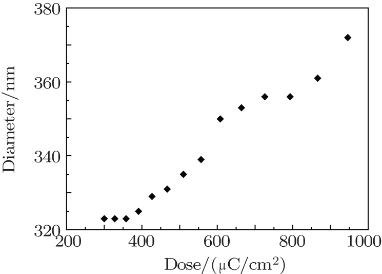 | Fig. 8. Variation of measured diameter of hole in PMMA with exposure dose in the EBL process. |
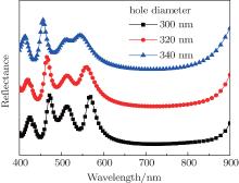
The optical property of the fabricated 2D Al hole/ring arrays is experimentally characterized by spectral approach. In order to measure the reflection spectra with normal incidence to the aluminum metamaterial, a micro-spectrum analyzer, which consists of a tungsten lamp light source, a microscope (Leica DM6000 M, Germany) and an optic spectrometer (range 400 nm– 8000 nm, SpectraPro 500i, Acton Research Co., USA) is employed. An optical microscope was utilized to observe the color as shown in Fig. 9(a). The color of the structured aluminum changes from purple to blue as the hole size increases from 240 nm to 334 nm for a 400-nm lattice pitch. Figure 9(b) clearly shows the blue shift of absorption resonance with increasing radius, which is consistent with the simulated results. The four curves are lifted from each other for clarity. By adjusting the geometry parameters of hole/ring arrays, the colorless aluminum is expected to generate the full range of colors for the whole color palette.
 | Fig. 9. (a) Optic microscope images of structured Al film with different holes; (b) measured reflection spectra for structured Al surface with different hole sizes. The curves are lifted apart for clarity. |
However, the actual spectra measured deviate from the simulated results (Figs. 2– 5). We understand that this is because the structures measured are different from those simulated as shown in Fig. 1. Based on the actual structures as shown in Fig. 6, a further simulation is carried out by using the same geometry parameters as those in the real samples. Figure 10 shows a new set of simulated reflectances. In a wavelength range from 400 nm to 600 nm, the simulated reflectance is qualitatively consistent with the measured behavior. With increasing radius, both the measured and simulated reflectance peaks move to the blue region. The big reflectance in the broad red area is attributed to the background in an unstructured Al surface, which also exists in the simulation results in Fig. 10. The broader peaks in Fig. 9 than those in Fig. 10 are probably caused by the fluctuations in radii in the real arrays. Nevertheless, both our numerical simulations and experimental results unambiguously demonstrate the structural color nature in the local surface plsamonic structure in a continuous Al film.
To achieve full range structural color stemming from LSPR in sub-wavelength metallic structure, we carry out systematic simulation by FDTD for resonant absorptions in hole arrays in Al film as a novel metamaterial. Al-based sub-wavelength meta-molecules, which are responsible for generating the novel structural color, are successfully fabricated by an EBL process combined with self-aligned Al deposition. Such a kind of structural color exhibits advantages in high resolution in color printing and low cost in fabrication. It possesses the great prospects in the applications of ultra-high resolution color display and imaging technology, high-density optical storage technology, miniaturized spectrophotometers, precious jewelry design, and anti-forgery technology.
The authors are grateful to the assistance by the staff in Nanolithography and Application Group at the Department of Microelectronics of Fudan University, Shanghai Institute of Technical Physics of the Chinese Academy of Sciences, and the Nanophotonic Group at the Department of Physics of Fudan University.
| 1 |
|
| 2 |
|
| 3 |
|
| 4 |
|
| 5 |
|
| 6 |
|
| 7 |
|
| 8 |
|
| 9 |
|
| 10 |
|