


A novel multi-pin rectangular waveguide slow-wave structure based backward wave amplifier at 340 GHz
[Zhang Kai-Chun†a), b)  , Qi Zhong-Kuo
a), b) , Yang Zhao-Longa), b) ]
, Qi Zhong-Kuo|
|


†Corresponding author. E-mail: zh.kch@163.com
*Project supported by the National Basic Research Program of China (Grant No. 2014CB339801) and the National High Technology Research and Development Program of China (Grant No. G060104012AA8122007B).
A backward wave amplifier (BWA) in a terahertz regime with a novel slow-wave structure (SWS) composed of multi parallel grating pins inside a rectangular waveguide is analyzed. The multi-pin rectangular waveguide SWS possesses good performance and is compatible with micro-fabrication technologies. The dispersion and interaction impedance of the multi-pin SWS are presented. The stopbands of the modes cling together in a Brillouim zone. The SWS has a high interaction impedance that is suitable for the interaction of multi cylindrical beams. The design, which is based on three parallel pins supporting the wave–beam interaction with four cylindrical beams, is verified by three-dimensional particle-in-cell simulations. A BWA with the central frequency at 340 GHz is demonstrated, and the output power is more than 100 mW. A tuning frequency range of 15 GHz (333–348 GHz) is obtained with a gain of more than 20 dB.
An amplifier in the terahertz frequency range has numerous applications in the fields of security, medicine, material science, and imaging. However, THz amplification[1– 9] is challenging due to its high losses and small dimensions. Hence, the developer of THz amplifiers has to confront these difficulties and reduce them as far as possible. In a backward wave amplifier (BWA), the beam line intersects the dispersion curve in the − 1 harmonic region and the group velocity is opposite to the electron beam flux. The BWA has the advantages of larger dimensions of the period that can be used for the same beam voltage compared to a traveling wave tube (TWT). Meanwhile, it is able to choose a higher interaction impedance and achieve a lower loss. Recently, a different approach was adopted in the EU FP7 optically driven terahertz amplifier (OPTHER) project for the design and realization of a 1 THz vacuum tube amplifier[1, 2] using a cylindrical electron beam with double corrugated rectangular waveguide slow-wave structure. An output power of 75 mW was predicted using an 11.6 kV, 4 mA (∼ 200 A/cm2) electron beam. In addition, a cascade BWA based on this conception was studied and it achieved a gain of about 15 dB using an 11.6 kV, 70 μ W, and 10 mA (∼ 800 A/cm2) electron beam with a high magnetic field (∼ 0.8 T) for electron beam compression and guiding.[3] However, the required current density and the magnetic field are too high and they result in a design difficulty. By using multiple beams, the required electron density should be greatly diminished, thereby simplifying the electron gun design and beam guiding.
An important air window lies at 340 GHz, and some application studies were carried out at this frequency, including radiation sources and wireless communication systems.[10– 15] In this paper, a BWA at 340 GHz with multi-cylindrical beams is proposed to be achieved by adopting a pin array slow-wave structure (SWS) in a rectangular waveguide. In Section 2, the cold parameter behavior is studied with three-dimensional (3D) electromagnetic simulations. In Section 3, an application of a three pin with four beams 340 GHz BWA is simulated with very low current density and magnetic field by PIC. In Section 4, two modern micro fabrication techniques are investigated for the multi-pin SWS.
The multi-pin rectangular waveguide SWS consists of a rectangular waveguide that includes multi-identical parallel pins. The pins are separated to form a channel through which an electron beam can pass. The use of multi-cylindrical beams can reduce the current density of single beam, and we can adopt the mature design and technical control of multi-beams. To show the characteristic of this type of SWS for a BWA, a structure with three parallel pins for four beams is studied.
The geometry of the SWS is shown in Fig. 1, with the geometric parameters denoted. Figure 1(a) shows a 3D view of the SWS, allowing multiple electron beams to propagate through the two-dimensional (2D) array pins. Figure 1(b) is a schematic diagram of the longitudinal section. Figure 1(c) is a schematic diagram of the transverse section. A longitudinal grating period d, air gap width s, grating height h, transverse pin period tw, and pin width ts are adopted in a rectangular waveguide of height b and width a. The parameter δ is the distance between the top of the pins and the center of the beam.
 | Fig. 1. Schematic diagrams of multi-pin rectangular waveguide SWS: (a) 3D model with multi beams, (b) longitudinal view, (c) multi-pin grating SWS transverse view. |
As a reference, we consider a structure designed for the 300– 400 GHz frequency range with a beam voltage of about 13 kV. The design can refer to the mode of the corrugated waveguide SWS.[16] The following dimensions are used: a = 1.05 mm, b = 0.48 mm, d = 0.14 mm, s = 0.08 mm, h = 0.15 mm, tw = 0.3 mm, ts = 0.15 mm. In the following section, all of the simulations are performed by CST Microwave Studio.[17]
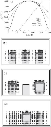
The dispersion curves are plotted in Fig. 2(a) as a function of kzd (the wave number normalized to the period d). There are three modes, TE10-like, TE20-like, and TE30-like modes, in the first Brillouim zone. The dispersion of a 13 kV electron beam is also shown in the figure. The electric field distributions of these three modes are shown in Figs. 2(b)– 2(d). For the multi-pin SWS, the mode number (in a Brillouim zone) is equal to the number of pins and the stopbands near the π point of these modes cling together. Furthermore, the cutoff frequency of the upper mode is higher than that of the lower mode.
 | Fig. 2. Dispersion and electric field distribution: (a) dispersions of 3 modes in the first Brillouim zone and the 13 kV electron beam; (b)– (d) electric field distributions of (b) TE10-like, (c) TE20-like, and (d) TE30-like modes on the transverse cross section. |
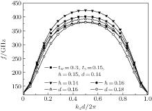
To analyze the influence on the dispersion, some different geometric parameters are used. Here, we only discuss the influence on the lowest order mode. The result is shown in Fig. 3, where the parameters remain unchanged unless given in the figure in units of mm. This figure shows that an increase of height h or period d lowers the dispersion curve.
 | Fig. 3. Dispersion relation versus different parameters. |
Here we discuss the impedance of SWS at the first backward wave space harmonic of the lowest order mode of the SWS where the BWA generally operates. In Fig. 4(a), the points A– F and O are on the boundary and the center of a cylindrical beam, respectively. The parameter δ is − 0.03 mm. The point G is at the position of x = a/2 and y = h+ 0.03 mm, which is the position of a sheet beam above the SWS, where a maximum impedance exists for a sheet beam as that of a corrugated waveguide SWS.[18] The impedances at different measured positions in the SWS are shown in Fig. 4(b). This indicates that the impedance on the circle beam cross section is inhomogeneous and the average is higher than that of the sheet beam. Therefore, with multi-cylindrical beams adopted, the beam– wave interaction in the SWS will be effectively enhanced.
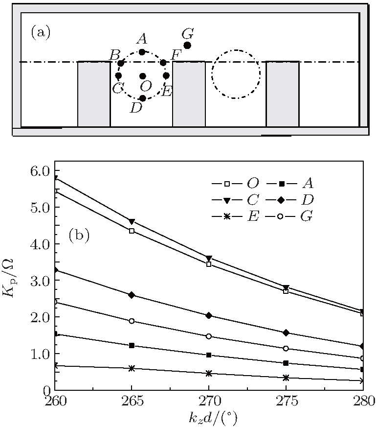 | Fig. 4. (a) Transversal section of the SWS with measured points, (b) impedance at different position as a function of kzd. |
With the geometry parameters given above, a backward wave amplifier at about 340 GHz is designed and simulated by CST Particle Studio.[17] A circuit consisting of 150 periods is shown in Fig. 5(a), which shows the input/output port and the beam tunnels with four homogeneous cylindrical beams. The input port is placed at the collector end, and the output port is placed at the electron gun end. The material of grating pins is copper with default conductivity σ = 5.88 × 10⁷ s/m in CST.
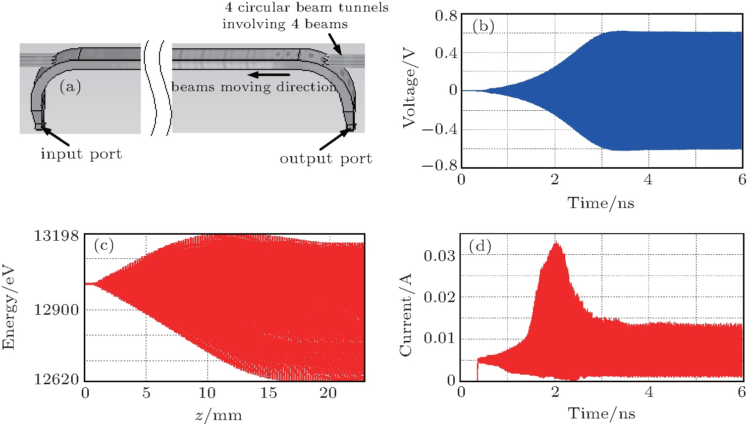 | Fig. 5. PIC simulation model and results: (a) 3D model with electric field distribution, (b) time domain spectrum on the output port, (c)electron energy modulation, (d) current bunching spectrum. |
The first step is to individuate the starting current of oscillation for a given beam voltage and number of periods of the SWS. The starting current is about 10 mA in the simulation with 13 kV beam voltage and 100 μ m beam diameter of the emitter.
The output power of the BWA is about 110 mW for this beam voltage, with total current 5 mA (∼ 4 A/cm2 per beam), focusing magnetic field 0.2 T, and input signal 338.03 GHz and 1.01 mW. Figure 5(a) shows the electric field distribution in the SWS, which indicates that the field is stronger near the output end and the operating mode is TE10-like. The voltage signal on the output port is shown in Fig. 5(b). By calculation, the output peak power is higher than 110 mW. Figures 5(c) and 5(d) show the electron energy modulation as a function of the SWS length and the current bunching varying with time, respectively.
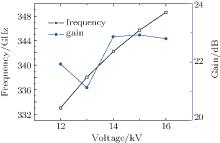
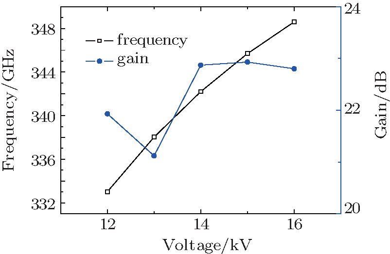
The amplified power and the gain are important parameters of a BWA. They vary with the beam voltage and the frequency of the input signal. To demonstrate the amplifying performance of the BWA, different cathode voltages 12– 16 kV with input signal of 330– 348.6 GHz and 1.01 mW are considered, while the beam current, period number, and focusing magnetic field are fixed at the original values. Figure 6 shows the relation of the gain with the voltage and the frequency. The gain is more than 20.5 dB with a tuning frequency range of 15 GHz. The gain is more than 40 dB with the PEC as the material of the prating pins in the frequency range of 330– 348.6 GHz.
 | Fig. 6. Relation of gain with beam voltage and input frequency. |
The fabrication of the SWS is a major challenge because the physical dimensions of the SWS are inherently small with a width of only 60 μ m and a depth of 150 μ m. We examine two techniques for manufacturing the circuit. One is electrical discharge machining (EDM) using 20 μ m diameter wire. A complication for the manufacturing is to keep the good surface finish, and to maintain the verticality and the uniformity of the pins. We fabricate a circuit with a total length of 150 periods and 3-row pins. A top view of the SWS circuit is shown in Fig. 7(a). There are small arcs on the bottom and the top of the pin because of the circle wire. Furthermore, the surface finish needs improving. The tolerance and the uniformity of the fabrication on the pin’ s section are less than 5 μ m, and the tolerance of the total length is about 20 μ m. However, due to the arcs, the tolerance of pin’ s depth is more than 10 μ m.
 | Fig. 7. Fabricated samples: (a) top view by EDM, (b) top view by LIGA. |
The other manufacturing technique is LIGA, which can be carried out in Beijing Synchrotron Radiation Facility (BSRF), Institute of High Energy Physics, Chinese Academy of Sciences. In the process, the PMMA resist is put on a Ti substrate with a thickness of 150 μ m and is then exposed to the synchrotron radiation x-ray through a mask. The PMMA structures are formed to supply the template for copper electroplating. Thus, the copper structures are produced on the Ti substrate. Sometimes, the copper height goes beyond this level when electroplating for a long time. The SWS is obtained by cutting the excess copper, wet etching the Ti substrate with HF acid, and removing the PMMA. Figure 7(b) shows the top view of the circuit obtained by LIGA. The circuit consists of 150 periods and 3-row pins. The uniformity of the pins is excellent with a tolerance of about 3 μ m. However, there are a few little bubbles on the base of the circuit, which need to be eliminated.
A multi-beam BWA for terahertz application is proposed by adopting an SWS consisting of multi-pins in a rectangular waveguide. Both the dispersion and the interaction impedance of the SWS have been studied. The SWS has many distinguishing characteristics. The cutoff frequency of the upper mode is higher than that of the lower mode, and their stopbands cling together in a Brillouim zone. The mode number in a Brillouim zone is equal to the number of pins. The impedance at different positions in the SWS is calculated by CST, which indicates that the structure assures an effective interaction for multi-cylindrical beams. By conducting a PIC simulation, we find that the BWA has a gain more than 20 dB and power above 100 mW in the range of 333– 348 GHz. This structure can be realized by modern micro fabrication techniques.
The authors appreciate the technical support of Researcher Yi Fu-Ting and Dr. Wang Bo during the design and fabrication with LIGA.
| 1 |
|
| 2 |
|
| 3 |
|
| 4 |
|
| 5 |
|
| 6 |
|
| 7 |
|
| 8 |
|
| 9 |
|
| 10 |
|
| 11 |
|
| 12 |
|
| 13 |
|
| 14 |
|
| 15 |
|
| 16 |
|
| 17 |
|
| 18 |
|