


Effect of body biasing on single-event induced charge collection in deep N-well technology
[Ding Yia) , Hu Jian-Guo†a)  , Qin Jun-Rui
b) , Tan Hong-Zhoua) ]
, Qin Jun-Rui|
|


†Corresponding author. E-mail: hujguo@mail.sysu.edu.cn
As the device size decreases, the soft error induced by space ions is becoming a great concern for the reliability of integrated circuits (ICs). At present, the body biasing technique is widely used in highly scaled technologies. In the paper, using the three-dimensional technology computer-aided design (TCAD) simulation, we analyze the effect of the body biasing on the single-event charge collection in deep N-well technology. Our simulation results show that the body biasing mainly affects the behavior of the source, and the effect of body biasing on the charge collection for the nMOSFET and pMOSFET is quite different. For the nMOSFET, the RBB will increase the charge collection, while the FBB will reduce the charge collection. For the pMOSFET, the effect of RBB on the SET pulse width is small, while the FBB has an adverse effect. Moreover, the differenceof the effect of body biasing on the charge collection is compared in deep N-well and twin well.
As the feature size scales down, radiation induced soft errors are becoming a great threat to modern integrated circuits (ICs).[1, 2] When energy particles in space travel through semiconductor materials, created minority carries can be collected by the drain, which might perturb the voltage and create a voltage transient. This is referred to as the single-event transient (SET) in combinational circuits and single-event upset (SEU) in stored units. Both the SET and SEU are closely related to the charges collected by the drain. Many factors that affect the charge collection (such as the doping concentration, well contact, and temperature) have been studied.[3– 7]
Body biasing technique can help to increase the circuit speed and lower the power consumption by employing the body-biasing control. At present, this technique is becoming common and important in highly scaled techniques. Usually, the forward body-biasing (FBB) is adopted to compensate the manufacturing variability, [8] and the reverse body-biasing (RBB) is used to reduce the leakage power consumption.[9] Several studies have evaluated the effect of body biasing on the charge collection in twin-well process.[10, 11] However, to the best of our knowledge, the charge collection mechanism in deep N-well process for the body biasing technique has not been studied.
Due to the different charge collection mechanism for the twin and deep N-well process, the charge collection mechanism with body biasing in deep N-well process will be different. Using the three-dimensional TCAD simulation, we analyze the effect of bodying biasing technique on the single-event induced charge collection in details.
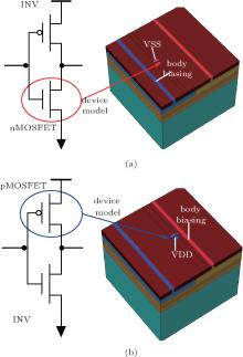
Due to the good look-inside capability, the three-dimensional TCAD simulation is widely used for investigating the mechanism of single-event charge collection.[12– 18] In this paper, we use the Sentaurus TCAD vE-2010.03 from Synopsys. Both the nMOSFET and pMOSFET are simulated. Figure 1 presents the simulated structure for the nMOSFET and pMOSFET respectively. There is a N+ deep implant with the peak of the Gaussian at 2× 1018 cm− 3 and depth of 600 nm. The studied transistor is modeled as the three-dimensional numerical model, and the other transistors are modeled as the SPICE mode. The three-dimensional numerical models are calibrated to match the current– voltage curves obtained from the commercial 65-nm CMOS process compact models.
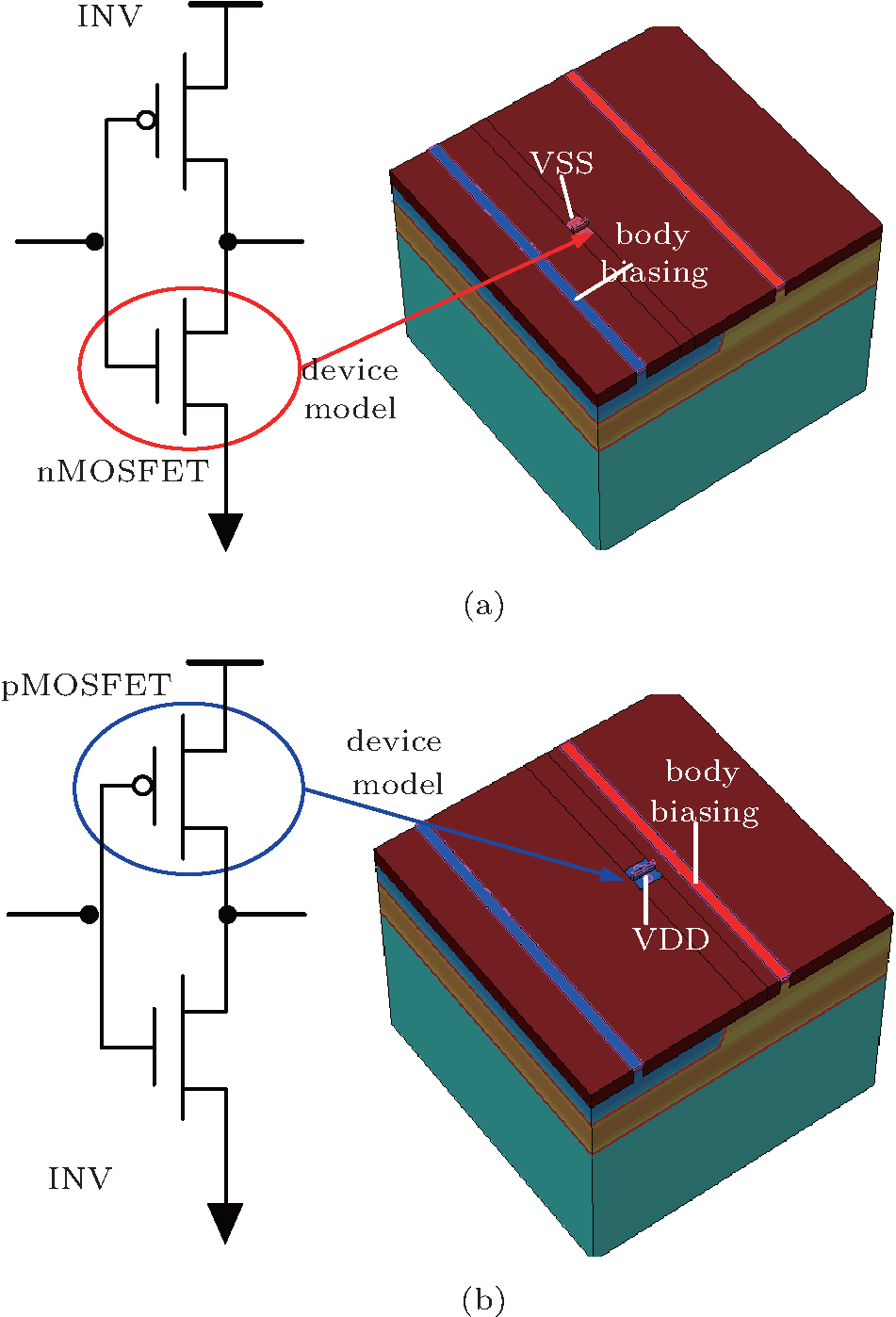 | Fig. 1. Simulated structure for this study. (a) nMOSFET, (b) pMOSFET. |
The size of the pMOSFET is W : L = 450 nm:60 nm, and the size of the nMOSFET is W : L = 300 nm:60 nm. The length of the source and drain of the transistors are both 0.2 μ m. The width of the n-well contact is 0.15 μ m.
In the simulated structure, the body biasing is applied on the well-contact. For the nMOSFET, the RBB is referred to as that the voltage of the body biasing is (VSS + Vbiasing), and the FBB is referred to as that the voltage of the body biasing is (VSS − Vbiasing). For the pMOSFET, the RBB is referred to as the voltage of body biasing is (VDD + Vbiasing), and the FBB is referred to as that the voltage of body biasing is (VDD – Vbiasing).
In this study, the FBB mode, RBB mode, and the normal mode are all studied. The supply voltage is set as 1.0 V.
For the pMOSFET study shown in Fig. 1(a), the input of the INV is tied to HIGH. For the normal case, the bias voltage is set as 1.0 V. For the FBB mode, the bias voltage is set as 0.4 V, 0.6 V, and 0.8 V. For the RBB mode, the bias voltage is set as 1.2 V, 1.4 V, and 1.6 V.
For the nMOSFET study shown in Fig. 1(b), the input of the INV is tied to LOW. For the normal case, the bias voltage is set as 0.0 V. For the FBB mode, the bias voltage is set as − 0.2 V, − 0.4 V, and − 0.6 V. For the RBB mode, the bias voltage is set as 0.2 V, 0.4 V, and 0.6 V.
During the simulation, the incident ion will strike the drain center of the studied transistor. The LET value is assumed to be constant along the heavy ion track. The length and radius of the ion track are 5 μ m and 0.05 μ m.
The following physical models are used: 1) Fermi– Dirac statistics; 2) band-gap narrowing effect; 3) doping-dependent SRH recombination and Auger recombination; 4) temperature, doping, electric field, and carrier-carrier-scattering impact on mobility; 5) incident heavy ions are modeled using a Gaussian radial profile with a characteristic 1/e radius of 50 nm and a Gaussian temporal profile with a characteristic decay time of 0.25 ps; and 6) a hydrodynamic model is used for carrier transportation. Unless otherwise specified, the default models and parameters provided by Sentaurus TCAD vE-2010.03 are used.
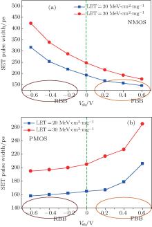
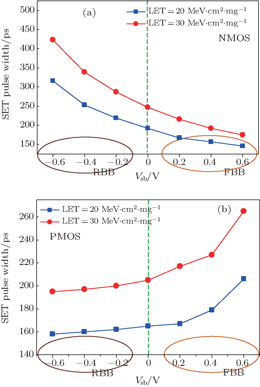
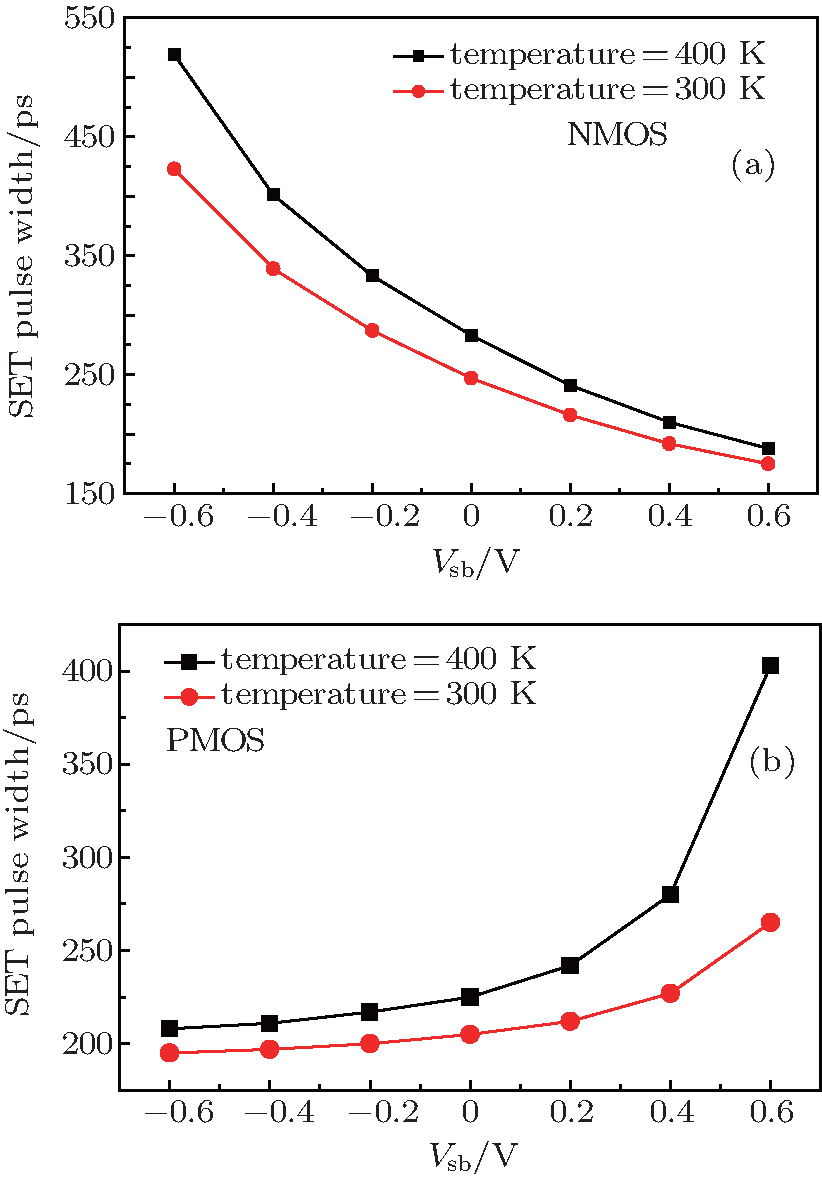
As the SET pulse width is closely related to the amount of charge collection, we monitor the SET pulse width at the output of the studied inverter to representthe charge collection amount under different body biasing cases. Figure 2 shows the simulation results as the incident LET is 20 MeV· cm2/mg and 30 MeV· cm2/mg. It can be observed that the effect of the body biasing on the charge collection is quite contrary for the nMOSFET and pMOSFET.
 | Fig. 2. Simulation results. (a) nMOSFET, (b) pMOSFET. |
For the nMOSFET, the RBB will have an adverse effect on the charge collection, and the FBB will reduce the charge collection. For the pMOSFET, the effect of RBB on the SET pulse width is small, while the FBB will increase the charge collection.
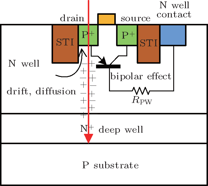
Previous researches have proved that the main charge collection mechanism for the pMOSFET in the deep N-well process is drift and diffusion and the mechanism for the nMOSFET is drift, diffusion and bipolar amplification effect as Vsb = 0 V.[12– 15] Figure 3 shows the comparison of source behavior in nMOSFET and pMOSFET for the deep N-well and twin well process as the Vsb = 0 V. It can be observed that the charge collection mechanism for the twin and deep N-well process is different. For the nMOSFET, the main charge collection mechanism in twin-well process is drift and diffusion, and the source will sink electrons. Whereas, the main charge collection mechanism in deep N-well process is drift, diffusion, and bipolar amplification effect, and the source will inject electrons. For the pMOSFET, the main charge collection mechanism in twin-well process is drift, diffusion and bipolar amplification effect, and the source will inject holes. Whereas, the main charge collection mechanism in deep N-well process is drift, diffusion, and the source will sink holes. This simulation results is consistent with the previous conclusion.[12– 14]
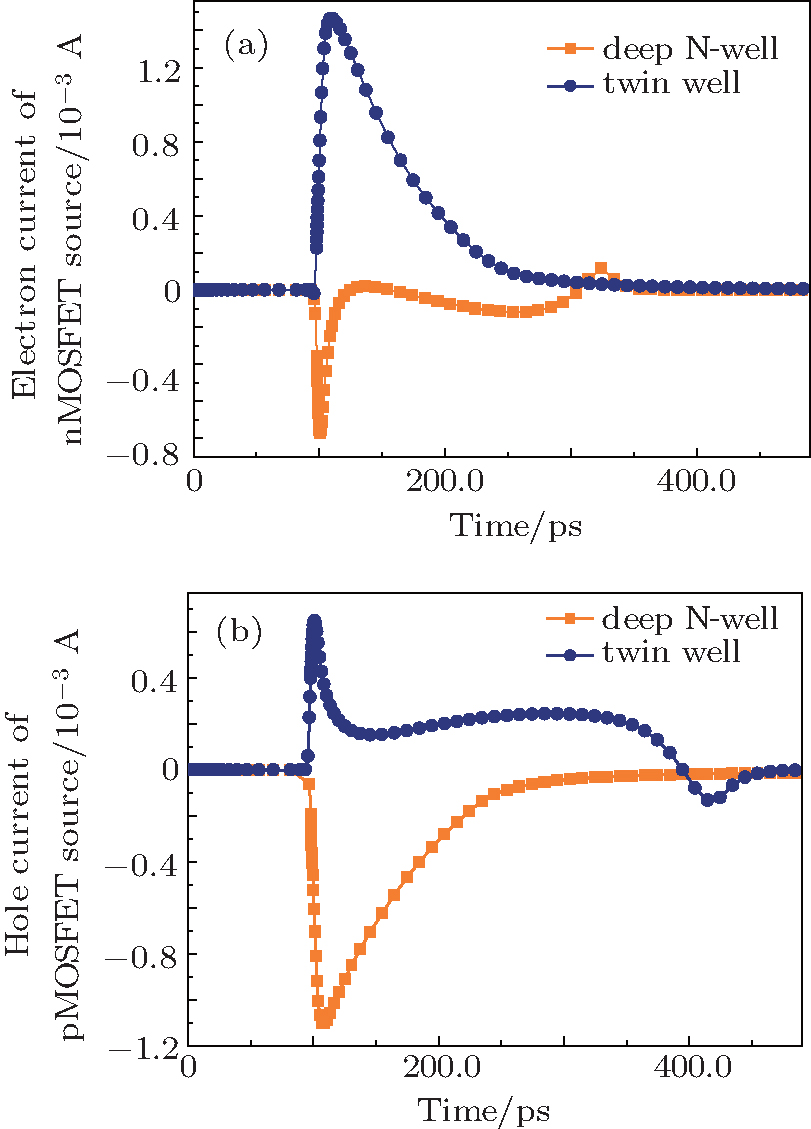 | Fig. 3. The source behavior of the pMOSFET and nMOSFET in deep N-well and twin well. (a) Electron current of nMOSFET source, (b) hole current of pMOSFET source. |
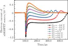
Figure 4 presents the electron current of nMOSFET source under different body biasing cases. In the normal case (Vsb = 0 V), the parasitic NPN shown in Fig. 5 is turned on as the ion strikes the drain. The source of nMOSFET will inject electron. This increases the charges collected by the drain. In the FBB mode, the voltage drop between the N-well and source junction is enhanced, and the conductance of the parasitic NPN decreases, causing the NPN turn off and the source collect electrons. However, in the RBB mode, the conductance of the parasitic NPN is increased. The parasitic bipolar amplification is enhanced. This causes the larger charge collection amount.
 | Fig. 4. Electron current of nMOSFET source under different body biasing cases. |
 | Fig. 5. Parasitic NPN in P well. |
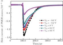
For the pMOSFET, figure 6 presents the relationship between the hole current of pMOSFET source and the body biasing voltage. In the normal case (Vsb = 0 V), the main charge collection mechanism of the pMOSFET in deep N-well is drift and diffusion. The source of the pMOSFET can help to sink the excess holes to reduce the charges collected by the drain. In the FBB mode, the parasitic PNP shown in Fig. 7 begins to form. The ability of the source to collect holes decreases. This increases the charges collected by the drain. When the FBB reaches some value, the parasitic PNP transistor can be even turned on.
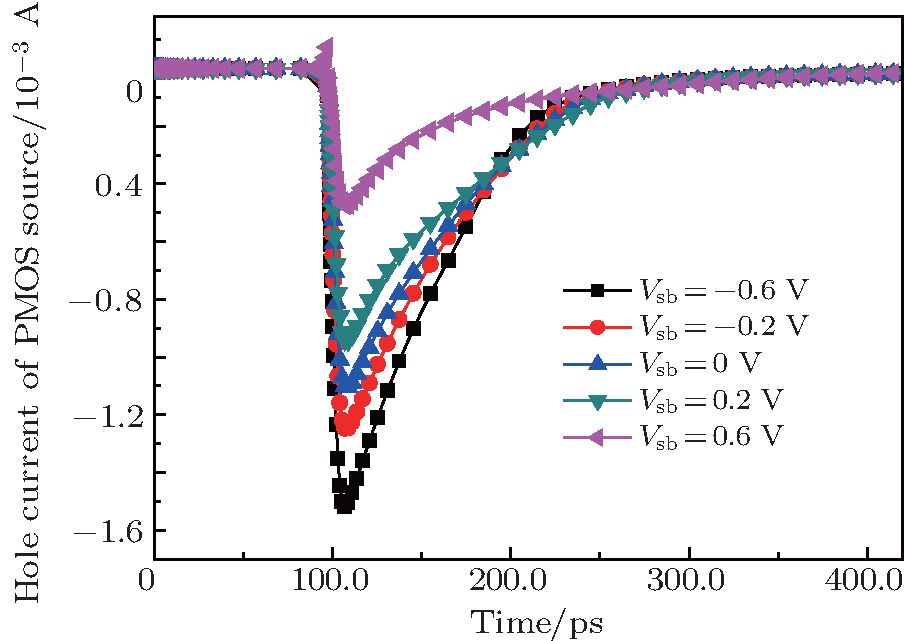 | Fig. 6. Hole current of pMOSFET source under different body biasing cases. |
 | Fig. 7. Parasitic PNP in N well. |
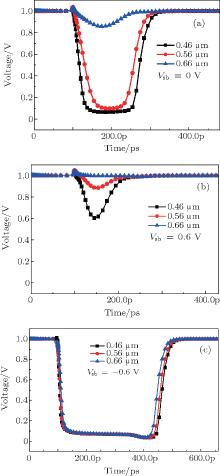
From the above analysis, we can conclude that the presence of the body biasing mainly affects the behavior of source. For the nMOSFET, the parasitic bipolar amplification is enhanced in RBB mode. This will affect the charge sharing effect. To demonstrate this, we simulate the SET width as the ion strike location is 0.46 μ m, 0.56 μ m, and 0.66 μ m away from the center the nMOSFET, respectively. Figure 8 presents the simulation results for the normal, FBB, and RBB mode. It can be observed that due to the increased parasitic bipolar amplification, the charge sharing effect of the MOSFET is enhanced in RBB mode.
 | Fig. 8. Charge sharing effect three different modes: (a) normal mode, (b) FBB mode, and (c) RBB mode. |
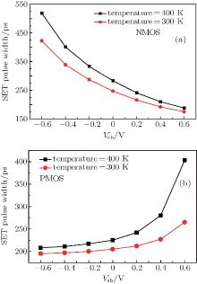
In this section, we simulate the SET pulse width under different temperatures and different body biasing. Figure 9 presents the simulation results for the nMOSFETand pMOSFET, respectively. It can be seen that the SET pulse width is larger for the higher temperature. For the nMOSFET, the bipolar amplification effect in the FBB mode is restrained. Thus, the increased SET pulse width is smaller than the one in RBB mode.
 | Fig. 9. Simulation results for the temperature case. (a) nMOSFET, (b) pMOSFET. |
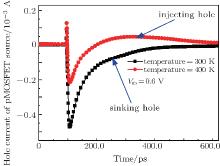
For the pMOSFET, bipolar amplification effect will be enhanced in FBB mode. From Fig. 9(b), it can be seen the difference for the SET pulse width at 300 K and 400 K is very large. We conclude that this is because that the parasitic PNP is turned on at 400 K. Figure 10 presents the hole current of pMOSFET source as Vsb = 0.6 V at 300 K and 400 K. It can be observed that the source will inject hole as the temperature is 400 K. This indicates that the parasitic PNP is turned on. The source just sinks holes as the temperature is 300 K.
 | Fig. 10. Hole current of pMOSFET source as Vsb is 0.6 V at 300 K and 400 K. |
Similar simulations are performed to analyze the effect of body biasing on the charge collection in twin-well process.
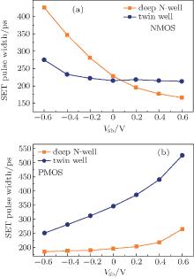
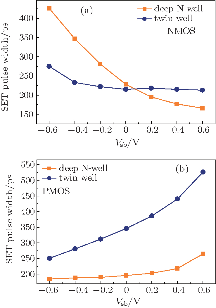
Figure 11 presents the comparison of the effect of body biasing on the SET pulse width in deep N-well and twin well process. Due to the different charge collection mechanism for the nMOSFET and pMOSFET in deep N-well and twin well, the effect of body biasing is different in these two processes.
 | Fig. 11. Comparison of the effect of body biasing on the SET pulse width in deep N-well and twin well process. (a) nMOSFET, (b) pMOSFET. |
For the nMOSFET in twin well, the main charge collection mechanism is drift and diffusion. As the FBB can only mitigate the bipolar amplification effect, the FBB has little effect on the SET pulse width for the nMOSFET in twin-well process. In deep N-well process, the main charge collection mechanism of nMOSFET is drift, diffusion, and bipolar amplification effect. As the FBB can mitigate the bipolar amplification effect, the SET pulse width is largely reduced in the BB mode for the nMOSFET in deep N-well process. For the pMOSFET in twin well, the main charge collection mechanism is drift, diffusion and bipolar amplification effect. As the RBB can mitigate the bipolar amplification effect, the RBB will largely attenuate the SET pulse width for the pMOSFET in twin-well process.
Using the three-dimensional technology computer-aided design (TCAD) numerical simulation, we evaluate the effect of the body biasing on the single-event charge collection in deep N-well technology. For the nMOSFET, the RBB will have an adverse effect on the charge collection, and the FBB will reduce the charge collection. For the pMOSFET, the effect of RBB on the SET pulse width is small, while the FBB will increase the charge collection. Our simulation results also show that the parasitic PNP might be turned on to increase the charge collection under FBB mode for the pMOSFET in deep N-well technology. Finally, we compare the effect of body biasing on the charge collection in deep N-well and twin well process.
| 1 |
|
| 2 |
|
| 3 |
|
| 4 |
|
| 5 |
|
| 6 |
|
| 7 |
|
| 8 |
|
| 9 |
|
| 10 |
|
| 11 |
|
| 12 |
|
| 13 |
|
| 14 |
|
| 15 |
|
| 16 |
|
| 17 |
|
| 18 |
|