


Characteristics of drain-modulated generation current in n-type metal-oxide-semiconductor field-effect transistor
[Chen Hai-Feng† , Guo Li-Xin, Zheng Pu-Yang, Dong Zhao, Zhang Qian]
, Guo Li-Xin, Zheng Pu-Yang, Dong Zhao, Zhang Qian]
|
|


†Corresponding author. E-mail: chenhaifeng@xupt.edu.cn
*Project supported by the National Natural Science Foundation of China (Grant No. 61306131) and the Research Project of Education Department of Shaanxi Province, China (Grant No. 2013JK1095).
Drain-modulated generation current IDMG induced by interface traps in an n-type metal-oxide-semiconductor field-effect transistor (nMOSFET) is investigated. The formation of IDMG ascribes to the change of the Si surface potential φs. This change makes the channel suffer transformation from the inversion state, depletion I state to depletion II state. The simulation result agrees with the experiment in the inversion and depletion I states. In the depletion II state, the theoretical curve goes into saturation, while the experimental curve drops quickly as VD increases. The reason for this unconformity is that the drain-to-gate voltage VDG lessens φs around the drain corner and controls the falling edge of the IDMG curve. The experiments of gate-modulated generation and recombination currents are also applied to verify the reasonability of the mechanism. Based on this mechanism, a theoretical model of the IDMG falling edge is set up in which IDMG has an exponential attenuation relation with VDG. Finally, the critical fitting coefficient t of the experimental curves is extracted. It is found that t = 80 mV = 3 kT/ q. This result fully shows the accuracy of the above mechanism.
The generation current in the metal-oxide-semiconductor field-effect transistor (MOSFET) is a leakage current that results from the interface traps which serve as the generation sites when the channel is in the non-equilibrium state.[1, 2] Since this type of current is closely related to the traps, it is widely used to detect the damage created by the hot carrier and the negative bias temperature instability (NBTI) stresses.[3– 5] Scoot et al. applied this current to study the radiation damage in x-ray imagers and proposed a new pixel design based on gated diode structures that will provide the improved image quality.[6] Our previous paper studied the degradation of MOSFET by the method of generation current transconductance, [7] then we discussed the effect of substrate bias on the generation current and recently set up a theoretical model for this current.[8, 9] In addition, the generation current was also involved in several researches about the fin field-effect transistor and its reliability issues.[10, 11]
All the generation currents used in the above studies are gate-modulated. This type of current can be measured by the method of sweeping the gate which makes the channel state change from accumulation, depletion to inversion. In the measurement, the drain bias VD is fixed to keep the quasi-Fermi level of the substrate minority carrier unchanged, and therefore it plays the role of maintaining the non-equilibrium state in the depletion region during the formation of gate-modulated generation current. However, VD is often varied in the work condition of MOSFET meaning that the non-equilibrium state is dynamic. Since the dynamic non-equilibrium state should affect the generation function of interface traps, a new important problem arises: what is the feature of the generation current under the dynamic non-equilibrium condition? It can also be expressed as: how does the drain modulate the generation current? Nonetheless, little attention has been paid to this problem so far.
On the basis of the above discussion, this paper aims to reveal the features of drain-modulated generation current IDMG and expound the deep physical mechanisms behind these features. The nMOSFET with a 4-nm gate oxide thickness was used in this paper. Through analyzing the changes of IDMG versus VD, their relationship and the related physical mechanisms are discussed deeply by combining experimental results with theoretical analysis.
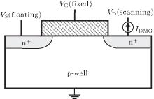
The device used in this paper was an nMOSFET with an n+ poly-Si gate fabricated by using 90-nm complementary-metal-oxide-semiconductor (CMOS) technology. The gate oxide thickness tox was 4 nm with width/length = 6 μ m/0.35 μ m. The threshold voltage of the device was 0.49 V. For the drain-modulated generation current measurement, floating the source and grounding the substrate, the drain was swept from − 0.2 V to 1.0 V. The gate bias VG was fixed at 0.1, 0.2, 0.3, 0.4, 0.5, 0.6, and 0.8 V. The drain current was IDMG. The schematic diagram of the IDMG measurement is shown in Fig. 1. All electrical tests were performed by using a Keithley 4200 precision semiconductor parameter analyzer. In addition, all the simulations were done using the MATLAB software.
 | Fig. 1. The schematic diagram of the drain modulated generation current IDMG measurement with nMOSFET. |
The IDMG is an interface trap-induced drain leakage current because of the Shockley– Read– Hall (SRH) effect. In the SRH model, the electron density ns and hole density ps at the interface Si/SiO2 can change the generation rate g. The relationship between them is[12]

where ns and ps can be written as

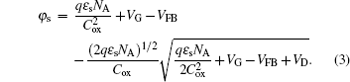
with n0 and p0 the substrate minority and majority carrier density, respectively, p0 = NA and β = kT/q, m is the adjustment coefficient for the practical device and m = 1 in the ideal situation, while φ s is the surface potential given by
When the substrate doping is not heavy, the first and fourth items in Eq. (3) are too small and can be ignored. Thus φ s is dominated by (VG– VFB). If VG > 0 V, φ s > 0 V because VFB is negative generally. The change of VD results in the change of ns at the given VG according to Eq. (2), which eventually causes g changes. Since VD is larger than 0, ns decreases with the increase in VD.
When ns ≥ p0, the channel Si surface is stepped into the inversion state, then a larger number of electrons make the interface traps lose their generation roles and g is zero. In this case, VD can be deduced according to the expression of ns in Eq. (2) as follows:

As VD increases, ns decreases which leads to the Si surface presenting the depletion state, then g should increase with the increase in VD.
When ns ≤ ni/5 that is one-tenth of 2ni, the change of ns has no effect on g. In this case, VD should be

For ps, it cannot affect g only if ps < = ni/5. According to Eq. (2), there is

so combining Eqs. (3) and (6), it is deduced as

which shows that VG should be very small or even negative in the case of ps = ni/5 under VFB < 0 V when p0 is not heavy. Hence, if VG is larger than this critical value, ps has no influence on g in theory. In a word, g should almost keep constant when the value of VD satisfies Eq. (5).
Figure 2(a) shows a schematic diagram of the relationship between VD and g. As VD increases with a given VG, g increases and the channel state changes from inversion to depletion. Moreover, the depletion divides into two depletion states: I state and II state. Figure 2(b) shows the simulated g versus VD curves under different given VG. It can be seen that the simulated g curve complies with the schematic diagram basically and the g curve shifts rightwards as VG increases with the reason that VG induces the change of φ s.
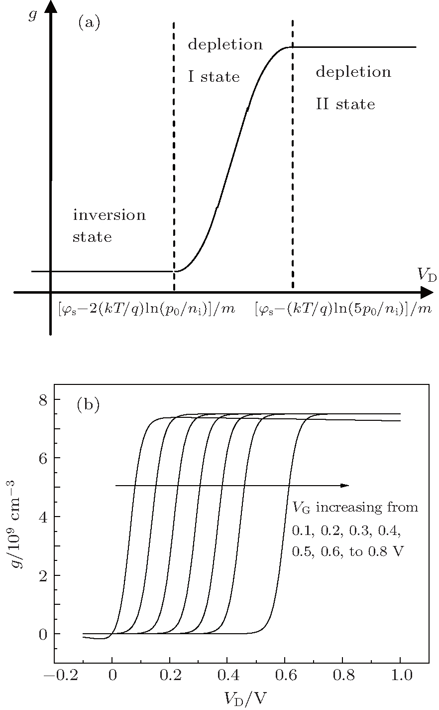 | Fig. 2. (a) A schematic diagram of the relationship between VD and g. (b) Curves of the simulated g versus VD. In the simulation, tox = 4 nm and p0 = NA = 4 × 1015 cm− 3, m = 1.25 and VFB = − 0.35 V. |
Since IDMG is in direct proportion to g, that is

where r = aqNitσ vth, a is the gate area, q is the single electron charge, Nit is the density of interface traps, σ is the cross section of a trap, and vth is the thermal velocity, the variation of the IDMG curve has the same trend as the g curve. Once VG is given, IDMG increases with VD increasing at first and afterwards steps into saturation in which IDMG cannot increase any more.
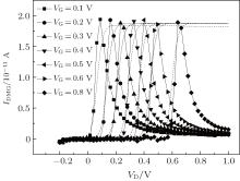
Figure 3 shows the experimental IDMG curves. For a given VG, the IDMG curve is almost zero at the beginning of VD increasing from − 0.2 V, then all of a sudden it augments. After exceeding its maximum, the curves start to drop with VD increasing and finally present a peak shape. It can be seen that the curves shift rightwards and the peaks almost keep constant as VG changes from 0.1 to 0.8 V. Figure 3 also shows the simulated IDMG curves based on g in the Fig. 2(b). Compared with the simulated curve, the experimental curve is basically consistent with it from the inversion to depletion I state.
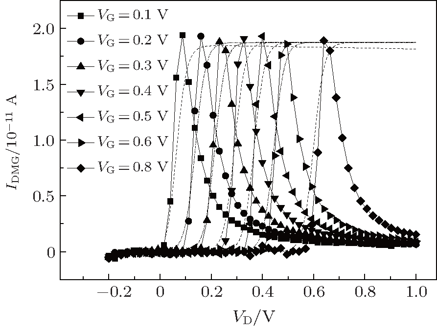 | Fig. 3. Comparison of the experimental IDMG (symbol line) and simulated IDMG (dash line) based on Fig. 2(b). Here, w/l = 6 μ m/0.35 μ m. Nit = 2 × 1011 cm− 2, and σ = 4 × 10− 13 cm− 2. Other structure parameters are the same as those in Fig. 2(b). |
In order to better confirm the validity of the theory in depletion I state, we analyze the peak point which is the boundary point of depletion I state. Because IDMG is proportional to g, g is the maximum at the IDMG peak. At this peak, ns = ni/5. It defines VGP and VDP as the VG and VD corresponding to the IDMG peak respectively. According to Eqs. (2) and (6), VGP and VDP have the following relationship:

Since the third and fourth items in Eq. (9) are too small and can be ignored when NA < 1016 cm− 3, equation (9) can be simplified as

Figure 4 shows the relationship between VGP and VDP extracted from the experimental curves in Fig. 3. It can be seen that VGP has a linear relationship with VDP. The fitted equation is: VGP = sVDP, where s = 1.24, which agrees with Eq. (10) and s is very close to the value of m (m = 1.25) in the simulated curves in Fig. 3. Hence, the agreement fully proves the validity of the theory about the depletion state mentioned above. However, the experimental curve in Fig. 3 after reaching the peak cannot step into saturation like the simulated curve, but drops quickly with VD increasing. This experimental result implies that the physical mechanism behind Fig. 2 does not hold in the depletion II state. Further, it can be deduced that the transport of interface generation current suffers some kind of inhibition after reaching the maximum value.
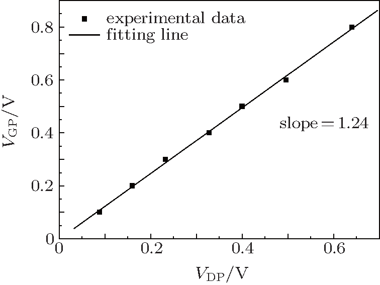 | Fig. 4. Relationship between VGP and VDP extracted from the experimental IDMG curves in Fig. 3. |
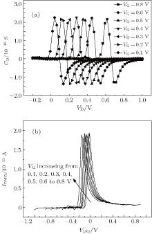
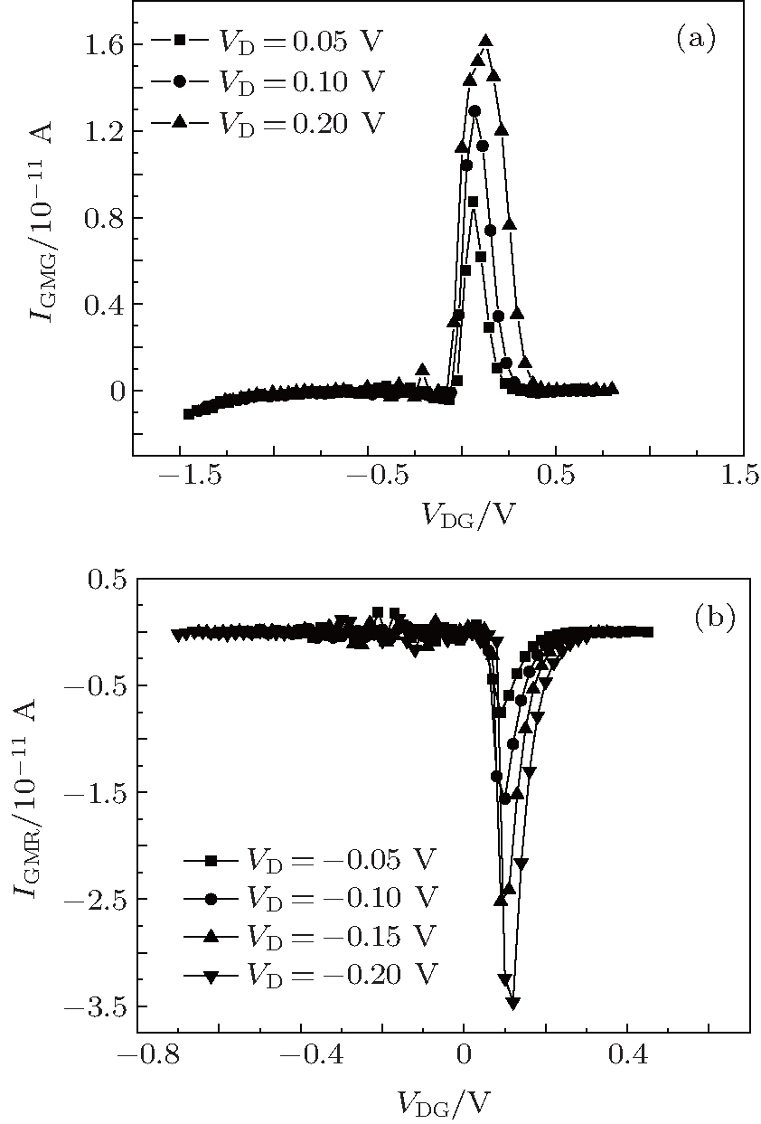
To seek the real physical mechanism hidden in the IDMG falling edge, figure 5(a) presents the conductance CD of experimental IDMG from Fig. 3. CD can indicate the ability of VD controlling IDMG. It can be seen that there are two CD peaks located in the rising edge and falling edge of IDMG, CDRP and CDFP, respectively. All the CDRP and CDFP keep constant in Fig. 5(a). Obviously, VG seems to have little influence on the CD curve and just shifts the CD curve rightwards. Namely, VG cannot affect the ability of VD controlling IDMG curves. Thus the problem of VD controlling the IDMG curve can be transformed into that of the drain-gate voltage VDG (VDG = VD− VG) controlling the IDMG curve. The benefit of this transformation is to compress the group of IDMG curves and to well make the implicit information present. Then, figure 5(b) presents the IDMG curves under VDG. VDG at the IDMG peak is defined as VDGP and then VDGP = VDP − VGP = (1/s − 1) VGP = − 0.2VGP. Since VGP is not beyond 0.8 V, the range of VDGP is very small. Therefore, the current peaks are located at about VDG ≈ 0 V. In Fig. 5(b), the left side of the curve corresponds to the rising edge of the IDMG versus VD curve, and the right side corresponds to the falling edge of the IDMG versus VD curve. Because the difference between the simulation and experimental results in Fig. 3 is mainly focused on the falling edge of the VD versus IDMG curve, it needs to focus on the right side of the IDMG versus VDG curve. Further, ignoring the slight shift of the current peak, a common feature in all the curves is that the curves drop under VDG > 0 V as VDG increases. To sum up, VDG controls the change of the falling edge of the experimental IDMG curve in Fig. 3.
 | Fig. 5. (a) Conductance of the curves from Fig. 3, and (b) variations of the experimental IDMG with VDG extracted from Fig. 3. |
Since VDG is the drain-to-gate voltage drop, it affects the Si surface of the channel around the drain. Hence, the whole channel is divided into two regions: main channel region A and region B that is around the drain, as shown in Fig. 6. The generation rates of these two regions are g1 and g2, respectively. At a given VG, the channel steps into depletion II state in Fig. 1 and the increase of VD almost cannot change g1. However, VDG should increase with VD increasing. As a consequence, the bending of the Si energy band at region B decreases and lessens the surface potential φ s. When ps > ni/5 in region B, g2 starts to decrease, as can be seen in Fig. 6(a). As VD continues to increase, the channel depletion region returns to region A completely and an accumulation state can be formed in region B, as shown in Fig. 6(b). So the generation function of the interface traps in region B is shielded and g2 is close to zero. The channel electrons created by the trap’ s generation are eventually collected by the drain. Based on the above discussion, the electron transport of the whole channel electron is subject to g2. Namely, g2 dominates the magnitude of the generation current. On the basis of the above discussion, g2 should lessen with VD increasing that is beyond VDP. Thus, the generation current decreases. As VD further increases, region B steps into the accumulation state, g2 becomes zero, and the generation current disappears. As can be seen from Fig. 3, the experimental curves in the depletion II state just conform to this logical deduction.
 | Fig. 6. Schematic diagrams of channel states as VD varies. (a) Depletion situation of B region, and (b) accumulation situation of B region. |
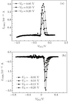
If the above theory of VDG controlling the falling edge of IDMG is reasonable, the generation current versus the VDG curve should obey it no matter which measurement method is used. Figure 7(a) shows the curve of gate-modulated generation current IGMG versus VDG, which is obtained by scanning VGwith fixing VD. It can be seen that the IGMG curve changes from rising to falling when VDG > 0 V. This phenomenon agrees with the case of IDMG, which considerably indicates that the theory suits IGMG. More, the curve of recombination current versus VDG should present the same shape as the IDMG curve because the recombination current also results from the SRH effect. Figure 7(b) shows the curve of the gate-modulated recombination current IGMR versus VDG under VD < 0 V. It can also be seen that the IGMR curve firstly goes up and then drops when VDG > 0 V. In general, the rationality of the theory is verified considerably by these two additional experiments above.
 | Fig. 7. (a) Variations of gate-modulated generation current (IGMG) with VDG, and (b) variations of gate-modulated recombination current (IGMR) with VDG. |
On the basis of the theory’ s rationality, the variation of IDMG in depletion II state is discussed in detail as follows. The gate-to-drain voltage drop VGD dominates φ s, the VG in Eq. (3) should be substituted by VGD. Due to VGD = − VDG, the surface potential around the drain corner φ SD is
Thus, ps is deduced as

which increases quickly after exceeding ni/5 and then ps ≫ ni and ns ≪ ni. Since ps plays the dominant role in the falling stage of IDMG, g2 is simplified as
As mentioned before, the first and fourth terms of Eq. (11) can be ignored, then substituting Eq. (11) into Eq. (13), g2 can be written as


In order to meet the practical devices, an additional accommodation-coefficient n is introduced in Eq. (14), then g2 becomes

which indicates that g2 decreases with VDG increasing when VG is given. According to Eq. (8), IDMG also shows the exponential decay relationship with VDG. Defining I0 = rb, the theoretical model of IDMG in the falling edge can be written as

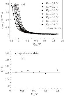
In order to verify the correctness of Eq. (17), figure 8(a) extracts the experimental IDMG curves at different fixed VG from Fig. 5(b) and fits them. The expression obtained by the curve fitting is given by

with c and t the fitting coefficients. The experimental model of Eq. (18) mainly has the same form as the theoretical model of Eq. (17), in which IDMG has the exponential attenuation relation with VDG. To further test the matching degree of the theory and experiment, figure 8(b) extracts the fitting coefficient t because t decides the degree of the exponential attenuation. As can be seen, t basically does not vary with the variation of VG, which is about 0.08 V or 80 mV. Since the thermal potential β = kT/q = 26 mV, t ≈ 3β . If n = 3 in Eq. (17), the decay degree with VDG of Eq. (18) becomes the same as that of Eq. (17). Hence, the value of t verifies the reasonability of the theoretical model of Eq. (17). Further, this result fully shows the accuracy of the mechanism of VDG controlling the falling edge of IDMG proposed in the above sections.
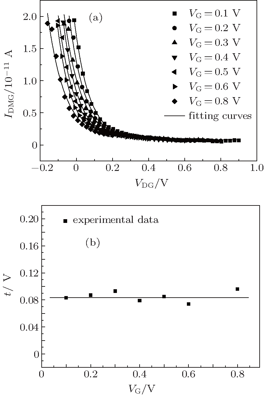 | Fig. 8. (a) The falling edges of experimental and fitted IDMG versus VDG curves, and (b) variations of t with VD extracted from panel (a). |
The characteristics of the drain-modulated generation current IDMG induced by interface traps in nMOSFETs are discussed. The change of VD induces the changes of φ s and thus changes ns and ps, which results in the formation of IDMG. During this formation, the channel suffers from the inversion state, depletion I state to depletion II state as VD increases with the given VG. The results of experiment and simulation agree well with each other in the inversion and depletion I states. However, the simulated curve keeps constant and the experimental curve drops quickly when the channel steps into the depletion II state. It is found that the falling edge of the experimental IDMG curve is close with the drain-to-gate voltage VDG. Since VDG affects the Si surface of the channel around the drain corner, the whole channel is divided into two regions: the main channel, region A, and region B, which is around the drain corner. The generation rate of region B is g2 dominating the generation current. VDG increases with VD increasing, which lessens φ s. Therefore, g2 increases and results in the drop of the IDMG curve. As VD further increases, region B is into the accumulation state and then the generation function of the interface trap is screened by a large number of holes. Consequently, IDMG disappears. The experiments of the gate-modulate generation and recombination currents are also applied to verify the reasonability of the above mechanism that is VDG controlling the falling edge of the IDMG curve. Based on this mechanism, a theoretical model is set up in which IDMG has the exponential attenuation relation with VDG. Finally, the fitting coefficient of the experimental curves t is extracted. It is found that t = 80 mV. These results fully show the accuracy of the above mechanism.
| 1 |
|
| 2 |
|
| 3 |
|
| 4 |
|
| 5 |
|
| 6 |
|
| 7 |
|
| 8 |
|
| 9 |
|
| 10 |
|
| 11 |
|
| 12 |
|