FePt nano-stripes fabricated on anodic aluminum oxide templates
[Deng Chen-Huaa), b) , Qiao Xin-Yua), b) , Wang Fang†a), b)  , Fan Jiu-Ping
a), b) , Zeng Haoc) , Xu Xiao-Hong‡a), b) ]
, Fan Jiu-Ping]
|
|

 , Fan Jiu-Ping
†Corresponding author. E-mail: wf_0716@163.com
‡Corresponding author. E-mail: xuxh@dns.sxnu.edu.cn
*
A new FePt nanostructure with stripe-like patterns has been prepared by direct current (DC) magnetron sputtering on anodic aluminum oxide (AAO) templates. AAO templates anodized under low voltages (7 V) demonstrate self-organized, maze-like patterns, different from the conventional porous structures obtained at high voltages. FePt thin films deposited on such templates tend to replicate the morphology of the templates. Although there is no obvious spatial ordering, the dimensions of the FePt nano-stripes are highly uniform, due to the constrained growth along the transverse direction of the AAO pattern. The magnetic properties are strongly influenced by this unique morphology. While continuous films demonstrate strong exchange coupling, the dominant interaction in FePt nano-stripes with the same nominal thickness is magnetostatic. The morphology also dictates the magnetization reversal behaviors, with thin films dominated by domain nucleation; while nano-stripes incline to reverse their magnetization by spin rotation. Our work demonstrates that self-organized AAO templates can be used to control the morphology and magnetic behavior of FePt materials.
FePt thin film materials are good candidates for strong permanent magnets and high density recording media due to their high anisotropy constant (Ku = 6.6 × 10⁷ erg/cm3) and excellent chemical stability.[1– 5] Nanostructuring can be used to influence their extrinsic magnetic properties by controlling their magnetization reversal processes, since the fundamental length scales relevant to magnetization reversal fall in the nanometer regime. So far, magnetic nanostructures with different morphologies have been fabricated and studied. For example, Albrecht et al.[6] obtained the Co/Pd curved surfaces by depositing on spherical nanoparticles which allow tailoring the orientation of the magnetic anisotropy by changing the deposition angle. Kim et al.[7] reported FePt nanodot arrays with perpendicular anisotropy grown by sputtering FePt films through ultra-thin anodic aluminum oxide (AAO) templates. Poudyal et al.[8] fabricated FePt nanorods and nanowires by chemical methods. To obtain hard magnetic properties, high temperature annealing is often required to obtain chemically ordered phases for many transition metal compounds. However, annealing at high temperatures can result in grain growth and drastic change in morphologies. Thus it is relatively difficult to fabricate hard magnetic nanostructures with controllable morphologies. Compared with other preparation methods for nanostructures, [5, 9– 11] AAO templates have many advantages, such as easily controllable dimensions, high thermal stability, facile and inexpensive preparation processes for large area arrays of self-organized nanostructures.[7, 12– 17] So far, FePt nanostructures with different morphologies such as nanodots, [7] nanowires, [12] nanotubes, [13] and antidots[14] have been fabricated using porous AAO templates. FePt thin films deposited on AAO tend to replicate the morphologies of the templates. For a typical voltage range, AAO forms hexagonally packed pore arrays, with the diameter and period of the pores dependent on the applied voltages and the electrolyte used. For a given electrolyte, both the diameter and period increase with the increase in voltage. However, if the applied voltage is too high, the walls of the pores become very thin and eventually collapse. When the applied voltage is below a threshold value for pore formation (∼ 10 V for sulfuric acid electrolyte), surface patterns with maze-like features can form rather than conventional porous arrays. While most research focuses on porous AAO templates, maze-like AAO templates and patterns grown on them have rarely been reported. A recent work[18] obtained interconnected maze-like FePt patterns on single crystalline MgO substrates. Such patterns originate from incomplete coverage of a thin film on a flat substrate, and are distinctly different from the largely discrete nano-stripes reported in the present work in terms of both their morphologies and magnetization reversal behaviors.
In this work, we report FePt nano-stripes grown on maze-like AAO templates fabricated at reduced anodization voltages. The structural and magnetic properties of the FePt nano-stripes with various thicknesses were studied. FePt films on glass substrates with identical nominal thicknesses were also presented for comparison. Due to the constrained growth along the transverse direction of the templates, the dimensions and morphologies of the FePt nano-stripes are highly uniform. Such morphologies have a strong influence on magnetic properties, especially for thinner films. In particular, the inter-granular exchange coupling was reduced, leading to more independent magnetization reversal of individual FePt nano-stripes.
The maze-like AAO templates were prepared by an anodization process.[19] A 99.99% aluminum foil was ultrasonicated in acetone, and then annealed at 500 ° C for 2 h in a vacuum. Before anodization the aluminum foil was polished in a 1:4 mixture of perchloric acid and ethanol. The anodization was carried out in 0.3 M sulfuric acid under constant voltages of 7 V for 5 h at 20 ° C. FePt films with varied thicknesses (5, 10, 15, 20 and 25 nm) were deposited on the maze-like AAO templates and on glass substrates by DC magnetron sputtering, respectively. The maximum thickness was chosen so that the maze-like feature of the AAO was replicated without significant aggregation. FePt films were deposited at an Ar gas pressure of 7.5 × 10− 3 Torr at room temperature with a base pressure lower than 6 × 10− 7 Torr. All samples were annealed at 600 ° C in a vacuum for 30 min to form the hard FePt phase. The morphology, composition, structural and magnetic properties of samples were characterized by high-resolution scanning electron microscopy (SEM), energy-dispersive x-ray spectrometry (EDS), x-ray diffraction (XRD), and superconducting quantum interference device (SQUID) magnetometer.
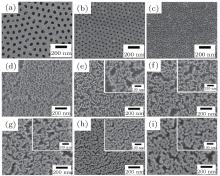
In the aluminum anodization process, the applied voltage is a key factor in determining the morphologies of the anodized alumina templates. Figures 1(a)– 1(c) show the surface morphologies of 20-nm FePt deposited on AAO template anodized under different voltages. For a typical voltage range, both the diameter and period decrease with voltage decreasing. When films are deposited on the templates, they can replicate the morphology of AAO. However, when the applied voltage is below the threshold value for pore formation (∼ 10 V), surface patterns with maze-like features can form rather than conventional porous arrays typically observed at higher voltages. When FePt thin films were deposited on such templates, they closely mimic the morphologies of the templates. Figures 1(d)– 1(i) show the surface morphologies of the maze-like AAO template when the anodization voltage is at a low value of 7 V and FePt material grown on them with various thicknesses. FePt layers with nominal thicknesses from 5 to 25 nm can all replicate the maze-like patterns of the AAO. The FePt nanostructures are characterized by nano-stripes with widths varying from 10 to 30 nm, for thicknesses of 5 to 25 nm, respectively. Their longitudinal dimensions also vary from 100 to a few hundred nm with thicknesses increasing. The nano-stripes are distributed uniformly and isolated from each other.
 | Fig. 1. The surface morphologies of 20-nm FePt deposited on AAO template anodized under (a) 40 V, (b) 25 V, and (c) 10 V. (d) Maze-like AAO template anodized under 7 V and [(e)– (i)] 5, 10, 15, 20, 25-nm FePt nanostripes grown on the AAO templates. The insets represent enlarged SEM images. |
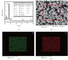
Figure 2(a) shows the typical EDS spectra of 25-nm-thick FePt nanostripes. It can be seen that Al and O elements are the main compositions in the sample, which come from the AAO template. Meanwhile, FePt can also be detected and the atomic ratio between Fe and Pt is about 1:1, which is the required condition to form the L10-FePt alloy phase. The high resolution back scattered electron (BSE) image of 25-nm FePt nanostripes and EDS elemental mapping images of Fe and Pt elements are shown in Figs. 2(b)– 2(d), respectively. Both the BSE image and the corresponding elemental mapping images show uniform brightness, which means that Fe and Pt elements on the AAO template form an alloy with uniform distribution of the two elements, and there is no phase separation.
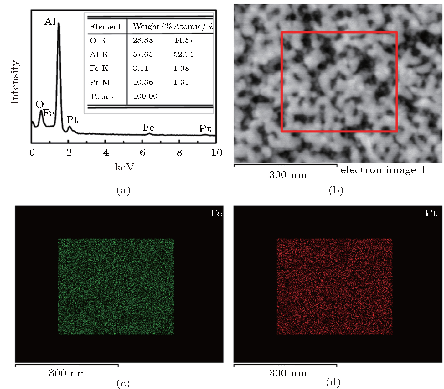 | Fig. 2. (a) The typical EDS spectrums of 25-nm FePt nanostripes. (b) The high resolution back scattered electron image of 25-nm FePt nanostripes. The elemental mapping images of (c) Fe (the green dots) and (d) Pt (the red dots) elements corresponding to the red square area of panel (b). |
To obtain a magnetically hard phase, the as-deposited FePt needs thermal annealing at high temperatures to realize the phase transformation from chemically disordered A1 phase to ordered L10 phase. For films on flat substrates, during such processes the FePt grains may grow and aggregate, leading to enhanced exchange coupling. For our nanostructures, due to the separation of the maze-like features of the template, the grain growth and coalescence of the FePt nano-stripes along the transverse direction will be hindered, and the grain size of FePt on AAO templates is typically smaller compared with FePt on other substrates[20, 21] under the same processing conditions. Therefore, the uniform stripes with small dimensions can be retained and are isolated from each other up to a certain thickness.
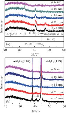
The XRD patterns of various FePt film thickness on glass substrates and on AAO templates are shown in Figs. 3(a) and 3(b), respectively. For FePt on glass substrates, the peaks of FePt (001) (2θ = 23.8° ), (110) (2θ = 32.4° ), (111) (2θ = 40.6° ), and (200 + 002) (2θ = 47.6° ) are observed with the film thickness increasing, which indicated the samples are randomly oriented. The peak at 47.6° is not the (200) (2θ = 46.5° ) or the (002) (2θ = 48.7° ) peak, it may be a mixture of the (200) and (002) peaks. While FePt on AAO templates only exhibited a (111) peak. The sharp peaks at 38° and 44° , come from the (110) and (113) peaks of the crystalline α -Al2O3 of the annealed AAO template, respectively. For all samples, the reflection from the L10 FePt (111) planes increase with FePt thickness increasing. After annealing at proper temperatures, the as-deposited FePt film will undergo a structural phase transformation from a disordered fcc structure to a chemically ordered fct structure. The phase transformation is evidenced by the emergence of superlattice peaks such as (001), (110), and (002).
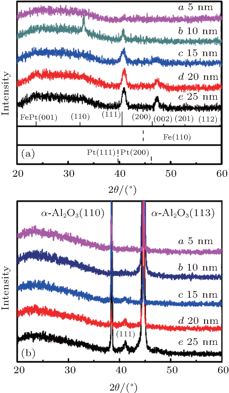 | Fig. 3. The XRD patterns of FePt films with different thicknesses (a) on glass substrates and (b) on AAO templates. The black vertical solid lines in panel (a) are the standard reflection peaks of the FePt alloy. The black vertical dash lines and dash dot lines in panel (a) are the standard reflection peaks of the (bcc) Fe and (fcc) Pt, respectively. |
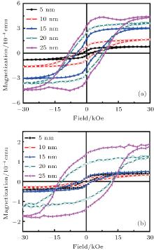
The magnetic properties of FePt are closely related to the film thickness whether deposited on AAOs or on glass substrates. Figure 4 shows the room temperature magnetic hysteresis loops of the annealed FePt on AAO templates and on glass substrates with thicknesses of 5, 10, 15, 20, and 25 nm, respectively, when the external magnetic field is in the plane. It is found that as the thickness increases from 5 to 25 nm, the coercivity (Hc) increases monotonically for both types of samples. This trend may result from the increase in the degree of L10 chemical ordering with increasing thickness.[20, 21] Lim et al.[22] reported that the ordering parameter decreases from 0.8 to 0.5 as FePt film thickness decreases from 40 to 10 nm. It is reasonable that as the lateral dimension of the nanostripes decreases, the ordering parameters decrease as well, even though this dimension is over many lattice spacings. It is possible that in addition to diffusion, reduced coordination numbers and other defects at the surface also tend to decrease the chemical ordering. Meanwhile, the thinnest samples have small average grain sizes (with lateral size < 10 nm and a thickness of 5 nm); and those grains with sizes smaller than the average values may exhibit superparamagnetism, leading to low Hc.
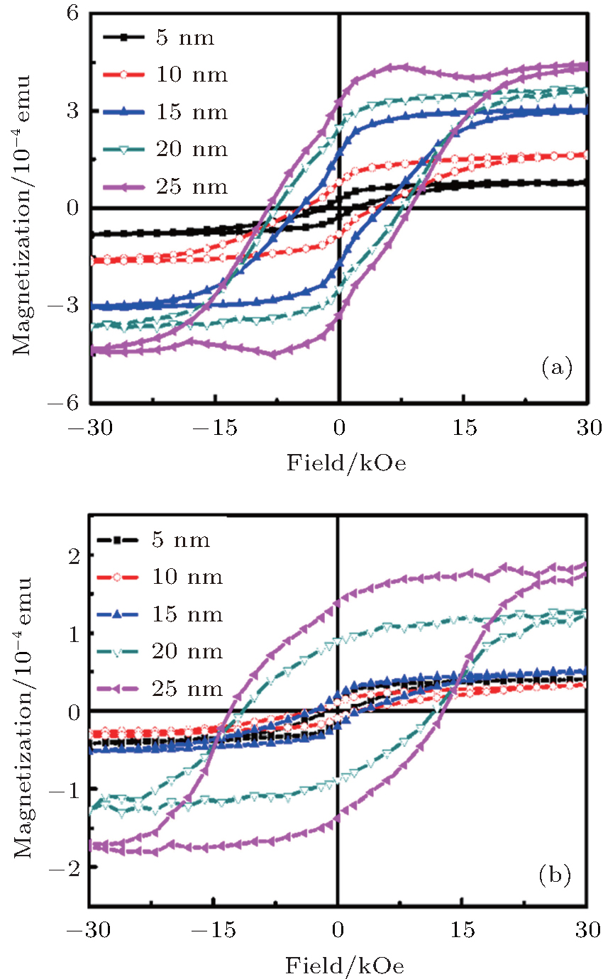 | Fig. 4. Magnetic hysteresis loops of the annealed FePt (a) on AAO templates and (b) on glass substrates with thicknesses of 5, 10, 15, 20, and 25-nm with the field in the plane. |
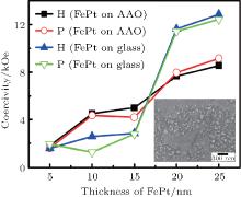
Figure 5 compares the out-of-plane (P) and in-plane (H) coercivity of FePt with different thicknesses deposited on AAOs and on glass substrates, respectively. The coercivity along both orientations for FePt deposited on AAO templates are generally larger than that on glass substrates, as the thickness is smaller than 15 nm. The larger Hc for films grown on AAO than that on glass substrates at small thicknesses can be attributed to different magnetization reversal mechanisms resulting from different morphologies of the two types of samples. Due to the maze-like feature of the templates, the growth and aggregation of FePt stripes along the transverse direction is suppressed during annealing, which can weaken the inter-granular exchange interactions. This can lead to more independent magnetization reversal of the grains by spin rotation, while the grains on glass substrates[23] may grow much larger and are strongly exchange-coupled. Thus the magnetization reversal is dominated by domain wall motion. It is noted that the trend is reversed when the thickness is over 15 nm. Once the thickness increases, the influence from the substrates is reduced and even FePt nano-stripes tend to grow and aggregate. Thus both types of samples can share similar magnetization reversal behavior. However, for thick, continuous films, the atoms can diffuse easily along all directions, which can enhance the degree of L10 chemical ordering; while for films on AAO templates, the diffusion is restricted to be along the longitudinal direction and thus can result in a lower degree of chemical ordering. In addition, the restricted growth in the transverse direction of the nanostripes also increases the surface area with missing nearest neighbors and other defects which tend to lower the chemical ordering. Thus Hc of FePt on glass substrates can exceed the values of FePt on AAO templates when the thickness is over 15 nm. One may note that the Hc values of the two samples with a nominal thickness of 5 nm are similar. From the inset of Fig. 5, we can see that 5-nm FePt on glass substrate shows island-like features with isolated particles. This morphology results in spin rotation-type magnetization reversal, similar to that on AAO. Because the deposited FePt on AAOs and on glass substrates are randomly oriented, the out-of-plane and in-plane coercivities show similar values.
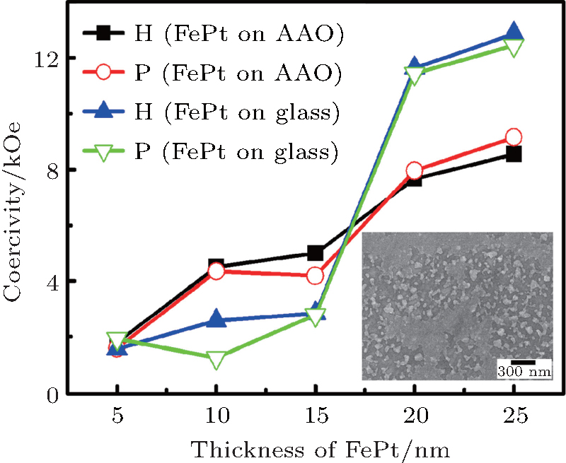 | Fig. 5. The out-of-plane (P) and in-plane (H) coercivity of FePt with different thicknesses deposited on AAOs and on glass substrates, respectively. The inset is the morphology of 5-nm FePt on glass substrate. |
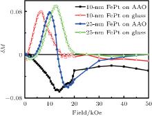
To confirm the postulated physical picture of the magnetization reversal, we further use δ M curves[24] and virgin curves to characterize the interactions and magnetization reversal behavior for the two types of samples. δ M = Md(H)/Mr(∞ ) − [1 − 2Mr(H)/Mr(∞ )], where Md (H), Mr (H), and Mr (∞ ) are the dc demagnetization, isothermal remanence, and saturation remanence, respectively. Typically, a positive peak in the δ M(H) curve is expected for exchange coupling and negative for magnetostatic interactions. As can be seen from Fig. 6, the δ M curve shows a negative peak for 10-nm-thick FePt nano-stripes, suggesting the dominating interaction is magnetostatic. This is consistent with the SEM images showing well-isolated patterns. While the FePt film on a glass substrate with identical thickness indicates strong exchange coupling, as evidenced by the positive δ M peak. For FePt deposited on both AAO templates and glass substrates, the exchange coupling increases with thickness increasing. It is noted that 25-nm-thick FePt on a maze-like AAO template shows two peaks: a positive and a negative one; while for the film with identical thickness, only a positive peak is observed. This further confirms that FePt nano-stripes possess weaker exchange coupling than films with identical thicknesses, even though their exchange interaction is enhanced with thickness increasing as well.
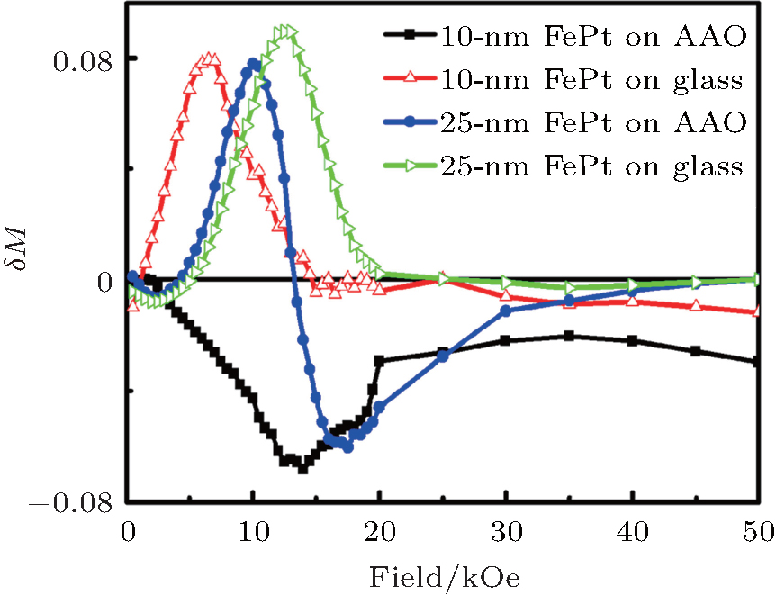 | Fig. 6. The δ M (H) curves of 10-nm and 25-nm FePt deposited on AAO templates and on glass substrates. |
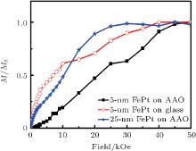
The isolated patterns together with reduced exchange coupling are expected to favor spin rotation over domain wall motion for FePt nano-stripes. This can be seen clearly when comparing the virgin curves of 5-nm FePt on the AAO template and on the glass substrate (Fig. 7). For nano-stripes, the virgin curve shows that magnetization first increases with field increasing at a lower rate; the rate then increases with field increasing. This is typically seen for samples showing spin rotation-type of magnetization reversal for single-domain particles. While for the 5-nm FePt film, the magnetization first rapidly increases with field increasing, then the rate slows down with further increasing field. This shows that the magnetization reversal is dominated by domain nucleation. When film thickness increases to 25 nm, the inter-granular exchange coupling sets in even for the nano-stripes, as seen in Fig. 6. This leads to the change of reversal mechanism from spin rotation to domain nucleation, as can be seen from Fig. 7.
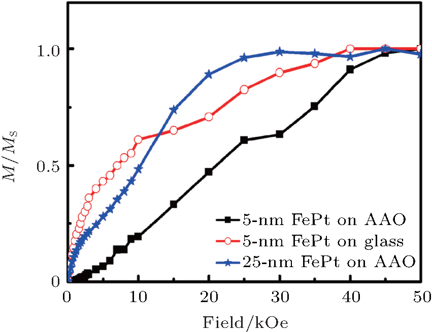 | Fig. 7. The virgin curves of 5 nm (squares), 25 nm (pentagons) FePt deposited on AAO templates and 5 nm (circles) FePt on glass substrate. |
We have developed a new FePt nanostructure with stripe-like patterns using AAO templates anodized at low voltages. The magnetic properties were strongly influenced by the morphologies dictated by the underlying templates. Due to the constrained growth along the transverse direction of the nano-stripes, the inter-granular exchange interactions are significantly reduced compared to continuous films. For thickness smaller than 15 nm, the magnetization reversal of the nano-stripes proceeds by spin rotation, which is different from FePt on glass substrates that reverse their magnetization by domain nucleation. This leads to larger coercivity of the FePt nano-stripes. With thickness increasing, the nano-stripes start to grow and aggregate, leading to exchange coupling and magnetization reversal modes dominated by domain nucleation.
| 1 |
|
| 2 |
|
| 3 |
|
| 4 |
|
| 5 |
|
| 6 |
|
| 7 |
|
| 8 |
|
| 9 |
|
| 10 |
|
| 11 |
|
| 12 |
|
| 13 |
|
| 14 |
|
| 15 |
|
| 16 |
|
| 17 |
|
| 18 |
|
| 19 |
|
| 20 |
|
| 21 |
|
| 22 |
|
| 23 |
|
| 24 |
|