

Optimization of intergrain connection in high-temperature superconductor Bi2Sr2CaCu2O x
[Li Cheng-Shan, Zhang Sheng-Nan† , Hao Qing-Bin, Ma Xiao-Bo, Lu Tian-Ni, Zhang Ping-Xiang]
, Hao Qing-Bin, Ma Xiao-Bo, Lu Tian-Ni, Zhang Ping-Xiang]
|
|


†Corresponding author. E-mail: snzhang@c-nin.com
*Project supported by the National Basic Research Program of China (Grant No. 2011CBA00104), the National Natural Science Foundation of China (Grant No. 51472206), the ITER Project of China (Grant No. 2013GB110001), and the Program for Innovative Research Team in Shaanxi Province, China (Grant No. 2013KCT-07).
A modified spark plasma sintering (SPS) technique was developed for the fabrication of Bi2Sr2CaCu2O x (Bi-2212) superconducting bulks with better intergrain connections. The influences of the modified SPS process on the microstructures, intergrain connections, and related superconducting properties were systematically analyzed. The modified SPS process can not only increase the final density of the bulk samples but also enhance the texture structures. Clean grain boundaries were obtained instead of the intergrain amorphous layers. Therefore the intergranular properties were obviously improved. Due to the better intergrain connections and the stronger flux pinning properties, the critical current densities of the Bi-2212 bulks obtained via the modified SPS process were greatly increased. The obtained improvements imply the possibility for the modified SPS technique to be used for enhancing the superconducting properties of the Bi-2212 tapes.
As an important high-temperature superconductor (HTS), Bi2Sr2CaCu2Ox (Bi-2212) exhibits excellent properties under low temperature and high magnetic field, including a high irreversible field Hirr of over 100 T and a large critical current density of ∼ 266 A· mm− 2 under high magnetic field (45 T).[1, 2] Besides, Bi-2212 is the only HTS material which can be made into isotropic round wires to simplify the winding process for magnet fabrication. Therefore it has great potential for the applications in high field magnets and large current applications.[3– 7] However, there are two factors that limit the transport properties of Bi-2212-based superconductors. One is the weak pinning mechanism, which can be attributed to its intrinsic lattice structure.[8] The introduction of pinning centers and modification of lattice structures can effectively enhance the pinning mechanism.[8– 12] The other factor is the intergrain weak links due to the low texture degree, [12– 15] high porosity, [16– 19] and/or grain boundaries with secondary phases or amorphous layers.[20, 21] Therefore, new techniques are needed in order to obtain Bi-2212 superconductors with aligned microstructures, higher density, cleaner grain boundaries, and stronger flux pinning properties for the practical applications.
Spark plasma sintering (SPS), also known as the field assisted sintering technique, has been widely used for the densification of ceramics and alloys.[22] Compared with the traditional sintering or hot pressing technique, SPS exhibits many advantages, such as fast heating rate, low sintering temperature, short sintering time, and high efficiency, and it is more environmentally friendly compared with other sintering techniques.[23] Besides, during the SPS process, the heat generation is internal, thus the sparks tend to appear first at the contact point between particles, which can not only ensure the high density of the bulk samples, but also improve the crystallization at the grain boundaries. Therefore, SPS has now been applied in the fabrication of many functional materials, including the functional gradient materials, [24] thermoelectric materials, [25, 26] ferroelectric materials, [27] and amorphous alloys.[28] It has also been applied in the fabrication of superconducting materials, such as YBCO thick films[29] and MgB2 bulk samples and tapes.[30] Aldica et al. developed a two-temperature route for the SPS synthesis of MgB2, and obtained bulk samples with the density of over 98% and strong flux pinning properties.[31] Suo et al. studied the effect of SPS on MgB2/Fe tapes. The higher Jc obtained by the SPS process can be attributed to the denser core and better crystallization of MgB2.[32]
In this study, SPS was applied on Bi-2212 to obtain superconducting bulk samples with high density. Meanwhile, in order to obtain the bulk samples with better textures, the SPS process was modified. Instead of packing the precursor powders directly into the graphite die for SPS, cold pressed pellets with smaller diameters were adopted as the starting materials for SPS. Thus, the pellets were not only condensed along the axial direction, but also expanded along the radial direction during the SPS process, which should be beneficial for the formation of texture structures. The influences of different fabrication processes on the microstructures, intergrain connections, and related superconducting properties were systematically investigated.
Bi2Sr2CaCu2O8+ δ precursor powders were synthesized by a modified co-precipitation process[33] with the starting materials of Bi2O3, SrCO3, CaCO3, and CuO (> 99.9%, all provided by Sinopharm Chemical Reagent Co., Ltd). A series of calcination processes in air at 800 ° C for 12 h, 820 ° C for 20 h, and 850 ° C for 20 h with intermediate grinding were performed to obtain the precursor powders with high Bi-2212 phase content. Bi-2212 bulk samples were fabricated with three different methods. The first bulk was fabricated by solid state synthesis. The precursor powders were cold pressed into a ϕ 20 mm pellet with the thickness of 1.5 mm under the pressure of 18 MPa for 10 min. Then the pellet was sintered at 865 ° C for 24 h (CP + sintering sample). The other two samples were both fabricated by the spark plasma sintering process. The SPS sample with diameter of ϕ 12.7 mm and thickness of 1.5 mm was obtained by packing the precursor powders directly into the graphite die and sintering at the temperature of 700 ° C for 5 min under the pressure of 60 MPa. For the modified SPS sample, the precursor powders were first cold pressed into a ϕ 10 mm pellet. Then the pellet was put at the center of the graphite die with diameter of ϕ 12.7 mm for SPS. The same sintering parameters were used, and the pellet with diameter of ϕ 12.7 mm and thickness of ∼ 1.5 mm was obtained. Due to the vacuum atmosphere involved during the SPS process, the samples sintered with SPS process were annealed in oxygen for 24 h in order to achieve their optimal superconducting properties.
Polycrystalline x-ray diffraction (XRD) patterns of both powders and bulk samples were taken by an x-ray diffractometer (Bruker D8 Advance) with Cu Kα radiation (λ = 0.15406 nm). The texture degrees of the (00l) peaks were used to evaluate the quality of the texture structures, which were estimated with the formula

where I00l represents the intensity of the (00l) peak for Bi-2212 phase, ∑ I2212 is the total diffraction intensity of Bi-2212, and ∑ Isp is the total diffraction intensity of the other secondary phases, including Bi2Sr2CuO6 (Bi-2201), alkali earth cuprates (AEC), Cu-free phase (CF), etc. Transmission electron microscopy (TEM) samples were prepared by grinding dimpling and ion milling (Gatan PIPS). The high-resolution transmission electron microscopy (HRTEM) was performed on a JEOL JEM-2010 microscope. The scanning electron microscopy (SEM) images were obtained with JEOL JSM-6700F. The densities of the bulk samples were measured using the standard Archimedes method. The AC susceptibility was measured by a superconducting quantum interference device (SQUID, MPMS-XL-7) with the AC magnetic fields of 0.1 Oe, 0.5 Oe, 1.0 Oe, and 1.5 Oe at frequency 333 Hz from 4.2 K to 120 K. Meanwhile, the SQUID was also used to measure the magnetization at the background temperature of 4.2 K. The bean model was adopted for the calculation of the critical current density Jc[34]

where a and b are the length and the width of the single crystal, respectively, and Δ M is the difference between the magnetization values with increasing field M+ and decreasing field M− at the same magnetic field.
The densities of the bulk samples fabricated by different methods are listed in Table 1. The density increases from 4.66 g/cm3 for the CP + sintering sample to 6.30 g/cm3 and 6.49 g/cm3 for the SPS and the modified SPS samples. Therefore, the porosities of the two SPS samples are only 5.7% and 2.9%, respectively. These data prove that the Bi-2212 bulks with higher density can be obtained by SPS processes.
| Table 1. Microstructural and physical parameters of the Bi-2212 bulk samples. |
Figure 1 shows the XRD patterns obtained for the precursor powders and the bulk samples fabricated by different methods. All the patterns can be indexed into the orthorhombic Bi-2212 structure (JCPDS No. # 46-0431). Comparing with the pattern of the precursor powders, the formation of the (00l) textural structure in the bulks can be noticed. The texture degrees of the bulk samples are calculated with Eq. (1) and listed in Table 1. The texture degree increases from 44.9% for the CP + sintering sample to 60.2% for the SPS sample. By adopting the modified SPS process, the texture degree is further improved to 65.3%, which proves the effectiveness of the modified SPS method on the preparation of highly textured bulk samples.
 | Fig. 1. XRD patterns of Bi-2212 precursor powders and bulks fabricated by different methods. |
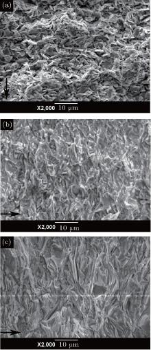
SEM images were taken on the fracture surfaces of the bulk samples. As shown in Fig. 2(a), in the CP + sintering bulk, random distribution of the particles can still be observed with lots of pores, which indicates the low density and low texture structure. After the SPS process, as shown in Fig. 2(b), a textural structure with particles aligning perpendicular to the pressing direction can be observed. The particles are well sintered together, although the applied sintering temperature is much lower than that of the CP + sintering bulk. During the modified SPS process, the bulks not only become thinner and denser, but also grow wider (from ϕ 10.0 mm to ϕ 12.7 mm). There is more space left for the growth of Bi-2212 plate-like grains along their ab plane. Therefore, obvious growth of particles along the radial direction can be observed in the modified SPS sample, as shown in Fig. 2(c). The average particle size Rg is estimated to be about twice as large as that of the SPS sample, as listed in Table 1. The decrease of porosity can also be noticed in these images.
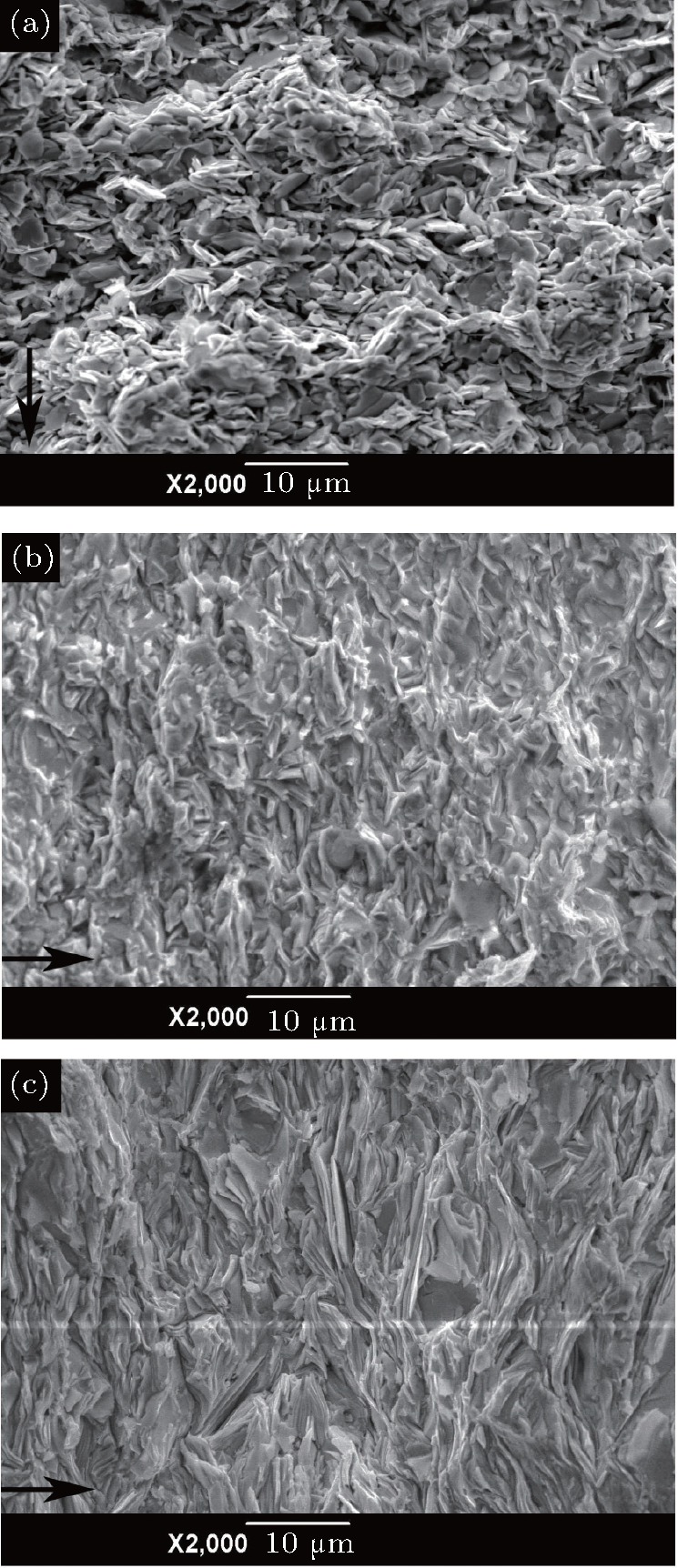 | Fig. 2. Fractal surface images of Bi-2212 bulks fabricated with (a) CP + sintering, (b) SPS, (c) modified SPS processes. The arrow points to the pressing direction. |
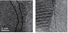
The changes of both density and texture structure have great influences on the intergrain connections. Therefore, in order to study the effect of different fabrication methods on the intergrain connections of the final bulk samples, HRTEM images were taken on the CP + sintering sample and the modified SPS sample, respectively. During the HRTEM observation, great differences were noticed at the grain boundaries of the samples. Amorphous components with the average thickness of ∼ 2 nm were observed within most of the grain boundaries in the CP + sintering bulk, the typical grain boundary image is shown in Fig. 3(a). The grain boundaries in the modified SPS bulk exhibited a much better crystallized structure, as shown in Fig. 3(b). Due to the highly textured structure, most of the grain boundary angles are 2° – 4° , which has no obvious influence on the current transportation.
 | Fig. 3. Typical HRTEM images for grain boundaries in (a) CP + sintering sample and (b) modified SPS sample. |
The AC susceptibility is widely used as a nondestructive method for the determination and characterization of the intergrain component in the polycrystalline high temperature superconductors. The imaginary component of the AC susceptibility is widely used to probe the nature of weak links in the polycrystalline superconductors.[33– 38]
The temperature dependence of the AC susceptibility of the Bi-2212 bulk samples obtained with different fabrication techniques is shown in Fig. 4. It can be observed that the real part of the AC susceptibility, χ ′ , of all the samples shows two drops. The first drop at Tc is due to the superconducting transition within grains, which changes from Tc ∼ 82 K for the CP + sintering bulk to ∼ 85 K for the two SPS bulk samples. The change of Tc can be attributed to the different oxygen contents resulting from the different fabrication methods. The second drop at TcJ is due to the occurrence of the superconducting coupling between grains, while on each of the imaginary part (χ ″ ) curves, a peak, which is a measure of the dissipation in the sample, can be observed. With the increase of AC field Hac, the peak shifts towards lower temperature and broadens. The peak temperature, Tp, of each bulk is plotted with the change of Hac in Fig. 4(d). It can be observed that the maximum Tp is obtained in the modified SPS bulk, and the CP + sintering bulk shows the lowest Tp. This suggests the better intergrain connection in the modified SPS sample.
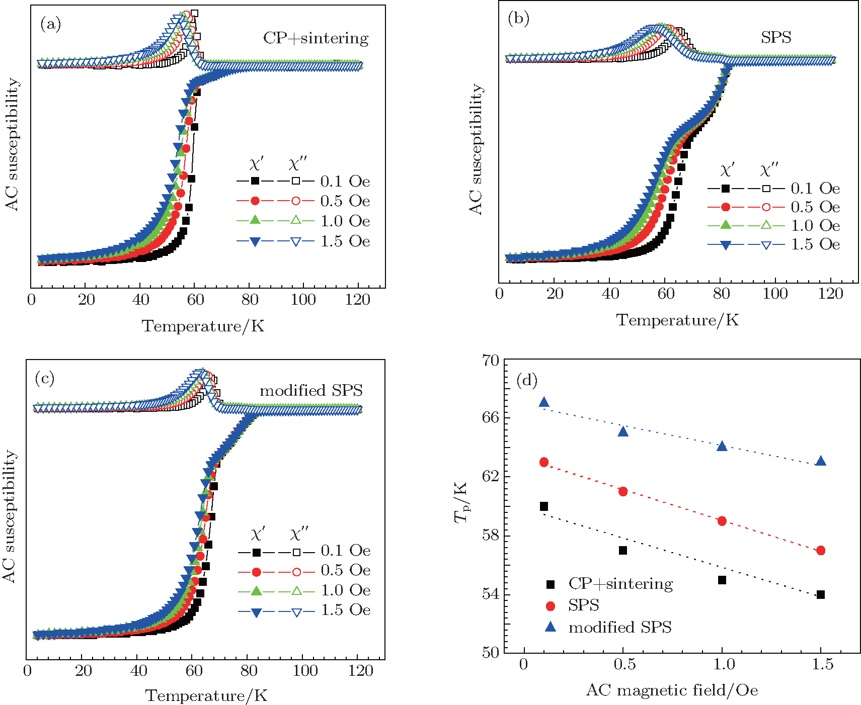 | Fig. 4. Temperature dependence of the AC susceptibility for Bi-2212 bulks fabricated by (a) CP + sintering, (b) SPS, and (c) modified SPS processes. The AC fields of 0.1 Oe, 0.5 Oe, 1.0 Oe, and 1.5 Oe at frequency 333 Hz are used. (d) The peak temperature Tp varies with the AC field. |
Meanwhile, the intra-granular pinning force can be estimated by fitting the Tp– Hac curves with the linear dependence from the Mü ller model[39]

where the values of Tc and Tp are taken from Figs. 4(a)– 4(c), Rg is the average grain radius, which can be obtained based on the SEM images as listed in Table 1, and α g(0) is the intra-granular pinning force density for Abrikosov vortices. In order to compare the pinning force density, we assume α g(0) of the CP + sintering sample to be a constant 


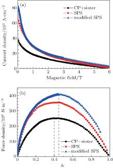
The current carrying properties of the Bi-2212 bulk samples obtained with different fabrication methods were measured with the magnetization method. Because the two SPS samples exhibit higher densities and better texture structures, which lead to larger effective cross section areas, the critical current densities Jc of both SPS and modified SPS samples at zero field increase greatly, as shown in Fig. 5. With the increase of the magnetic field, the modified SPS sample shows the highest Jc over the entire measured magnetic field range, which could be attributed to the enhancement of the flux pinning properties.
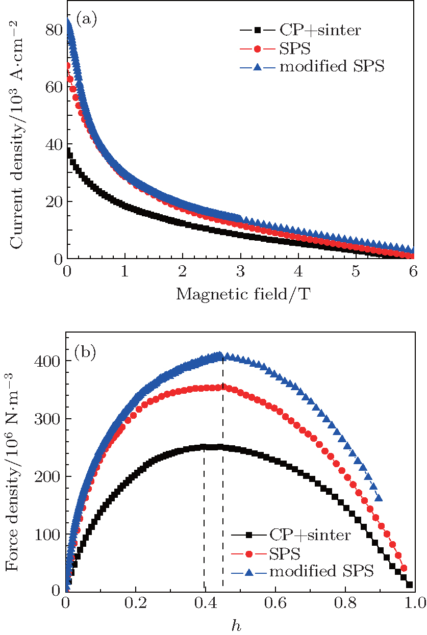 | Fig. 5. (a) Critical current density of Bi-2212 bulks measured at 4.2 K in the magnetic field range from 0 to 6 T. (b) Flux pinning force density as a function of reduced magnetic field h = H/Hirr. |
The flux pinning force density of these bulk samples is calculated as Fp = Jc × B. The obtained flux pinning force density is plotted as a function of the reduced magnetic field h = H/Hirr, where Hirr is the irreversible magnetic field. The Hirr value is determined by the extrapolation method to be 6.0 T, 6.1 T, and 6.7 T for CP + sintering, SPS, and modified SPS samples, respectively. As shown in Fig. 5(b), the peak values of Fp are obtained at the h values of 0.39 for the CP + sintering sample and 0.45 for the two SPS bulk samples, which all represent a mixed flux pinning mechanism with point pinning of normal phase (h = 0.33) and point pinning of Δ κ type (h = 0.50).[40, 41] The shift of the peak value from h = 0.39 to 0.45 represents an increase of the Δ κ type pinning component in the two SPS bulk samples. The pinning centers of Δ κ type are supposed to be superconducting and exhibit different GL parameters with the matrix. Therefore, the well crystallized grain boundaries in the SPS samples with small variation of chemical compositions should be considered as a series of point pinning centers for Δ κ type pinning. The enhancement of the flux pinning force for the modified SPS sample can be attributed to both the enhancement of the intra-granular pinning force density for Abrikosov vortices based on the discussion of the AC susceptibility and the formation of better connected grain boundaries with a large number of defects as the effective flux pinning centers for Δ κ type pinning.
Aiming at the Bi-2212 bulk samples with high densities, better texture structures, and optimized superconducting properties, we developed a modified SPS process. The influences of the modified SPS process, as well as the SPS process on the intergrain connections, flux pinning force, and critical current density have been systematically analyzed. The modified SPS process can not only avoid the amorphous phase at the grain boundaries, but also introduce more flux pinning centers both in the grains and at the grain boundaries, which lead to the obvious enhancement of current carrying properties.
The authors appreciate the discussion with Dr. J. G. Noudem from CNRS.
| 1 |
|
| 2 |
|
| 3 |
|
| 4 |
|
| 5 |
|
| 6 |
|
| 7 |
|
| 8 |
|
| 9 |
|
| 10 |
|
| 11 |
|
| 12 |
|
| 13 |
|
| 14 |
|
| 15 |
|
| 16 |
|
| 17 |
|
| 18 |
|
| 19 |
|
| 20 |
|
| 21 |
|
| 22 |
|
| 23 |
|
| 24 |
|
| 25 |
|
| 26 |
|
| 27 |
|
| 28 |
|
| 29 |
|
| 30 |
|
| 31 |
|
| 32 |
|
| 33 |
|
| 34 |
|
| 35 |
|
| 36 |
|
| 37 |
|
| 38 |
|
| 39 |
|
| 40 |
|
| 41 |
|