Wei Jiang-Bin, Chi Xiao-Wei, Lu Chao, Wang Chen, Lin Guang-Yang, Wu Huan-Da, Huang Wei†, Li Cheng‡, Chen Song-Yan, Liu Chun-Li. Modulation of WN x/Ge Schottky barrier height by varying N composition of tungsten nitride . Chinese Physics B, 24(7): 077306
Permissions
Modulation of WN x/Ge Schottky barrier height by varying N composition of tungsten nitride
Wei Jiang-Bina), Chi Xiao-Weia), Lu Chaoa), Wang Chena), Lin Guang-Yanga), Wu Huan-Daa), Huang Wei†a), Li Cheng‡a), Chen Song-Yana), Liu Chun-Lib)
Department of Physics, Semiconductor Photonics Research Center, Xiamen University, Xiamen 361005, China
Department of Physics, Hankuk University of Foreign Studies, Yongin 449-791, Korea
*Project supported by the National Natural Science Foundation of China (Grant Nos. 61176092 and 61474094), the National Basic Research Program of China (Grant Nos. 2012CB933503 and 2012CB632103), and the National Natural Science Foundation of China–National Research Foundation of Korea Joint Research Project (Grant No. 11311140251).
Abstract
Modulation of the Schottky barrier heights was successfully demonstrated for WN x/p-Ge and WN x/n-Ge contacts by increasing the nitrogen component in the WN x films. The WN0.38/p-Ge contact exhibits rectifying characteristic and an apparent Schottky barrier of 0.49 eV while the WN0.38/n-Ge Schottky contact exhibits quasi-Ohmic current–voltage characteristics. Dipoles formed at the contact interface by the difference of the Pauling electronegativities of Ge and N are confirmed to alleviate the Fermi-level pinning effect.
Germanium (Ge) is considered to be a good candidate material due to its high carrier mobilities and large optical absorption coefficient at the wavelength for optical communication in electronic and photonic device applications. Although a high performance p-type Ge channel metal– oxide– semiconductor field-effect transistor (MOSFET) has been demonstrated, [1] the n-type Ge channel MOSFET still suffers from two serious challenges: (a) low electrical activation of donor impurities and fast diffusion of n-Ge dopant that hinder fabricating low resistivity, shallow source/drain junctions.[2] (b) strong Fermi-level pinning effect on Ge in the vicinity of the valence band maximum of Ge results in a high effective electron Schottky barrier height (SBH) when metals contact with n-Ge. The high SBH results in high series contact resistivity[3] while Ohmic contact with p-Ge is normally achieved.
To control the SBHs of the metal/Ge contact, several methods have been proposed to alleviate the FLP effect. One is inserting an ultrathin insulating interfacial layer (e.g., TiO2, [4] Al2O3, [5] GeOx, [6] Si3N4, [7] a-Ge[8]). Segregation of addictive elements (such as S, [9] Se, [10] P, [11]) at the metal/Ge interface is another. Recently, metallic nitrides such as TiN[12] and TaN[13] have been confirmed to form Ohmic contact to n-type Ge intrinsically. In this work we study the SBHs of the WNx film on both n-type and p-type Ge (100) substrates with various N compositions. Typical electrical rectifying characteristics of the WNx/p-Ge contact and Ohmic contact of WNx/n-Ge are obtained.
2. Experimental procedure
P-type and n-type Ge (100) substrates with a resistivity of 0.1 Ω · cm were used for schottky diodes fabrication. All of the Ge wafers were firstly circularly degreased in an ultrasonic bath of acetone and ethanol, and then immersed in hydrofluoric acid solution (HF:H2O = 1:50) to remove the native oxide, rinsed with deionized water, and finally blown dry by nitrogen. The diode areas were defined by conventional lithography. Then WNx thin films were deposited on these substrates by reactive sputtering in a magnetron sputtering system (JC-500-3/D D.C.) with mixed N2– Ar gas atmosphere for 30 min. The base vacuum pressure of the sputtering system was 1.0 × 10− 3 Pa. Tungsten with a purity of 99.99% was used as the target. During sputtering, the Ar gas flow was fixed at 50 sccm while the N2 gas flow was changed from 0 sccm to 35 sccm. For the electrical measurement, WNx/Ge contacts with a diameter of 120 μ m were formed by a lift-off process and a 300-nm Al layer was sputtered on the backside of the wafers to form the Ohmic contact. The samples were analyzed by four point probes, x-ray diffraction (XRD), x-ray photoelectron spectroscopy (XPS), and I– V characteristics.
3. Results and discussion
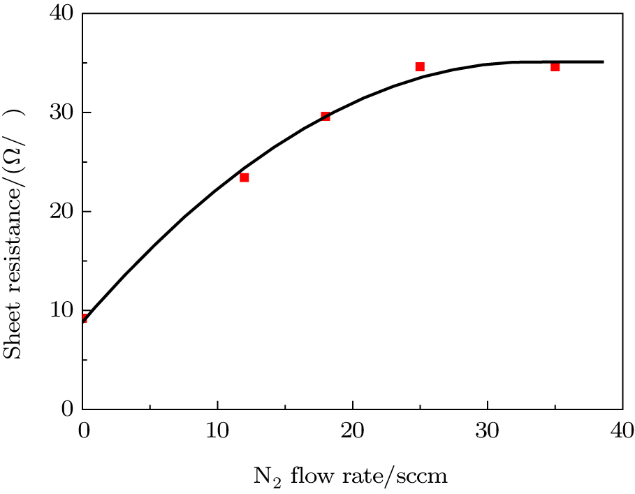
Because the growth rates under different N2 flow rates are all about 4 nm/min, the thicknesses of the obtained WNx films with different N2 flow rates are all around 120 nm. Sheet resistances of the WNx films with different N2 flow rates are shown in Fig. 1. For pure W film, the resistivity is calculated to be about 120 μ Ω · cm, which is higher than the resistivity data for bulk W (∼ 5.5 μ Ω · cm) because of surface/grain boundary scattering. When the N2 flow rates increase, sheet resistance of the WNx film become even higher than that of pure W. However, when the N2 flow rate is above 25 sccm, the sheet resistance of WNx tends to be stable at about 34 Ω /◻ . The increase of the film resistivity was ascribed to the increasing inclusion of nitrogen atoms in the WNx crystal lattice which can bring appreciable band structure changes and a decreasing carrier density.
Fig. 1. Sheet resistance of the WNx film fabricated with various rates of N2 flow from 0 sccm to 35 sccm.
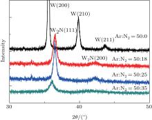
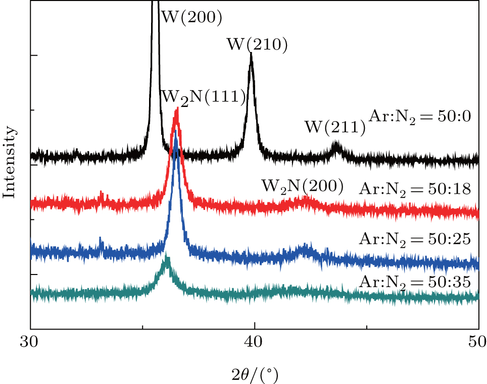
XRD is used to identify the crystalline phases of the samples. Figure 2 shows the XRD patterns of the WNx films with different N compositions. The W(200), W(210), and W(211) diffraction peaks are clearly observed for the W deposited in pure Ar atmosphere. When the N2 flow reaches 18 sccm, the crystalline phase is identified as W2N and all the films show a preferred orientation of (111). However, the peak positions are a little lower than the standard value of 37.73° for W2N(111) in the ICDD cards.[14] A continuous left shift of the W2N(111) x-ray diffraction peak with further increasing of the N2 flow, is found to be consistent with the gernerally reported data. This has been explained by the existence of nitrogen excess in the interstitial positions of the W2N lattice and the expansion of the W2N lattice.[15]
Fig. 2.θ – 2θ XRD scan of the WNx film formed at different N2 flow rates from 0 to 35 sccm.
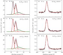
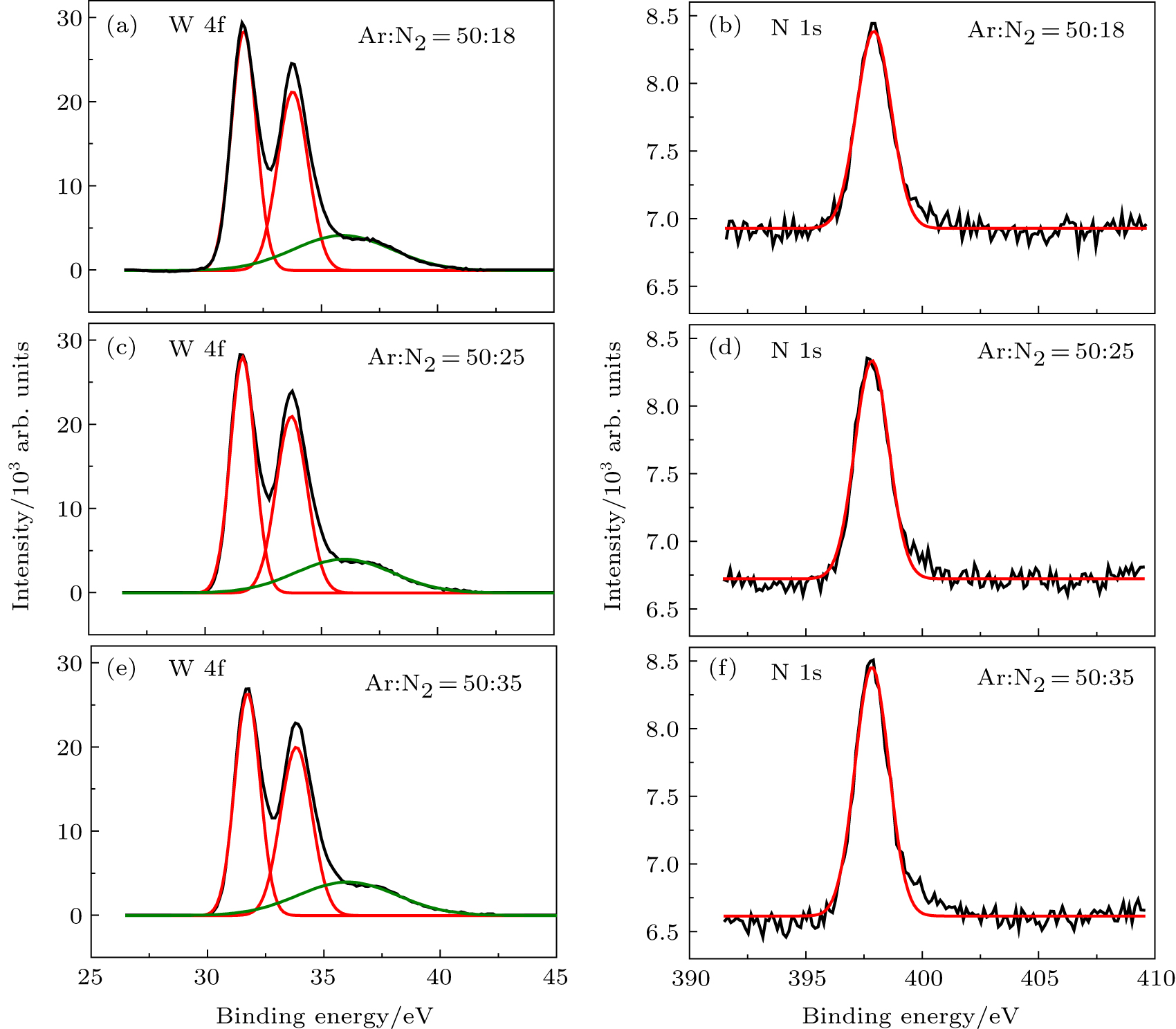
In order to evaluate the nitrogen component of the WNx films, the deconvoluted W 4f XPS spectrum is depicted in Fig. 3. The W 4f spectrum pertained to W– N and W– O bonds and there is no obvious W– W bonds. The W– O bond was caused by residual oxygen in the deposition chamber. The simulated W 4f 7/2– W 4f 5/2 peaks located at 31.6 eV and 33.7 eV shall pertain to the W2N phase (W– N bond).[16] In addition, the 397.5– 397.6 eV binding energy of N 1s electrons was close to the reported value for W2N (397.3 eV). By integrating the XPS peaks’ area, the nitrogen component x of these samples was determined to be x = 0.28, 0.32, and 0.37. Both XRD and XPS measurements indicate that the nitrogen components increase as the N2 flow rate increases.
Fig. 3. XPS spectra of W 4f and N 1s for the WNx films prepared with different Ar/N2 flow rates. (a) W 4f, Ar : N2 = 50 : 18, (b) N 1s, Ar : N2 = 50 : 18, (c) W 4f, Ar : N2 = 50 : 25, (d) N 1s, Ar : N2 = 50 : 25, (e) W 4f, Ar : N2 = 50 : 35, (f) N 1s, Ar : N2 = 50 : 35.
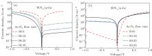
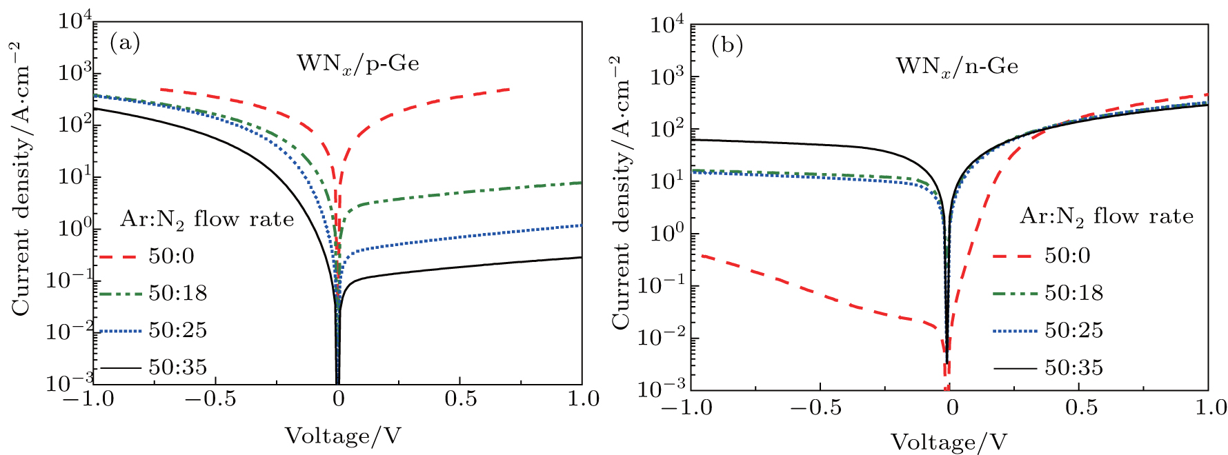
Figure 4 shows the current density– voltage (J– V) characteristics measured at room temperature for WNx/p-Ge and WNx/n-Ge contacts prepared under two different compositions of W nitride. The J– V curve of the W/Ge contact is also shown for comparison. The thermionic emission model is used to extract the SBH of the samples with rectification characteristics. The relationship between current (I) and voltage (V) used for the calculations is expressed as
where Is is the reverse saturation current, A* is the Richardson constant (A* = 143 A· cm− 2· K− 2 for n-Ge and A* = 43 A· cm− 2· K− 2 for p-Ge), kB is the Boltzman constant, A = 2.01 × 10− 4 cm− 2 is the diode area, Φ B is the SBH, n is the ideality factor, q is the electron’ s charge, V is the applied bias, and Rs is the series resistance. The SBHs extracted from the J– V curves of the WNx/Ge contact are shown in Table 1.
Fig. 4.J– V characteristics of the WNx/Ge films formed with different Ar/N2 flow rate ratios. (a) WNx/p-Ge (b) WNx/n-Ge.
Table 1.
Table 1.
Table 1. The extracted SBHs of different samples and their rectification ratios under ± 1.0 V bias. “ (O)” denotes Ohmic or quasi-Ohmic contact.
Type of Ge
N2 flow rate/sccm
Rectification ratio @ – 1 V/1 V
Ideality factor
SBH/eV
n-type
0
1159
1.28
0.50
18
31
1.15
0.37
25
33
1.37
0.37
35
13
–
(O)
p-type
0
1
–
(O)
18
49
1.72
0.37
25
314
1.81
0.42
35
765
1.76
0.49
Table 1. The extracted SBHs of different samples and their rectification ratios under ± 1.0 V bias. “ (O)” denotes Ohmic or quasi-Ohmic contact.
Typical rectifying characteristics are observed for the Schottky W/n-Ge contact. With the increase of the N composition in the W nitride, the reverse saturation current density of WNx/n-Ge increases while the forward current density of WNx/p-Ge decreases. The electrical property of WNx/n-Ge gradually changes from rectification of 0.50 eV to Ohmic while that of WNx/p-Ge changes from Ohmic to rectification of 0.49 eV. A rectification ratio of nearly 103 for WNx/p-Ge is obtained as the N2 flow rate reaches 35 sccm. As is well known, Ohmic characteristics for p-Ge were experimentally observed irrespective of the metal vacuum work-function because the Fermi-levels at metal/Ge interfaces are pinned near the valence band edge of Ge. However, the significant SBH modulation of WNx/p-Ge is observed in the experiment, illustrating that some mechanisms act on the WNx/p-Ge contact and realize the Femi level depinning effect.
There are several mechanisms to explain the SBH modulation of the metal-semiconductor contact. One widely recognized mechanism is to minimize metal-induced gap states (MIGS)[17, 18] by inserting an interfacial insulating layer which blocks the electron wave function penetrating from the metal into the semiconductor. Other authors have argued that the interface defects caused by ion implantation or dipoles at the metal-semiconductor interface at the metal-semiconductor interface will also alter the effective SBH. In the case of WNx/Ge contact, MIGS is obviously not applicable to explain the SBH modulation effect because the metallic WNx film does not block penetrating the electron wave. If we consider the interface defect mechanism, the obtained low effective SBH is formed by the current leakage through the interface defects. Such a leakage is natural regardless on the conduction type of the contact semiconductor, and the low rectification ratios or Ohmic behavior should be observed on both metal/n-Ge and metal/p-Ge contacts. However, in our WNx/p-Ge contact sample, the rectifying characteristics are clearly observed. This result explicitly excluded the possibility of interface leakage by defects, but further illustrated the validity of the dipoles layer model which was recently reported by Wu et al.[19] One may further argue that the different work functions of WNx could be the reason of SBH changing. According to the previous report written by Jiang (Ref. [16]), the work functions range from 4.39 eV to 5.01 eV for WNx with various N contents compared to 4.67 eV for pure W. However, those work functions are not monotonous as the N content increases. It is also difficult to conclude any correlation between the work function of WNx and the SBH evolution even if the surface Fermi-level pinning effect is ignored.
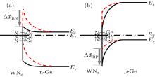
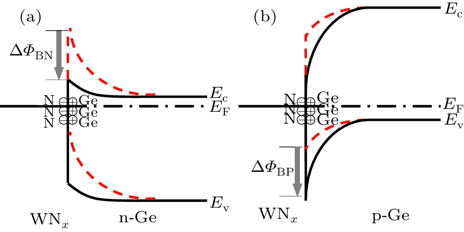
According to the dipoles layer model, the N and W atoms formed bonds with Ge at the WNx/Ge contact interface. However, the N– Ge bond is not pure covalent but partially ionic because the Pauling electronegativities of Ge (2.01) and N (3.04) are largely discrepant, so many N– Ge bonds can be dealt with as interfacial dipoles (see Fig. 5). The potential drop arose from the interfacial dipoles strongly affecting the energy band bending and modulating the WNx/Ge contact SBH. From our experiment results shown in Table 1, it is clearly observed that the SBH modulation tendency of the WNx/p-Ge is just contrary to that of the WNx/n-Ge, just providing a direct evidence of the dipoles layer model which was established for WNx/Ge contact.
Fig. 5. Schematic band diagram of the pinning-alleviated WNx/n-Ge (a) and WNx/p-Ge (b) contacts by the interfacial dipoles layer. Here, Ec is the conduction band edge, Ev is the valence band edge, and EF is the Fermi level.
4. Conclusions
In summary, thin WNx films have been fabricated by reactive magnetron sputtering of tungsten in an Ar– N2 gas mixture of different flow rates. As the N2 flow rates increase, the nitrogen components increase from 0 to 0.38. By increasing the nitrogen components of the WNx film, the contact properties have been drastically changed from Schottky to Ohmic for n-Ge and from Ohmic to Schottky characteristics for p-Ge, respectively. The SBH of WNx/n-Ge gradually changes from 0.50 eV to a value smaller than 0.30 eV while the SBH of WNx/p-Ge changes from a value smaller than 0.30 eV to 0.49 eV. This experimental fact strongly suggests that the dipoles layer model is the dominant SBH mechanism in the WNx/Ge contact.
... semiconductor field-effect transistor (MOSFET) has been demonstrated,[1] the n-type Ge channel MOSFET still suffers from two serious challenges: (a) low electrical activation of donor impurities and fast diffusion of n-Ge dopant that hinder fabricating low resistivity, shallow source/drain junctions ...
1
2008
0.0
0.0
... [2] (b) strong Fermi-level pinning effect on Ge in the vicinity of the valence band maximum of Ge results in a high effective electron Schottky barrier height (SBH) when metals contact with n-Ge ...
1
2006
0.0
0.0
... The high SBH results in high series contact resistivity[3] while Ohmic contact with p-Ge is normally achieved ...
... Segregation of addictive elements (such as S,[9] Se,[10] P,[11]) at the metal/Ge interface is another ...
1
2012
0.0
0.0
... Segregation of addictive elements (such as S,[9] Se,[10] P,[11]) at the metal/Ge interface is another ...
1
2011
0.0
0.0
... Segregation of addictive elements (such as S,[9] Se,[10] P,[11]) at the metal/Ge interface is another ...
1
2013
0.0
0.0
... Recently, metallic nitrides such as TiN[12] and TaN[13] have been confirmed to form Ohmic contact to n-type Ge intrinsically ...
1
2012
0.0
0.0
... Recently, metallic nitrides such as TiN[12] and TaN[13] have been confirmed to form Ohmic contact to n-type Ge intrinsically ...
1
0.0
0.0
... [14] A continuous left shift of the W2N(111) x-ray diffraction peak with further increasing of the N2 flow, is found to be consistent with the gernerally reported data ...
1
2012
0.0
0.0
... [15] ...
2
2006
0.0
0.0
... [16] In addition, the 397 ...
... [16]), the work functions range from 4 ...
1
2007
0.0
0.0
... One widely recognized mechanism is to minimize metal-induced gap states (MIGS)[17,18] by inserting an interfacial insulating layer which blocks the electron wave function penetrating from the metal into the semiconductor ...
1
2010
0.0
0.0
... One widely recognized mechanism is to minimize metal-induced gap states (MIGS)[17,18] by inserting an interfacial insulating layer which blocks the electron wave function penetrating from the metal into the semiconductor ...
1
2014
0.0
0.0
... [19] One may further argue that the different work functions of WNx could be the reason of SBH changing ...
Modulation of WN x/Ge Schottky barrier height by varying N composition of tungsten nitride
[Wei Jiang-Bina), Chi Xiao-Weia), Lu Chaoa), Wang Chena), Lin Guang-Yanga), Wu Huan-Daa), Huang Wei†a), Li Cheng‡a), Chen Song-Yana), Liu Chun-Lib)]


 , Li Cheng‡