


A novel physical parameter extraction approach for Schottky diodes
[Wang Hao, Chen Xing† , Xu Guang-Hui, Huang Ka-Ma]
, Xu Guang-Hui, Huang Ka-Ma]
|
|


†Corresponding author. E-mail: xingc@live.cn
*Project supported by the Joint Fund of the National Natural Science Foundation of China and the China Academy of Engineering Physics (Grant No. U1230112).
Parameter extraction is an important step for circuit simulation methods that are based on physical models of semiconductor devices. A novel physical parameter extraction approach for Schottky diodes is proposed in this paper. By employing a set of analytical formulas, this approach extracts all of the necessary physical parameters of the diode chip in a unique way. It then extracts the package parasitic parameters with a curve-fitting method. To validate the proposed approach, a model HSMS-282c commercial Schottky diode is taken as an example. Its physical parameters are extracted and used to simulate the diode’s electrical characteristics. The simulated results based on the extracted parameters are compared with the measurements and a good agreement is obtained, which verifies the feasibility and accuracy of the proposed approach.
The physical-model-based simulation[1– 6] possesses some advantages when compared to the widely used equivalent-model-based simulation; for example, it is naturally able to accurately simulate semiconductor devices and circuits under various conditions, especially at high frequencies or with a large signal input, and it reveals useful physical mechanisms. In our previous work, [5, 6] a novel physical-model-based simulation approach was proposed. Although the physical parameters of the semiconductor devices are needed for the physical-model-based simulation, they are not usually provided by the manufacturers. Hence, parameter extraction for the physical model of semiconductor devices is a primary and important task.
Currently, most research regarding the parameter extraction of semiconductor devices concerns the equivalent-circuit models. Few studies focus on the parameter extraction for the physical models of semiconductor devices. One widely used method to extract the physical parameters is the curve-fitting method, which obtains the parameters by fitting the simulated data to the measured data.[5, 7] However, this method is usually time-consuming. Moreover, it has a defect, as noted in Ref. [8], in that erroneous results may be obtained if too many dependent physical parameters are determined simultaneously. In other words, the parameters extracted by the curve fitting method may not be unique.
Another effective extraction method is the analytical method, which utilizes formulas that describe the relationship between the device’ s physical parameters and its electric characteristics to perform the extraction. For example, a formula to extract the doping profile of metal– oxide– semiconductor (MOS) devices from their capacitance– voltage (C– V) characteristics was derived in Ref. [9]. Some formulas derived from the current– voltage relationship of Schottky diodes have been exploited to calculate their saturation current and barrier height.[10, 11] However, nearly all of the previous work employed analytical formulas for extracting only one or several physical parameters of the corresponding devices. Moreover, they seldom considered the parasitic parameters of the semiconductor device packages.[10– 14] In fact, the parasitic parameters of the package may significantly affect a device’ s performance, especially at high frequencies. Importantly, the extracted parameters of a semiconductor device may be inaccurate if the packages’ parasitic parameters are neglected. The degree of this inaccuracy will be estimated later. Hence, for the physical-model-based simulation, a parameter extraction method that can effectively and uniquely extract all the necessary physical parameters, including both the device chip parameters and the package parasitic parameters, is quite desirable.
In this paper, we present a straightforward step-by-step parameter extraction procedure for Schottky diodes. It uses a set of analytical formulas to uniquely extract the diode chip physical parameters, and then extracts the package parasitic parameters using a curve-fitting method. The remainder of this paper is organized as follows. The physical model and parameters of the Schottky diode are introduced in Section 2, and the proposed approach is presented in Section 3. Then, in Section 4, a model HSMS-282c commercial Schottky diode is taken as an example to validate the proposed approach. Finally, the conclusions are drawn in Section 5.
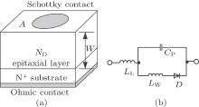
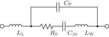
As illustrated in Fig. 1(a), a Schottky diode chip mainly consists of two regions: the first is the epitaxial layer with doping concentration ND and thickness W; and the second is the highly doped substrate, which can be treated as a resistor with a low resistance. On top of the epitaxial layer there is a Schottky contact with barrier height Φ B and metal work function Φ M. The effective area of the diode is denoted by A. As shown in Fig. 1(b), the package parasitics of the Schottky diode can be modeled by an equivalent circuit in which the Schottky diode chip D is connected to three lumped elements, where LL is the lead inductance, LW is the bond wire inductance, and CP is the package capacitance.[15]
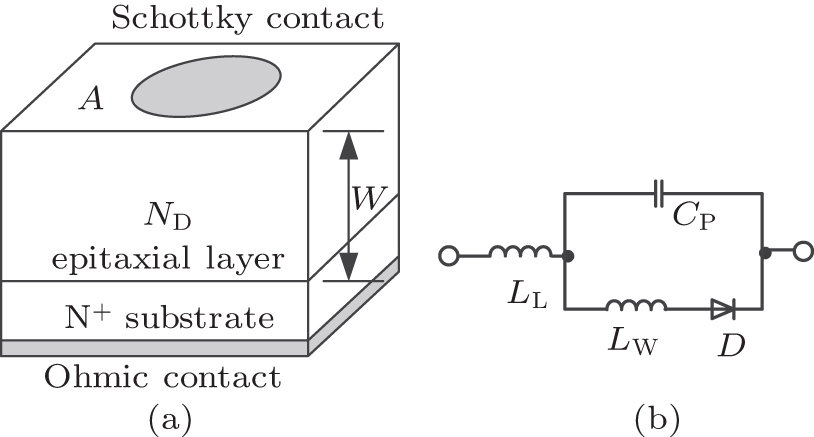 | Fig. 1. The physical parameters of a Schottky diode: (a) diode chip physical parameters, and (b) package parasitic parameters. |
The proposed approach includes the following six steps to extract the Schottky diode’ s physical parameters. For clarification, this section takes the silicon Schottky diode HSMS-282c as an example. It is worth noting that the parameter extraction procedure is suitable for all types of semiconductor materials.
The current– voltage relation of a Schottky diode is given by[16]
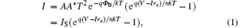
where IS is the saturation current, A is the diode area, A* is Richardson’ s constant, T is the temperature, q is the electron charge, Φ B is the barrier height, k is Boltzmann’ s constant, V is the applied voltage across the Schottky diode, rs is the series resistance, and n is the ideality factor.
The threshold voltage of a diode is the minimum forward voltage across the terminals of the diode at which the diode starts to conduct a current. Let Vth denote the threshold voltage of a Schottky diode. When V < Vth, the series resistance rs can be neglected due to the high resistivity of the Schottky barrier, thus equation (1) can be expressed as

A detailed theoretical derivation for Eq. (2) is given in Ref. [17]. After measuring the I– V characteristic of a Schottky diode, the plot of log[I/(1 − e− qV/kT)] versus V can be drawn. This plot is linear, as shown in Fig. 2, for the HSMS-282c Schottky diode. As illustrated in the figure, the saturation current IS is determined by extrapolating the linear curve to V = 0, and the ideality factor n is calculated from the slope of the curve by

where m is the slope of the linear curve.
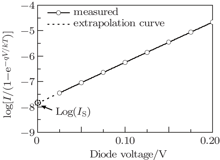 | Fig. 2. Current– voltage characteristic of the HSMS-282c Schottky diode measured at room temperature (300 K). |
For the HSMS-282c Schottky diode, the saturation current IS and ideality factor n are calculated to be 0.139 nA and 1.06, respectively.
If V < Vth and V ≫ kT/q, then equation (1) can be approximated by[17]

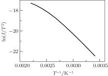
For a constant forward bias voltage V1, the diode current will change with the temperature. Thus, the I– T characteristic of a Schottky diode can be measured at a constant forward bias voltage. Then, a plot of ln(I/T2) versus 1/T, which is commonly called the Richardson plot, can be created. It has a slope of − q(Φ B − V1/n)/k, as indicated in Eq. (4). The barrier height is then given by
For the HSMS-282c Schottky diode, the I– T characteristic (see Fig. 3) is measured at a forward voltage of 0.2 V for the temperature range of 293– 453 K. Here, V1 = 0.2 V is chosen because it is smaller than Vth (approximately 0.3 V) and much larger than kT/q in the temperature range of 293– 453 K. With the ideality factor n obtained in Step 1, the barrier height can be calculated using Eq. (5). The calculated barrier height Φ B is 0.629 V for the HSMS-282c diode.
 | Fig. 3. Richardson plot of the HSMS-282c Schottky diode measured at a forward voltage of 0.2 V for the temperature range of 293– 453 K. |
The metal work function of a Schottky contact can be determined by

where χ is the electron affinity of the semiconductor. For the HSMS-282c silicon Schottky diode, χ is 4.05 V, [16] and thus Φ M is 4.679 V.
From Eq. (1), it is known that

Here, the Richardson’ s constant A* is chosen to be 110 A· K− 2· cm− 2 for the silicon. The contact area A can be obtained from Eq. (7) because all of the other parameters are known. The area A is 6× 10− 5 cm2 for the HSMS-282c Schottky diode.
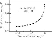
The total capacitance of a reverse-bias Schottky diode is given by[18]
where Ctot is the total capacitance, CJ0 is the zero-bias junction capacitance, Φ BI is the built-in potential, and CP is the parasitic capacitance.
Figure 4 shows the total capacitance, which is obtained from the C– V measurement, [19] for the HSMS-282c Schottky diode. The three parameters, CJ0, Φ BI, and CP, can be determined from Eq. (8) with three different sets of Ctot– V values. The extracted values are CJ0 = 0.65 pF, Φ BI = 0.56 V, and CP = 0.16 pF.
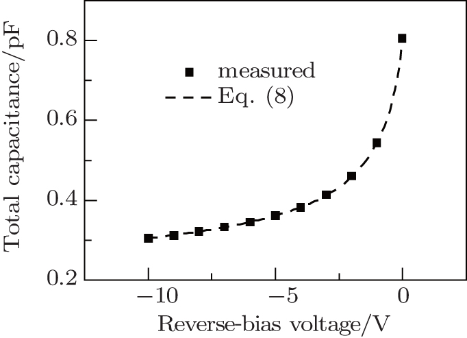 | Fig. 4. Total capacitance of the HSMS-282c Schottky diode versus the reverse-bias voltage. |
The zero-bias junction capacitance is given by[17, 20]

and

where ε is the dielectric constant of the semiconductor, ND is the doping concentration of the epitaxial layer, and W is the thickness of the epitaxial layer. The doping concentration and the thickness of the epitaxial layer are, therefore, obtained by solving Eqs. (9) and (10), respectively. For the HSMS-282c device, ε r is 11.7, thus, the extracted parameters are ND = 7.9 × 1014 cm− 3 and W = 0.96 μ m.
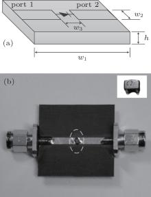
Until now, all of the physical parameters listed in Section 2 have been obtained, except for the parasitic inductances LL and LW. In this step, these two parameters are extracted from the S parameters of a two-port microstrip circuit, which is illustrated in Fig. 5. Figure 5(a) is a schematic diagram of the circuit, and figure 5(b) is a fabricated circuit. By fitting the simulated parameters | S11| and | S21| of this circuit to the measured data, the parasitic inductances are obtained.
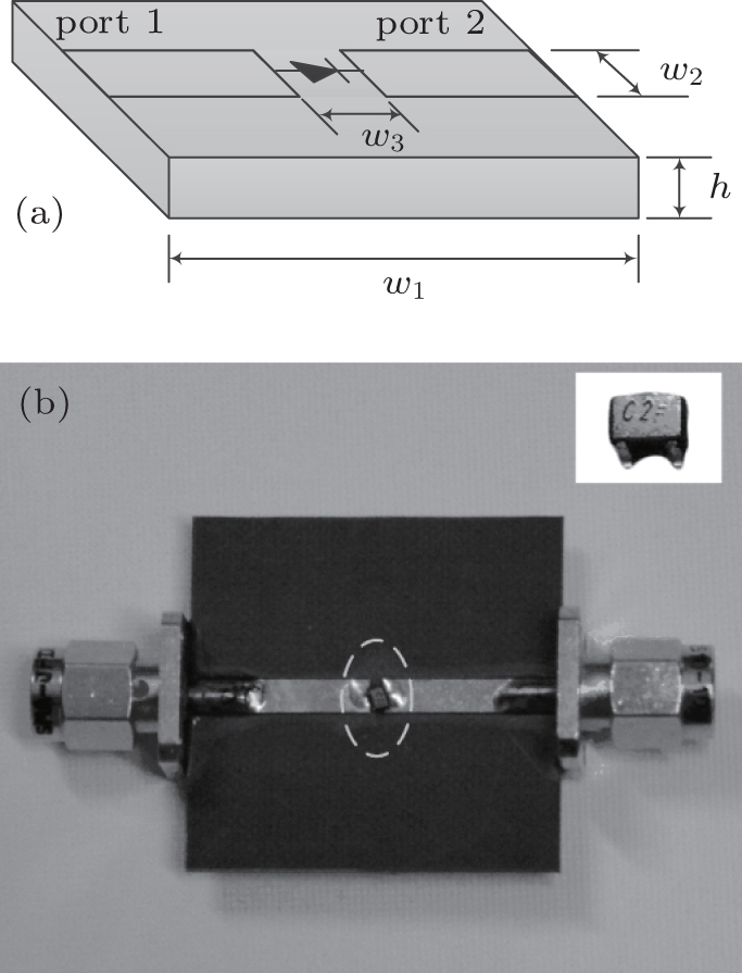 | Fig. 5. (a) Schematic diagram of a two-port microstrip circuit. (b) Photo of the fabricated circuit for extracting the parasitic inductances of the HSMS-282c Schottky diode. (Physical dimensions: w1 = 31.1 mm, w2 = 2.75 mm, w3 = 1.1 mm, and h = 1 mm. Relative permittivity of substrate: ε r = 2.55). |
To simplify the calculation and reduce the calculation time, the simulation of the S parameters is performed using a small signal model instead of the physical model of the Schottky diode. The small signal model (see Fig. 6) is a linear equivalent circuit model, which is used to describe the diode’ s linear electrical behavior in the S-parameter simulation.
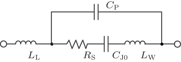 | Fig. 6. Small signal model of a Schottky diode. |
In this small signal model, the zero-bias junction capacitance CJ0 and the package capacitance CP are those obtained in Step 4, the series resistance RS can be extracted using the power exponent method, and then the parasitic inductances LL and LW are extracted from the two-port S-parameter data using a curve-fitting method.
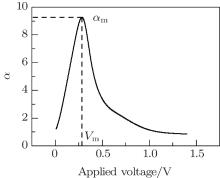
The power exponent parameter α is defined as[21]

The series resistance RS is calculated by

where α m is the maximum value of α ; and Vm and Im are the corresponding bias voltage and current. The α – V characteristic of the HSMS-282c diode is shown in Fig. 7, and the calculated series resistance is 7.85 Ω .
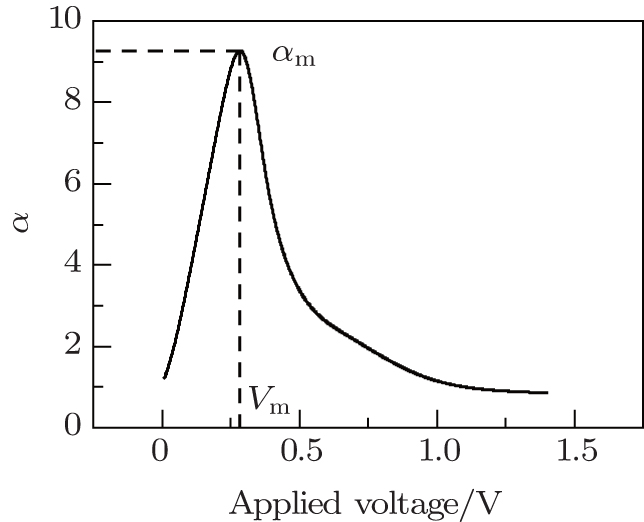 | Fig. 7. Power exponent of the HSMS-282c Schottky diode versus the applied voltage. |
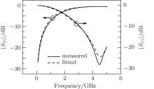
Figure 8 shows the measured and fitted S parameters for the HSMS-282c diode. The extraction results are as follows: the lead inductance LL is 0.79 nH, and the bond wire inductance LW is 1.07 nH.
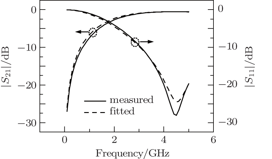 | Fig. 8. Measured and fitted S parameters of the fabricated microstrip circuit. |
All of the physical parameters have been extracted thoroughly, including both the diode chip physical parameters and the package parasitic parameters. Table 1 lists the extracted physical parameters, of the HSMS-282c Schottky diode, which are necessary for the physical-model-based simulation. As can be seen, the package capacitance is approximately 0.16 pF, which is as much as 20% of the total capacitance (see Fig. 4) at zero bias. If the package capacitance is neglected and the total capacitance is mistakenly regarded as the junction capacitance in the parameter extraction then, as in some previous work, [22] significant errors may be introduced into the extraction results.
| Table 1. Extracted physical parameters. |
To validate the proposed extraction approach for Schottky diodes, the extracted results of the HSMS-282c diode are used to simulate the direct-current (dc), alternating-current (ac), and high frequency characteristics of this diode using the physical-model-based simulation approach that we have previously proposed, [5, 6] and the simulation results are compared with the measured data.
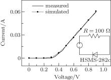
The inset of Fig. 9 shows a dc circuit that is comprised of a dc source, a 100 Ω resistance, and an HSMS-282c diode. As illustrated in Fig. 9, the agreement between the simulated (dotted line) I– V characteristic based on the extracted parameters and the measured (solid line) static characteristic is quite satisfying.
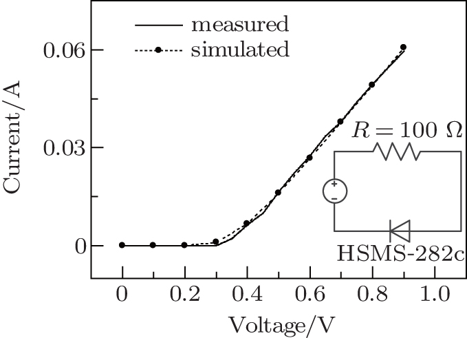 | Fig. 9. Comparison of the simulated and measured static characteristics of an HSMS-282c Schottky diode. The inset shows the dc circuit. |
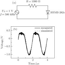
Figure 10(a) shows a low frequency circuit consisting of an HSMS-282c diode, an ac source with voltage amplitude US = 1 V, and a resistor R = 1 kΩ . Its ac characteristic at frequency f = 500 kHz is simulated, and the result is compared with the measurement using a Tektronix TDS1012 oscilloscope. Figure 10(b) shows the comparison of the simulated (dashed line) and measured (solid line) voltages across the HSMS-282c diode. As illustrated in the figure, the simulated result agrees well with the measured result, except that the measured result contains some noise.
 | Fig. 10. (a) Circuit for the ac characteristics. (b) Comparison of the simulated and measured terminal voltages of an HSMS-282c Schottky diode. |
The high frequency characteristics of a two-port microstrip circuit (see Fig. 5) are also analyzed. The transmitted and reflected voltages of this microstrip circuit are simulated for a source signal with a frequency of 2.45 GHz and a power of 20 dBm incident on port 1 and they are then compared with the measured data, which are obtained by an Agilent high performance oscilloscope DSA91204A. Figures 11(a) and 11(b) show that the simulated and measured results agree very well, and both indicate that the voltage waveforms are no longer sine waves. This characteristic is due to the dc and harmonic components of the transmitted and reflected voltage waves caused by the nonlinear characteristic of the Schottky diode. Figure 12 gives the simulated spectrum from a Fourier transform and the corresponding measured spectrum for the reflected and transmitted voltage waves. A good agreement can be observed between the simulated and the measured data.
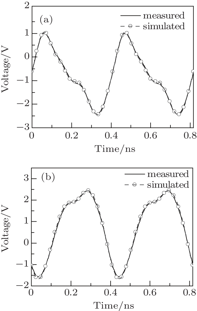 | Fig. 11. Port voltages of the two port microstrip circuit: (a) reflected wave on port 1, (b) transmitted wave on port 2. |
 | Fig. 12. (a) Spectrum of the reflected wave on port 1. (b) Spectrum of the transmitted wave on port 2. |
In this study, a novel extraction approach for obtaining the physical parameters of Schottky diodes is presented. This approach extracts the parameters in a step-by-step manner using a set of analytical formulas together with a curve fitting method.
As an example, the physical parameters of a model HSMS-282c Schottky diode are extracted. Then, the extracted parameters are utilized in the physical-model-based simulation to obtain the electrical characteristics of circuits containing the Schottky diode, including the dc, ac, and high frequency characteristics. The simulation results are highly consistent with the experimental results, which demonstrates the accuracy of the extracted results.
With a further increase in computing power, the physical-model-based simulation will be increasingly attractive to circuit engineers. In the future, more extraction procedures should be proposed for different types of semiconductor devices to obtain their physical parameters.
| 1 |
|
| 2 |
|
| 3 |
|
| 4 |
|
| 5 |
|
| 6 |
|
| 7 |
|
| 8 |
|
| 9 |
|
| 10 |
|
| 11 |
|
| 12 |
|
| 13 |
|
| 14 |
|
| 15 |
|
| 16 |
|
| 17 |
|
| 18 |
|
| 19 |
|
| 20 |
|
| 21 |
|
| 22 |
|