Energy distribution extraction of negative charges responsible for positive bias temperature instability
Ren Shang-Qing†

, Yang Hong, Wang Wen-Wu‡
, Tang Bo, Tang Zhao-Yun, Wang Xiao-Lei, Xu Hao, Luo Wei-Chun, Zhao Chao, Yan Jiang, Chen Da-Peng, Ye Tian-Chun
Institute of Microelectronics of Chinese Academy of Sciences, Key Laboratory of Microelectronics Devices and Integrated Technology, Beijing 100029, China
†Corresponding author. E-mail: renshangqing@ime.ac.cn
‡Corresponding author. E-mail: wangwenwu@ime.ac.cn
*Project supported by the National Science & Technology Major Projects of the Ministry of Science and Technology of China (Grant No. 2009ZX02035) and the National Natural Science Foundation of China (Grant Nos. 61176091 and 61306129).
1. IntroductionWith the feature size of CMOSFET scaling down, the high-k/metal gate has replaced the conventional silicon dioxide/poly-silicon gate since 45 nm technology node.[1, 2] Although the device performance has been promoted significantly, such as drain current enhancement and gate leakage reduction, reliability issues of high-k/metal gate devices are becoming more serious and complicated due to introducing a dual-layer structure of the dielectric compared with the traditional monolayer silicon dioxide.[3– 5] Positive bias temperature instability (PBTI), one of the most important concerns, has become more serious and attracts much attention. Three theories have been proposed to explain the PBTI characteristics. The most acceptable one is that electrons are trapped by pre-existing traps when tunneling through the interface layer (IL) into the high-k bulk.[6– 9] The second one is that stress induced defects transfer into traps and trap tunneling electrons.[10, 11] The combination of the creation of an interface state with electron trapping is also proposed regarding the ultrathin gate dielectric.[12, 13] In the present work, unlike other work, the microscopic properties of the negative trapped charges and traps are investigated during PBTI stress instead of the degradation mechanism, based on the recovery measurement, including the energy distribution of the negative trapped charges under different PBTI stresses.
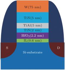
2. ExperimentThe devices tested were fabricated by a standard high-k/metal gate last process. The gate dielectric comprises an interface layer of 0.6 nm silicon dioxide and 2.2 nm hafnium dioxide, chemically grown by ozone and atomic layer deposition (ALD), respectively. Post-deposition annealing (PDA) followed the gate dielectric fabrication in nitrogen atmosphere at 450 ° C. The metal gate stacks comprise of 2.0 nm TiN, 5.0 nm TiAl, 5.0 nm TiN, and 75 nm W, which were fabricated by ALD, physical vapor deposition (PVD), PVD, and ALD, respectively. The effective oxide thickness (EOT) is 0.9 nm finally extracted from the C– V curve. The dimension of the tested devices is 8 μ m× 8 μ m. Figure 1 shows the structure of the tested devices.
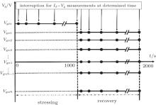
The electrical measurement was implemented by an Agilent B1500A using the conventional stress measure stress (SMS) method with constant voltage stress (CVS). The stress phase was sustained for 1000 s, followed by a recovery phase of 1000 s subsequently (shown in Fig. 2). The threshold voltage was extracted from the Id– Vg curve by the constant current method which was defined as (W/L)× 100 nA. The Id– Vg curve was obtained by interrupting the stress at predetermined time points. The stress temperature was set at 90 ° C. The voltage drop between drain and source (Vds) was set at 50 mV when the Id– Vg curve was extracted.
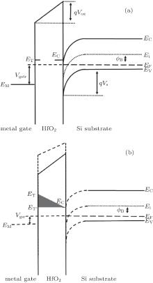
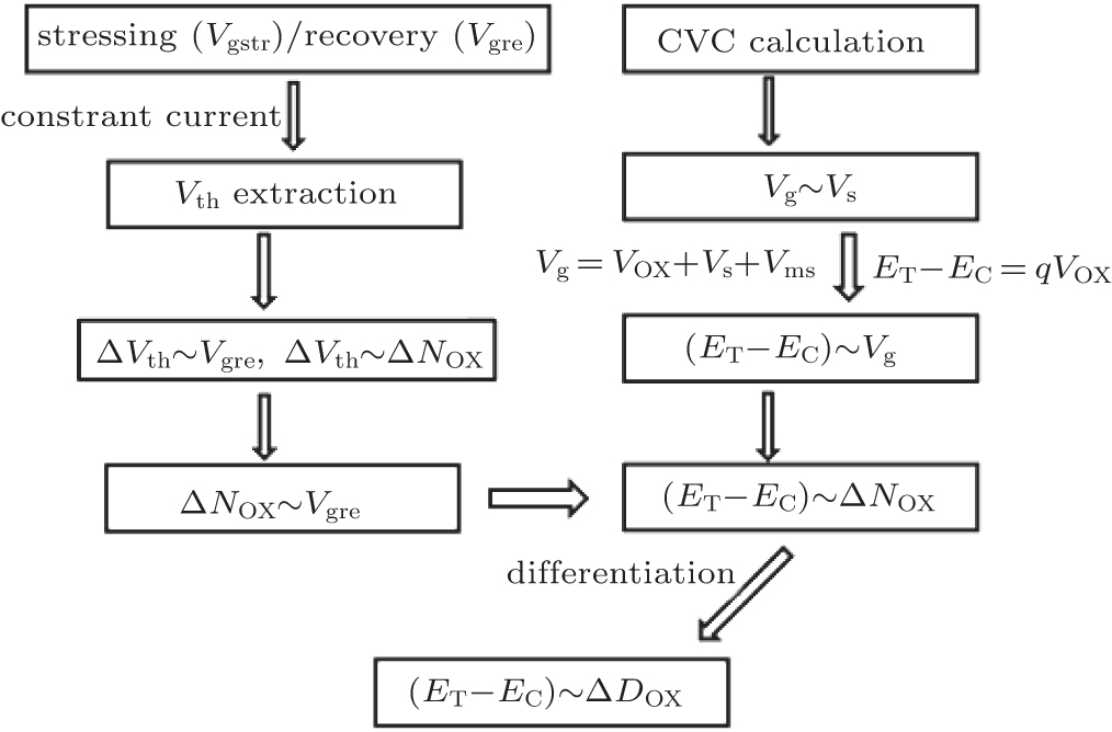
3. Method of energy distribution extractionFigure 3 shows the principle of extracting the energy distribution, ignoring the interfacial layer of silicon dioxide for convenience. Figures 3(a) and 3(b) show the energy band under stress voltage (Vgstr) and the energy band under recovery stress (Vgre), respectively. When the gate voltage changes from stress voltage to recovery stress, a triangular shadow area moves upward to be above the silicon conduction band. Meanwhile, the negative charges in the triangular area will discharge because their energy is above the conduction band of the silicon substrate; therefore, the PBTI degradation (Δ Vth) will recover partially. The more negative the recovery stress is, the more the PBTI degradation recovers. Finally the PBTI degradation will completely recover under enough negative stress for adequate time (shown in Fig. 7(c)).
Based on the capacitance– voltage simulation, the recovery stress is linked to the surface potential of the substrate silicon (Vs).[14] Therefore, the relationship between the recovery stress and ET – EC can be obtained according to


where ET is the trap energy level, EC is the conduction band of the substrate silicon, VOX is the potential drop across the high-k and interfacial layers, Vs is the surface potential drop of the substrate silicon, and Vms is the work function difference of the metal gate and the substrate silicon. Finally, the relationship of ET – EC versus NOX is obtained. The energy distribution (DOX) can be obtained from the differentiation of NOX.
4. Results and discussionFigures 5(a) and 5(b) respectively show Id– Vg and Id– Vd characteristic curves of the tested devices before stress at room temperature. Because of the large gate leakage, Id is negative at the beginning of the Id– Vd curves when Vg becomes larger.
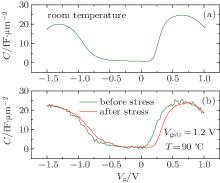
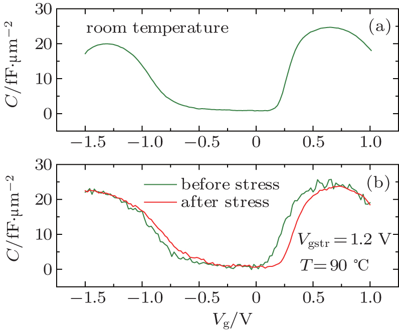
Figure 6(a) shows the C– V characteristic curve at room temperature. Figure 6(b) shows the C– V characteristic curves before and after stress. It can be seen that the C– V characteristic curve after stress shifts positively because of the trapped negative charges compared to the C– V characteristic curve before stress.
Although the purpose is to extract the energy distribution of negative charges, the energy level of traps trapping charges can be reflected. It has been proposed that the interface state is partially responsible for PBTI with respect to the ultrathin high-k/silicon dioxide interlayer structure.[12, 13] In order to verify the generation of the interface state, the sub-threshold swing has been extracted.[15] Almost no variation occurs; so the interface state does not contribute to PBTI.[16]
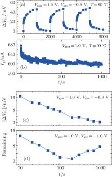
Stress induced defects have been considered to capture electrons to result in the PBTI degradation.[10, 11] Experiments have been conducted to verify this. Figure 7(a) shows three cycles of stressing and recovery, and no additional degradation occurs during the next period of stressing. During stressing, the leakage of the gate electrode decreases monotonously as shown in Fig. 7(b), which can be interpreted by the decrease of the voltage drop across the dielectrics due to the increase of Vth. The degradation can completely recover when a proper negative voltage is used for an adequate period of time, as shown in Fig. 7(c). Based on the aforementioned results, it can be inferred that the PBTI degradation is not caused by stress induced defects but by pre-existing defects. There is another phenomenon: when a larger negative voltage is applied during the recovery phase, the threshold voltage Vth shifts toward negative against its fresh value, which is similar to the negative bias temperature instability (NBTI). Figure 7(d) shows the absolute value of the remaining Vth, and the increase of the tail of the line means that the threshold voltage decreases. It has been reported that hole traps co-exist together with electron traps resulting in electron-discharging.[17]
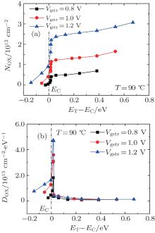
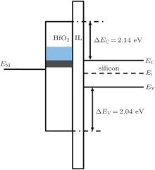
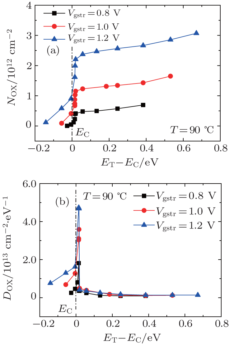
Figures 8(a) and 8(b) show the effective charge density and energy distribution of the negative charges under three different gate stresses, respectively. The conduction band corresponding to silicon is also marked for the convenience of analysis. The energy distribution shows an energy dependence, and the trap band is close to the conduction band of silicon.[18, 19] A maximum value appears at the energy 0.01 eV above the conduction band of silicon. Then the energy density rapidly decreases from two sides. The three lines are completely coincident at the right side of the maximum value. However, an obvious difference appears at the left side of the maximum value. So the stress voltage has a strong impact on the energy distribution in this energy range. With larger stress, more charges are present at the same energy level. It can be inferred that there are two different types of traps. According to x-ray photoelectron spectroscopy (XPS) measurements, the valence band offset between HfO2 and silicon is 2.04 eV, which is smaller than the results measured by other researchers.[20, 21] The reason for this may be the formation of Hf– Si bonds at the interface and different processes. Figure 9 shows the band diagram of silicon/IL/high-k/metal gate stacks. The gray shadow area is the energy range that is strongly influenced by the stress voltage. It indicates that traps in this energy range are not completely active, and can be activated under certain conditions, such as stress voltage, as demonstrated in this work. The oxygen vacancy has been proposed to be the origin of the traps, but contradiction exists about the energy level.[19, 22] So the origin of the traps needs further investigation. The different impact of the stress voltage on the energy distribution should be taken into account when predicting the lifetime of devices by using the acceleration stress test method.
5. ConclusionIn this work, a new method that extracts the energy distribution of PBTI induced charges is proposed. The charges show a strong dependence on energy. A maximum value appears at the energy 0.01 eV above the conduction band of silicon. The stress voltage has a significant impact on the energy distribution below the energy level of the maximum value of energy density.


