


A low-threshold nanolaser based on hybrid plasmonic waveguides at the deep subwavelength scale
[Li Zhi-Quan† , Piao Rui-Qi, Zhao Jing-Jing, Meng Xiao-Yun, Tong Kai]
, Piao Rui-Qi, Zhao Jing-Jing, Meng Xiao-Yun, Tong Kai]
|
|


†Corresponding author. E-mail: lzq54@ysu.edu.cn
*Project supported by the National Natural Science Foundation of China (Grant No. 61172044) and the Natural Science Foundation of Hebei Province, China (Grant No. F2014501150).
A novel nanolaser structure based on a hybrid plasmonic waveguide is proposed and investigated. The coupling between the metal nanowire and the high-index semiconductor nanowire with optical gain leads to a strong field enhancement in the air gap region and low propagation loss, which enables the realization of lasing at the deep subwavelength scale. By optimizing the geometric parameters of the structure, a minimal lasing threshold is achieved while maintaining the capacity of ultra-deep subwavelength mode confinement. Compared with the previous coupled nanowire pair based hybrid plasmonic structure, a lower threshold can be obtained with the same geometric parameters. The proposed nanolaser can be integrated into a miniature chip as a nanoscale light source and has the potential to be widely used in optical communication and optical sensing technology.
With the development of integrated optics and micro-machining technology, the requirement for miniature photonic devices with potential for integration has become urgent. As a result, micro-nanolasers have attracted considerable attention in the field of nano-photonic technology. Semiconductor lasers based on ZnO/CdS nanowires or nanowire arrays enable the scale of microlasers to reach the diffraction limit.[1] However, the minimum size of a semiconductor laser is still limited by the diffraction limit, i.e., (λ /2n)3 for three-dimensional lasers, where λ is the free-space wavelength and n is the refractive index of the dielectric. In recent years, the research of lasers based on plasmonic structures has achieved a major breakthrough in overcoming the diffraction limit[2, 3] by using the surface plasmon (SP), [4] which is a transverse magnetic (TM) polarized surface wave propagating along the metal– dielectric interface. The high field confinement of the surface plasmon has been used to create subwavelength waveguides and cavities for the development of micro-nanolasers.[5, 6]
However, the high loss mainly from metal absorption in plasmonic waveguides limits the propagation length of the plasmonic mode and makes it difficult to form lasing action. Even though some surface plasmon modes, such as long-range surface plasmons, propagate longer distances with lower loss, the corresponding optical confinement becomes much worse.[7] In order to keep a good balance between the propagation loss and the mode confinement, a variety of hybrid plasmonic waveguides for nanolaser applications have been put forward in recent years.[8– 11] Oulton proposed a typical hybrid plasmonic waveguide structure composed of a high-index dielectric nanowire above a metal layer which exhibits low loss and long propagation distance with subwavelength confinement.[12] Then a similar hybrid waveguide consisting of a CdS nanowire on top of a silver substrate separated by an ultra-thin MgF2 buffer layer was investigated.[13] Zhu studied the modal properties of the above hybrid plasmonic waveguide by using the air as the low-index dielectric material and illustrated the coupling mechanism between the surface plasmon mode and the mode of the nanowire waveguide in detail.[14] Compared with the previous structure, [13] a hybrid plasmonic waveguide with an air gap acquires less loss and a lower threshold with the same size, indicating that a buffer layer of lower index (air) can reduce the propagation loss. Based on the above-described structure, Bian proposed several new hybrid plasmonic structures, including a coupled nanowire pair based plasmonic laser structure, [15] a coplanar edge-coupled plasmonic waveguide structure, [16] and so on, [17– 20] which may be used for subwavelength-scale nanolasers with low threshold.
In this paper, we propose a novel surface plasmonic nanolaser based on a metal nanowire/air gap/high-index semiconductor nanowire hybrid structure covered with a low-index dielectric cladding. We analyze the electric field distribution of the proposed structure and calculate the modal characteristics and the lasing threshold by using the finite-element method on the basis of the COMSOL Multiphysics platform. We obtain the optimal size of the nanolaser. The simulation results reveal that our proposed structure has a lower threshold compared to the previous coupled nanowire pair based hybrid plasmonic structure with the same parameters.[15] The structure could be easily integrated with various plasmonic structures and is significant for developing deep subwavelength-scale plasmonic nanolasers with low loss and low threshold.
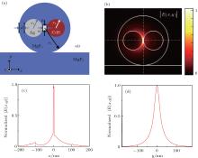
The geometry of the proposed nanolaser is shown in Fig. 1(a). An MgF2 nanowire as the low-index cladding is placed on an MgF2 substrate. An Ag nanowire and a high-index CdS nanowire are symmetrically buried in the MgF2 nanowire. Since a buffer layer of lower index can reduce the propagation loss, [14, 15] an air gap is introduced into the design to achieve lower loss. The air gap is etched between the Ag nanowire and the CdS nanowire. Silver is chosen due to its low absorption coefficient and low propagation loss. The radii of the Ag, CdS and MgF2 nanowires are r1, r2, and r3, respectively (here r1 = r2). The width and height of the air gap are w and h, respectively. The thickness of the MgF2 cladding, d, is fixed at 20 nm, so the radius of the MgF2 nanowire, r3, is equal to 2r1 + w/2 + d. The lasing wavelength is 490 nm. The refractive indices of Ag, MgF2, and CdS are 0.05+ 3.0391i, 1.4, and 2.4, respectively.[16]
 | Fig. 1. (a) Geometry of the proposed plasmonic nanolaser. (b)– (d) Normalized electric field distribution of the fundamental hybrid plasmonic mode of the proposed structure (r1 = r2 = 50 nm, r3 = 122.5 nm, w = 5 nm, h = 15 nm, d = 20 nm). |
From the electric field distribution of the fundamental hybrid plasmonic mode shown in Fig. 1(b) (r1 = r2 = 50 nm, w = 5 nm, h = 15 nm), it is clear that the electric energy is mainly concentrated in the nanometer-size air gap, a portion of which also permeates into the MgF2 material above and below the air gap. In addition, a weak electric field exists around the Ag nanowire and in the CdS nanowire. Compared with the fields in other regions of the proposed structure, the electric field in the air gap is strongly enhanced. Figures 1(c) and 1(d) show the simulated field distributions along the horizontal and the vertical dashed lines in Fig. 1(b), which reflect the field enhancements in the air gap in the horizontal and the vertical directions, respectively. The coupling between the surface plasmon mode at the silver interface and the fundamental mode of the CdS nanowire leads to a strong field enhancement in the gap region, with enough modal overlap in the CdS nanowire to provide the required optical gain, and a high energy confinement is formed.
In the following, we investigate the effect of the geometric parameters on the properties of the nanolaser. The modal properties and the lasing threshold are important indices reflecting the properties of the designed laser. The modal properties include the modal effective index neff, the effective propagation loss α eff, the normalized mode area Aeff/A0, and the confinement factor Γ . The modal effective index and the effective propagation loss are reflected by the real and the imaginary parts of the hybrid waveguide propagation constant over the free-space wavevector, respectively.[14] The normalized mode area is defined as the ratio of the effective mode area to the diffraction-limited mode area and can be expressed as

Here, the effective mode area Aeff is calculated[15] as

where E is the electric field intensity of the hybrid mode. The diffraction-limited mode area A0 is defined as

where λ is the lasing wavelength. The confinement factor Γ is defined as the ratio of the electric energy in the CdS gain nanowire to the total electric energy of the mode and embodies the ability of the gain nanowire to confine the mode field.[15]
We first assume that the air gap height h = 15 nm and investigate the effect of the width of the air gap (w) on the modal properties with different nanowire radii (r1 = r2 = 30 nm, 40 nm, 50 nm, 60 nm, 70 nm). Here w varies from 2 nm to 20 nm. The results shown in Fig. 2 indicate that the modal characteristics of the structures with different nanowire radii show the same trend with increasing air gap width. When the gap width increases from 2 nm to 20 nm, both the modal effective index and the propagation loss decrease because of the weakened coupling between the two nanowires. Moreover, the effective propagation loss gradually levels off at large gap width. This is because when the two nanowires are relatively small compared to the air gap width, more electric energy is confined around the silver nanowire surface. This leads to higher loss, which makes the total loss decrease at a relatively slow rate. With the gap width increasing, the mode area becomes larger and the confinement factor gradually decreases. The result shown in Fig. 2(c) indicates that when r1 and r2 are small (r1 = r2 = 30 nm) and w is very large, the growth of the mode area becomes slow. According to Ref. [15], this is because when the two nanowires are relatively small compared to the gap width, more electric energy is confined around the silver nanowire surface. Therefore, reducing the gap width w can increase the overlapping region between the hybrid mode and the gain medium, achieving smaller mode area and higher confinement factor. The normalized mode area reflects the capacity of the mode confinement. Figure 2(c) shows that when the gap width varies within the range of 2– 20 nm, the normalized mode area always stays below 0.2, indicating that the structure can realize good deep-subwavelength confinement. It is also shown that the hybrid waveguide with larger nanowire radii exhibits lower propagation loss, smaller effective mode area, and higher confinement factor simultaneously.
 | Fig. 2. The modal properties of the fundamental hybrid plasmonic mode with different w for the cases of nanowire radii r1 = r2 = 30 nm, 40 nm, 50 nm, 60 nm, 70 nm (h = 15 nm, d = 20 nm, r3 = 2r1 + w/2 + d): (a) modal effective index neff, (b) effective propagation loss α eff, (c) normalized mode area Aeff/A0, (d) confinement factor Γ . |
To further evaluate the performance of the presented structure, we investigate the dependence of the lasing threshold of the fundamental hybrid plasmonic mode on the gap width w (shown in Fig. 3). The pump threshold for lasing is related to the nanowire length L and the end facet reflectivity R. Here, we set the nanowire length L to be 30 μ m. The reflectivity R is calculated by the following equation:

In this paper, we do not consider the effect of the MgF2 cladding on the end facet reflectivity and simply estimate the reflectivity to illustrate the influence of the geometric parameters on the lasing threshold. The lasing threshold is calculated[14] by

where k0 = 2π /λ , nwire is the refractive index of the gain nanowire, and neff/nwire is the enhancement part of the modal effective index.
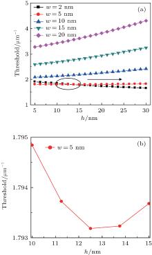
 | Fig. 3. Dependence of lasing threshold of the fundamental hybrid plasmonic mode on w for the cases of nanowire radii r1 = r2 = 30 nm, 40 nm, 50 nm, 60 nm, 70 nm (h = 15 nm, d = 20 nm, r3 = 2r1 + w/2 + d): (a) the complete trend for thresholds with the chosen parameters, (b) enlarged plot for the circled region in panel (a). |
Figure 3(a) shows the complete trend for thresholds with the chosen parameters, and figure 3(b) is the enlarged plot for the corresponding region in Fig. 3(a). As shown in Figs. 3(a) and 3(b), when the air gap width increases from 2 nm to 20 nm, the threshold firstly decreases before increasing for large Ag and CdS nanowires (e.g., r1 = r2 = 50 nm, 60 nm, 70 nm), so a minimum threshold can be obtained at a certain air gap width. In Fig. 3(a), for the waveguide with small nanowire radii (e.g., r1 = r2 = 30 nm, 40 nm), due to relatively high propagation loss and rapidly reduced mode overlap in the gain nanowire, the lasing threshold shows a monotonic increasing trend as the gap width increases. Particularly, when the nanowire radius is 30 nm, the threshold increases sharply. Figure 3 also indicates that the structure with two larger nanowires achieves a lower threshold. However, considering the limitation of the actual size and the adverse effect of other plasmonic modes for practical applications, too large a nanowire should not be chosen. Here, the adverse effect[14] is that when the nanowire radius is not sufficiently small, the perturbed supermode with a much larger mode area will become the lasing mode, which is disadvantageous for obtaining the desired deep subwavelength scale plasmonic laser.
Furthermore, the influence of the air gap height h on the properties of the proposed laser is investigated. Here, the radii of the two nanowires r1, r2 are fixed at 50 nm and the air gap width w is chosen to be 2 nm, 5 nm, 10 nm, 15 nm, and 20 nm, respectively. The air gap height h is set within the range of 5– 30 nm. From the simulation results shown in Figs. 4(a) and 4(b), it is revealed that the modal effective index and the propagation loss decrease continually due to the increased air gap area with increasing gap height h for all chosen gap widths. When the gap width is relatively large, the propagation loss decreases very slowly. This is because the coupling between the two nanowires is relatively weak in this case, and the effect of the change of the air gap area on the propagation loss is weakened correspondingly. Figure 4(c) illustrates that a smaller mode area can be achieved by reducing the gap height. However, when the air gap is very narrow (e. g., w = 2 nm, 5 nm), enlarging h makes the coupling interaction become much stronger and the electric energy is more concentrated in the air gap, consequently resulting in the decreased effective mode area. It is also observed in Fig. 4(c) that for the chosen sizes, the normalized mode area is always below 0.25, indicating deep-subwavelength mode confinement. Figure 4(d) shows that reducing the gap height results in higher confinement factor as well.
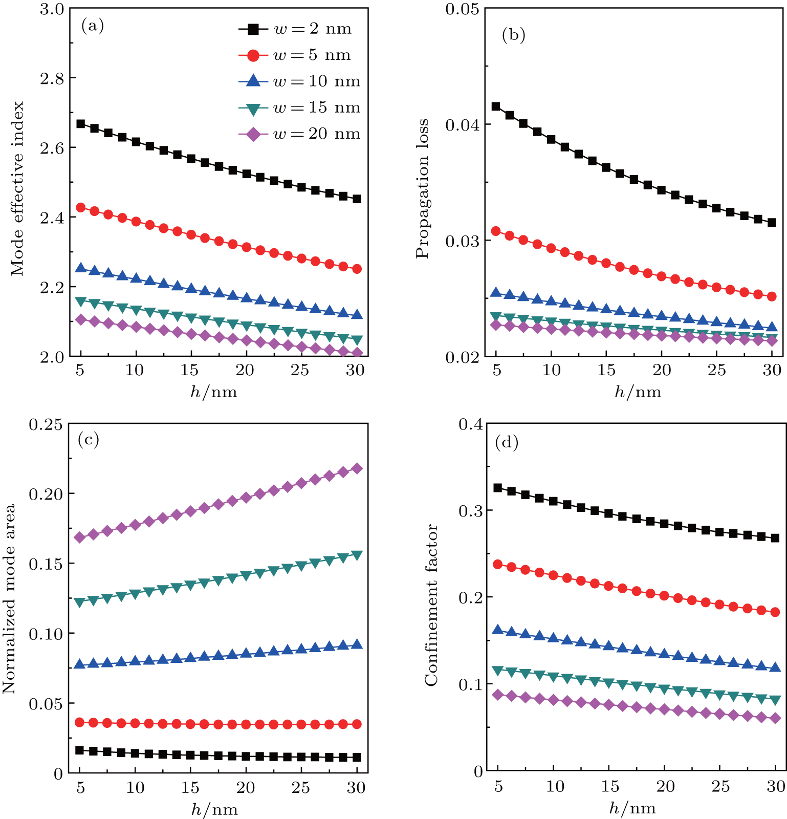 | Fig. 4. The modal properties of the fundamental hybrid plasmonic mode with different h for the cases of gap width w = 2 nm, 5 nm, 10 nm, 15 nm, 20 nm (r1 = r2 = 50 nm, d = 20 nm, r3 = 2r1 + w/2 + d): (a) modal effective index neff, (b) effective propagation loss α eff, (c) normalized mode area Aeff/A0, (d) confinement factor Γ . |
On the basis of the above research of the modal properties, we explore the effect of the air gap height h on the lasing threshold. From Fig. 5, it is obvious that the thresholds of the structures with different w show different trends as h increases. When the air gap is relatively narrow (e.g., w = 2 nm), reduced threshold can be observed at larger gap height. With a large overlap between the hybrid mode and the gain medium, enough gain could be provided to compensate the loss, which causes the reduced threshold as the loss sharply decreases. Whereas for wide air gaps (e.g., w = 10 nm, 15 nm, 20 nm), the pumping threshold becomes higher and higher with increasing h. In this case, the insufficient overlap region in the gain medium rapidly becomes smaller due to the increased h, and the lasing threshold gradually increases in spite of the slowly decreased propagation loss. When w is fixed at 5 nm, the threshold firstly decreases before increasing as h increases, indicating a minimum threshold achieved at h = 12.5 nm (shown in Fig. 5(b)).
 | Fig. 5. Dependence of lasing threshold of the fundamental hybrid plasmonic mode on h for the cases of gap width w = 2 nm, 5 nm, 10 nm, 15 nm, 20 nm (r1 = r2 = 50 nm, d = 20 nm, r3 = 2r1 + w/2 + d): (a) the thresholds for all chosen parameters, (b) enlarged plot for the circled region in panel (a). |
Figure 6 shows the comparison of lasing threshold between the present hybrid plasmonic waveguide and the previous coupled nanowire pairs based hybrid plasmonic structure.[15] According to Ref. [15], the previous hybrid plasmonic structure can realize deep-subwavelength mode confinement as well. However, the proposed structure shows much lower threshold than the previous hybrid plasmonic structure when they have the same gap width and nanowire radii (especially for large gap width), which is beneficial for realizing low-threshold lasing.
 | Fig. 6. Comparison of lasing threshold between the present hybrid plasmonic waveguide and the previous hybrid plasmonic waveguide[15] with different gap width w for the cases of nanowire radii r2 = 40 nm, 50 nm, 60 nm (h = 30 nm, d = 20 nm, r3 = 2r1 + w/2 + d). |
Although the proposed structure can make the optical energy confined in the gap region to realize the subwavelength confinement, there is a disadvantage for the optical gain in the CdS nanowire. For a small gap width (e.g., w = 2 nm), the overlap of the hybrid mode and the gain region is enough to provide the optical gain. However, when the gap width is relatively large (e.g., w = 20 nm), the weak modal overlap in the gain medium results in a large threshold, which is undesirable in practical applications.
Above all, the characteristic of the proposed structure can be regulated by changing the geometric parameters w, h, r1, and r2. If the radii of the two nanowires r1, r2 are fixed at 50 nm, the ultra-deep subwavelength lasing with the minimum pump threshold could be realized by respectively setting the width and the height of the air gap at 2 nm and 30 nm. In this case, the lasing threshold and the normalized mode area can reach 1.65 μ m− 1 and 0.01, respectively.
The fabrication of the designed nanolaser may be a challenge, but is not entirely impossible with the development of nano-fabrication technology. Nano-fabrication techniques such as the focused ion-beam (FIB), dry etching, annealing, and various material deposition techniques can be used to fabricate the waveguide.[8, 17, 21]
We propose a new type of nanolaser structure based on a hybrid plasmonic waveguide which enables deep-subwavelength scale lasing with low propagation loss. We investigate the effect of the width and height of the air gap and the nanowire radius on the nanolaser’ s properties. It is demonstrated that by appropriately adjusting these parameters, the lasing threshold can be significantly reduced while maintaining the capacity of ultra-deep subwavelength mode confinement. We obtain the optimal size of the nanolaser. Compared with the previous coupled nanowire pair based hybrid plasmonic structure, [15] a lower threshold is achieved for the proposed nanolaser with the same geometric parameters. The proposed hybrid plasmonic waveguide structure provides a theoretical basis and research ideas for the development of a new generation of nanolaser. It could be easily integrated with various nanophotonic devices and shows potential for application in many fields such as optical sensing, optical communication, and so on.
| 1 |
|
| 2 |
|
| 3 |
|
| 4 |
|
| 5 |
|
| 6 |
|
| 7 |
|
| 8 |
|
| 9 |
|
| 10 |
|
| 11 |
|
| 12 |
|
| 13 |
|
| 14 |
|
| 15 |
|
| 16 |
|
| 17 |
|
| 18 |
|
| 19 |
|
| 20 |
|
| 21 |
|