

Au and Ti induced charge redistributions on monolayer WS2
[Zhu Hui-Lia) , Yang Wei-Huangb) , Wu Ya-Pingc) , Lin Weic) , Kang Jun-Yongc) , Zhou Chang-Jie†a)  ]
]
]
|
|


†Corresponding author. E-mail: zhoucj@jmu.edu.cn
*Project supported by the National Natural Science Foundation of China (Grant Nos. 91321102, 11304257, and 61227009), the Natural Science Foundation of Fujian Province, China (Grant Nos. 2011J05006, 2009J05149, and 2014J01026), the Foundation from Department of Education of Fujian Province, China (Grant No. JA09146), Huang Hui Zhen Foundation of Jimei University, China (Grant No. ZC2010014), and the Scientific Research Foundation of Jimei University, China (Grant Nos. ZQ2011008 and ZQ2009004).
By using the first-principles calculations, structural and electronic properties of Au and Ti adsorbed WS2 monolayers are studied systematically. For Au-adsorbed WS2, metallic interface states are induced in the middle of the band gap across the Fermi level. These interface states origin mainly from the Au-6s states. As to the Ti adsorbed WS2, some delocalized interface states appear and follow the bottom of conduction band. The Fermi level arises into the conduction band and leads to the n-type conducting behavior. The n-type interface states are found mainly come from the Ti-3d and W-5d states due to the strong Ti–S hybridization. The related partial charge densities between Ti and S atoms are much higher and increased by an order of magnitude as compared with that of Au-adsorbed WS2. Therefore, the electron transport across the Ti-adsorbed WS2 system is mainly by the resonant transport, which would further enhances the electronic transparency when monolayer WS2 contacts with metal Ti. These investigations are of significant importance in understanding the electronic properties of metal atom adsorption on monolayer WS2 and offer valuable references for the design and fabrication of 2D nanodevices.
Since the discovery of graphene, two-dimensional (2D) nanomaterials have caused significant attention of the scientific community because of their attractive interest in nano-science and condensed matter physics.[1, 2] Similar to graphene, layered transition metal dichalcogenides (TMDs) with strong in-plane covalent bonding and weak out-of-plane van der Walls bonding have also captured people’ s focus. Among various TMDs, individual monolayers of TMDs such as MoS2 and WS2 have recently been intensively studied[3– 22] as 2D semiconductor crystals with direct band gap in the visible spectrum, which makes them even more attractive than graphene and boron nitride films and will guarantee a promising future as the candidate of next-generation nanoelectronics, spintronics, valleytronics, catalysis, and optoelectronics. To achieve the goal, significant attempts have been made to fabricate monolayers of MoS2 and WS2, such as mechanical and chemical exfoliation, [3– 6] chemical vapor deposition (CVD), [7, 8] microwave-assisted method, [9] and sulfurization method.[10] To date, by using a controlled thermal reduction-sulfurization method, large-area (∼ 1 cm2) WS2 sheets with the thickness ranging from monolayers to a few layers have been successfully synthesized.[10] Furthermore, many inspiring physicochemical properties have also been examined, including the transport, [11] photocurrent, [12] photoluminescence, [3, 4, 13] and stiffness.[14] For applicability of these novel materials, a perfect Ohmic contact on monolayer TMDs, such as monolayer WS2, with high electronic transparency is needed.
Among transition metals with d orbitals, Au and Ti are identified as the suitable candidates, because they fulfill the criteria required of a good contact material in electronics such as matched lattice constant, high conductivity, and chemical, thermal, and electrical stability. Moreover, Riley’ s experimental results[23] indicated that layered WS2 devices exhibit straightforward Ohmic characteristics with sputtered Ti/Au (10/80 nm) contacts. Meanwhile, in field-effect transistors based on the multilayer WS2, researchers observed the Schottky barriers (SBs) in the Au/WS2 contacts from the non-linear characteristics of the output curve.[24] Apparently, the underlying mechanism regarding the metal contacts on monolayer TMDs, especially the interaction with monolayer WS2 (M– WS2), is lacking at present. Furthermore, due to a high surface-to-volume ratio, the electrical properties of atomically thin nanomaterials can be significantly perturbed even by submonolayer adsorption of metal atoms. Therefore, a systematic study on the electronic properties of metal Au and Ti adsorbed monolayer WS2 is desired from the theoretical point of view.
In this work, structure and electronic properties of Au and Ti adsorbed M– WS2 are studied systematically by using the first-principles DFT calculations. Energy band structures are computed to ascertain the electronic interface states. Total and partial density of states (DOSs) are calculated to understand the contributions of different atoms to these interface states. Furthermore, the deformation charge densities are introduced to depict the charge redistribution associated with the adsorption of Au and Ti atoms in real space. Finally, the related partial charge densities are calculated and analyzed in detail to gain the insight into the electron transition probability between the adsorbed metal atoms and the underlying M– WS2 layer.
In the present study, structural and electronic properties of Au and Ti adsorbed M– WS2 are studied by the first-principles calculations within the framework of the local density approximation (LDA), [25– 28] using the plane-wave density functional theory Vienna ab initio simulation package (VASP).[29– 31] The 2 × 2 supercells (4 W and 8 S atoms) are used to simulate the individual M– WS2, and in order to avoid interlayer interactions, the distance between monolayers is set to be larger than 20 Å . The plane-wave cutoff energy is set at 500 eV. A Monkhorst– Pack k-point mesh of 8 × 8 × 1 is used to calculate the Brillouin zone integration.[32] The W-5d6s, S-3s3p, Au-5d6s, and Ti-3d4s are employed as the valence electrons. Structural optimizations are carried out by relaxing all the atomic geometries using the conjugate gradient algorithm. The forces on all the atoms are converged within 0.01 eV/Å .
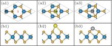
In the relaxed structure of pristine M– WS2, as shown in Figs. 1(a1) and 1(b1), the planar projection shows a perfect hexagonal lattice of S atoms, with interleaved W atoms coordinated by the S atoms in a trigonal prismatic arrangement. The structure is similar to that of MoS2 and some of the other dichalcogenides. The optimized lattice constant of pristine M– WS2 is about 3.13 Å in our calculation, which agrees well with the experimental value of 3.15 Å .[33] The length of W– S bond and S– W– S angle between the nearest neighbor S atoms is obtained to be about 2.39 Å and 81.8° , respectively, well consistent with the previous calculations.[34]
 | Fig. 1. Top views of the relaxed pristine (a1), Au (a2), and Ti (a3) adsorbed M– WS2. Side views of the relaxed pristine (b1), Au (b2), and Ti (b3) adsorbed M– WS2. The big blue and small yellow spheres represent the W and S atoms, respectively. The big yellow and big gray spheres represent the Au and Ti atoms, respectively. Sites 1 and 2 represent the six equivalent hollow site “ H” and the top site “ T” , respectively. |
Since M– WS2 belongs to the P
Figures 1(a2) and 1(b2) are respectively the top and side views of the relaxed Au adsorbed M– WS2. The relaxation calculations show that Au– S bond is 2.62 Å , which is about 0.16 Å longer than the total lengths of the S and Au covalent radii. The longer bond length will partly suppress the efficient overlap of wave functon between Au and underlying M– WS2. Figures 1(a3) and 1(b3) are respectively the top and side views of the relaxed Ti adsorbed M– WS2. Obviously different from the Au/M– WS2 system, Ti– S bond is calculated to be 2.17 Å , about 0.21 Å shorter than the total lengths of the S and Ti covalent radii. The shorter bond length indicates the favorable conditions for a large wave function overlap between Ti and underlying M– WS2. The vertical distance between the Au and the upmost S of M– WS2 is obtained to be 1.91 Å , about 0.92 Å longer than that of Ti/M– WS2 system. Therefore, Ti atom adsorbed on “ H” site is much more stable than that of Au atom and indicates the largely wave function overlaping and strong interaction between Ti atom and underlying M– WS2 layers.
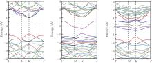
To ascertain the difference of the electronic states of Au and Ti adsorbed M– WS2, the energy band structures are simulated as shown in Figs. 2(b) and 2(c), respectively. For comparison, energy band structure of the pristine M– WS2 is also calculated as shown in Fig. 2(a). The LDA calculated direct band gap of pristine M– WS2 between the top of valance band (EV) and the bottom of conduction band (EC) at K point is about 1.98 eV, as shown in Fig. 2(a), which is 0.13 eV wider than the GGA calculation[34] and agrees well with the experimetal result of about 2.0 eV.[13, 35– 37] As the adsorption of Au and Ti atoms, the energy band structures are clearly influenced as shown in Figs. 2(b) and 2(c). It is found that the Au adsorption induces a single energy level in the middle of the energy band gap and the Fermi level (EF) acrosses the single splitted energy level, indicating the formation of the metallic interface states. The energy region from the Fermi level to EC and EV is about 1.07 and 0.93 eV, respectively. The wide energy regions indicates that high SBs may be formed when metal Au contacts with M– WS2. However, for Ti/M– WS2 system, some interface states appear in the band gap and follow the bottom of conduction band of the pristine M– WS2. The appearance of this kind of delocalized interface states is mainly attributed to the splitting and ourspreads of the conduction band. A narrow surface band gap of about 0.81 eV exists above the top of the valence band of the pristine M– WS2. Moreover, the Fermi level arises into the conduction band deeply, which leads to the occupation of partial interface states under the Fermi level. Therefore, the Ti adsorbed M– WS2 shows the n-type conduction characterized behavior, which is in favour of the formation of Ohmic contact when metal Ti contacts with M– WS2.
 | Fig. 2. Energy band structures of the pristine (a), Au (b), and Ti (c) adsorbed M– WS2 plotted along the Γ – M– K– Γ in the Brillouin zone. The Fermi level is located at 0 eV and indicated by the dotted line. |
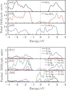
In order to understand the contributions of different atoms to these interface states, total and partial DOSs are calculated, as shown in Fig. 3. Au-adsorbed M– WS2 shows that the total DOSs of the conduction and valence bands are almost the same as that of the pristine M– WS2. Some low interface states emerge in the center of the band gap, leaving two suface band gaps on either side of these states, as shown in Fig. 3(a2). Moreover, these interface states are crossed exactly by the Fermi level, indicating the metallic conduction. While for the total DOSs of Ti adsorbed M– WS2, as shown in Fig. 3(a3), it could be found that the Ti adsorption modifies the electronic states near the EF much more than that of the Au adsorption. In Ti/M– WS2 system, the Fermi level is shifted upwards by 0.56 eV above the EC. The total DOSs at the Fermi level is much higher than that in Au/M– WS2 system. Furthermore, the overlaping of the total DOSs among the conduction band reflects an increase in the dispersion of the corresponding bands and suggests the formation of delocalized states at the interface of Ti and underlying M– WS2.
 | Fig. 3. Total ((a1)– (a3)) and partial ((b1)– (b3)) DOSs of the pristine, Au and Ti adsorbed M– WS2. The Fermi level is located at 0 eV and indicated by the dotted line. |
Partical DOSs of W, S, Au, and Ti atoms are further presented for the pristine, Au, and Ti adsorbed M– WS2, as shown in Figs. 3(b1)– 3(b3). The bottom of the conduction band and the top of the valence band of the pristine M– WS2 are dominated by W-5d states, while the S-3p states play a minor role. For the Au/M– WS2 system, the observed metallic interface states origin mainly from the Au-6s states, with S-3s and S-3p states making a minor contribution, indicating the weak sp orbital coupling between Au and S atom. Energy distribution of W-5d and S-3p states stay almost the same in the Au/M– WS2 system as compared with that of the pristine M– WS2. This fact further indicates the weak coupling between the adsorbed Au atom and the W and S atoms despit that the Au-5d state distributes in the same energy region of the valence band. For the Ti/M– WS2 system, the observed delocalized and n-type metallic conduction interface states origin mainly from the Ti-3d and W-5d states, while the S-3p states only play a minor role. Furthermore, energy distribution of W-5d and S-3p states shift downwards to the lower energy level and the energy range of the conduciton band become obviously wider as compared with that of the pristine M– WS2. Thinking about the hardly bonding behavior between Ti and W atoms, the formation of these interface states are definitely associated with the strong Ti– S hybridization and which further induces the shift and splitting of the W-5d states.
Appearently, the striking different origin of the interface stats near the Fermi level for the Au/M– WS2 and Ti/M– WS2 systems is definitely associated with the intensity of the Au– S and Ti– S mixing. A higher DOSs near the Fermi level forming the delocalized states would allow more electrons to transfer between the Ti and underlying M– WS2 as compared with that of Au/M– WS2 system.
To further depict the interaction and the charge redistribution between adsorbed metal atoms and underlying M– WS2 in real space, we introduce the deformation charge density Δ ρ (r) via the expression: 
where ρ (r) and 
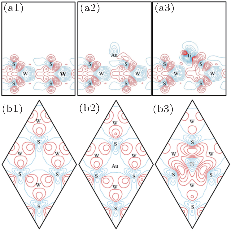 | Fig. 4. The vertical ((a1)– (a3)) and lateral ((b1)– (b3)) sections of deformation charge densities of the pristine, Au and Ti adsorbed M– WS2. The vertical sections contain the Au– S and Ti– S bonds. The lateral sections contain the upmost S atoms. The contours interval is 0.004 e/Å 3, positive contours are shown as red solid lines, and negative contours as blue dashed lines. |
The related partial charge densities are further calculated and analyzed in detail to gain insight into the electron transition probability between the adsorbed metal atoms and the underlying M– WS2. Since the partial DOSs around the Fermi level play a more crucial role in the electronic transparency, the partial charge densities in the energy range EF − 0.1 eV < EF < EF + 0.1 eV are calculated, as shown in Fig. 5. For the Au/M– WS2 system, the partial charge densities mainly distribute around the Au, nearest neighbor S and its bonding W atoms. The partial charge densities between the Au and the nearest neighbor S atom are very small. Further considering the longer Au– S bond, the electron transport across the Au/M– WS2 system is mainly of a tunneling nature. In striking constrast to the Au/M– WS2 system, the partial charge densities mainly distribute around the Ti, the nearest neighbor W, the nearest neighbor S, and its bonding W atoms. The partial charge densities between Ti and the nearest neighbor S atom are much higher and increases by an order of magnitude as compared with that of Au/M– WS2 system. Further considering the shorter Ti– S bond, the electron transport across the Ti/M– WS2 system is mainly through a resonant transport. The significantly accumulated partial charge densities near EF in the Ti/M– WS2 system will definitely enhance the electron transition probability.
 | Fig. 5. The vertical ((a1), (a2)) and lateral ((b1), (b2)) sections of partial charge densities of Au and Ti adsorbed M– WS2 in the energy range EF − 0.1 eV < EF < EF + 0.1 eV. The vertical sections contain the Au– S and Ti– S bonds. The lateral sections contain the upmost S atoms. The contours interval is 0.0005 e/Å 3. |
In conclusion, using the first-principles DFT calculations, the structural and electronic properties of Au and Ti adsorbed M– WS2 are studied systematically. The relaxation calculations show that Ti– S bond is much shorter than Au– S bond, and the shorter bond length indicates the favorable conditions for a large wave function overlap between Ti and underlying M– WS2. According to the results of energy band structures and total DOSs, some metallic interface states are induced in the middle of the band gap with the Fermi level crossing the split level by the adsorption of Au atom. For the Ti/M– WS2 system, and some delocalized interface states appear and follow the bottom of conduction band. The Fermi level arises into the conduction band deeply, which leads to the n-type conducting behavior and is in favor of the formation of Ohmic contact. Partial DOSs are calculated to understand the contributions of different atoms. For Au/M– WS2, the interface states origin mainly from Au-6s states. For Ti/M– WS2, the n-type metallic interface states origin mainly from Ti-3d and W-5d states, with S-3p states playing a minor role, which is associated with the strong Ti– S hybridization. The related partial charge densities are calculated and analyzed to gain insight into the electron transition probability between the adsorbed metal atom and the underlying M– WS2. Charge densities between Ti and S atoms are much higher and increase by an order of magnitude as compared with that of Au/M– WS2 system. Therefore, the electron transport across the Ti/M– WS2 system mainly through a resonant transport and which would further enhance the electronic transparency. These investigations are of significant importance in understanding the electronic properties of metal atom adsorption on M– WS2 and offer valuable references for the design and fabrication of 2D nanodevices.
| 1 |
|
| 2 |
|
| 3 |
|
| 4 |
|
| 5 |
|
| 6 |
|
| 7 |
|
| 8 |
|
| 9 |
|
| 10 |
|
| 11 |
|
| 12 |
|
| 13 |
|
| 14 |
|
| 15 |
|
| 16 |
|
| 17 |
|
| 18 |
|
| 19 |
|
| 20 |
|
| 21 |
|
| 22 |
|
| 23 |
|
| 24 |
|
| 25 |
|
| 26 |
|
| 27 |
|
| 28 |
|
| 29 |
|
| 30 |
|
| 31 |
|
| 32 |
|
| 33 |
|
| 34 |
|
| 35 |
|
| 36 |
|
| 37 |
|