Nondestructive measurement of thermal contact resistance for the power vertical double-diffused metal-oxide-semiconductor
[Li Rui, Guo Chun-Sheng† , Feng Shi-Wei, Shi Lei, Zhu Hui, Wang Lin]
, Feng Shi-Wei, Shi Lei, Zhu Hui, Wang Lin]
|
|


†Corresponding author. E-mail: guocs@bjut.edu.cn
*Project supported by the National Natural Science Foundation of China (Grant No. 61204081).
To obtain thermal contact resistance (TCR) between the vertical double-diffused metal-oxide-semiconductor (VDMOS) and the heat sink, we derived the relationship between the total thermal resistance and the contact force imposed on the VDMOS. The total thermal resistance from the chip to the heat sink is measured under different contact forces, and the TCR can be extracted nondestructively from the derived relationship. Finally, the experimental results are compared with the simulation results.

The TCR has been measured by two methods:[4] the temperature difference linear extrapolation method and the photo thermal measurement method. However, both methods have their own disadvantages. For the former, an error will be caused when the temperature difference at the interface is small. For the latter, the photo light path is susceptible to the surrounding environment.[4] Other methods such as the transient method[8] and the function method have been developed to measure the TCR. However, the transient electrical method becomes invalid when a material with high thermal resistance and low thermal capacitance is located between two high thermal resistance materials.[9]
In this work, we develop a method based on the relationship between the total thermal resistance and the contact force to derive the TCR nondestructively. Moreover, a simulation of TCR is established to verify the model.
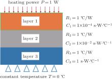
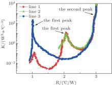
Normally, the contribution of each component to the total thermal resistance can be obtained from the differential structure function curve.[10, 11] It requires that the thermal capacity of a layer is larger than that of the upper layer by two or more orders of magnitude.[9] The three-layer material model is constructed, as shown in Fig. 1. Each layer has the same thermal resistance but different thermal capacitances. The thermal capacity of three layers are C1 = 1 × 10− 4 s· W· ° C− 1, C2 = 1 × 10− 2 s· W· ° C− 1, and C3 = 1 s· W· ° C− 1, respectively. The differential structure function curve from the thermal simulation is represented by line 1 in Fig. 2. The abscissa represents the thermal resistance and the vertical axis represents thermal capacity. If the layer order is reconstructed as layer 213 or layer 132, the differential structure function curve becomes line 2 or line 3, respectively. It can be seen that there are three peaks on line 1, representing the thermal resistances of different layers. However, there are just two peaks on line 2 and line 3 is missing one layer thermal resistance, so the accuracy of the structure function method depends on the arrangement of layers with different thermal capacitance.
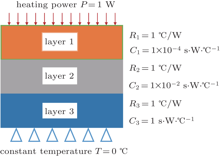 | Fig. 1. Schematic diagram of a three-layer semiconductor. |
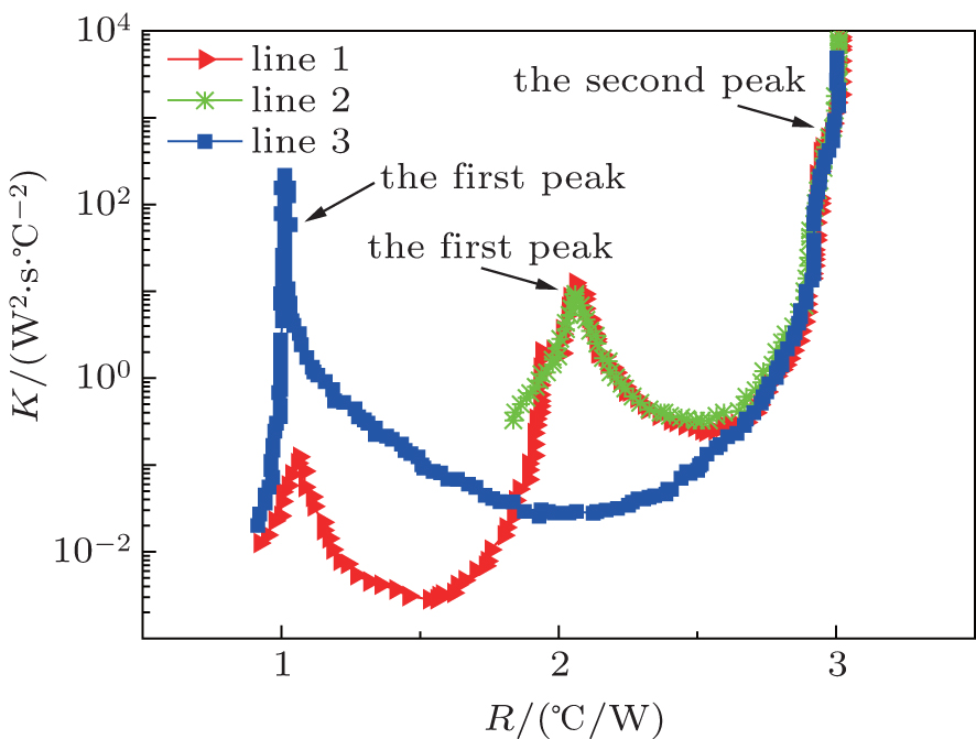 | Fig. 2. Differential structure function curves of the transient chip temperature for models with different thermal capacitance parameters. |
Because the TCR is dependent on the contact force, we develop a method to derive the TCR from its relationship with the contact force. The total thermal resistance along the heat dissipation paths is the sum of the thermal resistance between the chip and case Rjc, the TCR Rth, and the thermal resistance of the heat sink Rf as follows:[12]

and the real contact area Ac and force F can be calculated by the following equations:[12– 14]


where Am represents the theoretical contact area, z is the height of contact peak without contact power, d is the height of the contact peak under contact power, H is the equivalent hardness, m is the equivalent slope of the contact peak, and η is the density of the contact peak, respectively. The integration means the mathematical expectation of the total number of contact peaks in the contact area Am. Thus, a linear relationship between Ac and F can be derived from Eqs. (2) and (3)

which demonstrates that the real contact area is dependent on the contact force. Furthermore, the thermal contact conductance has an exponential dependence on the real contact area.[12] The thermal resistance is equal to the reciprocal of the thermal conductance. The Rth can be rewritten in the following equation with a negative exponential of Ac

In addition, Rth follows an exponential decay with F

As the contact force increases, the deformation of the contact surface will increase, giving rise to the increase of the real contact area, and hence the reduction of TCR. When the deformation reaches a maximum value at a sufficiently large force, the minimum TCR will be obtained which is equal to Rth(o). It will remain unchanged even if the contact force continues to increase[12], so equation (1) becomes

In addition, The total thermal resistance can be expressed by the exponential equation as

and the TCR is

Therefore, the exponential decay function of TCR is developed, and the TCR through the contact force can be obtained by fitting the experimental data of Rja and F.
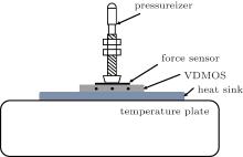
The DUT (device under test) consisting of a high-power VDMOS device (International Rectifier, El Segundo, CA) and an aluminum heat sink (10-cm long, 4-cm wide, and 0.4-cm thick) is placed on a temperature plate in Fig. 3. The pressurizer controls the contact force between the VDMOS and the heat sink. The force is measured by the force sensor. Then a thermal analyzer is used (Model Phase11, Analysis Tech, Wakefield, MA) to measure the Rja under different contact forces F within the range 30– 800 N.
 | Fig. 3. The DUT consists of a pressurizer, force sensor, VDMOS device, and heat sink. |
The total thermal resistance Rja is measured at different contact forces F. The Rth at different contact forces can be extracted nondestructively from the fitting of Rja– F curves, which follows the negative exponential relationship with F as

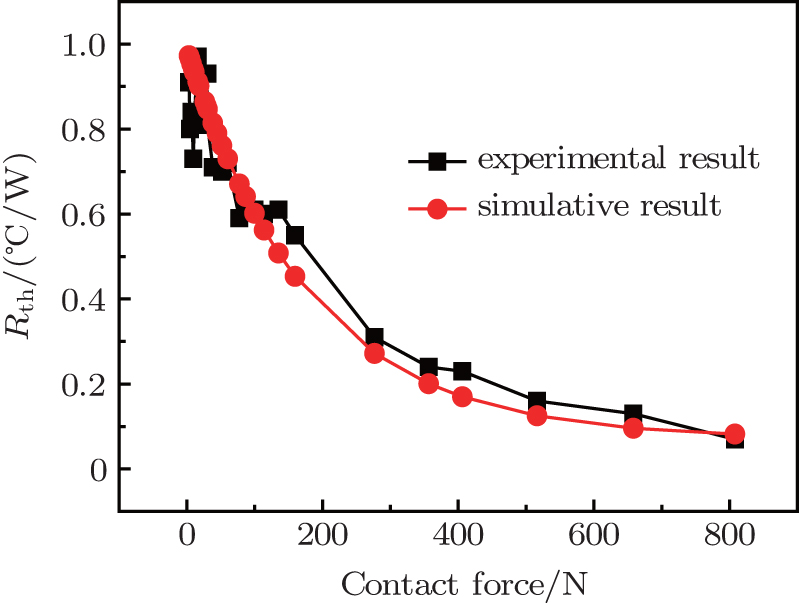
and the relationship curve of Rth and F is shown in Fig. 4.
 | Fig. 4. Schematic diagram of the TCR in the ICEPAK thermal simulation software. |
The TCR-F simulation is performed using the ICEPAK software to verify the accuracy of the method. The real contact areas at different contract forces are calculated according to Eqs. (2), (3), and (5). They are utilized by the TCR model in the ICEPAK software (ANSYS, Canonsburg, PA).
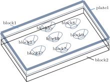
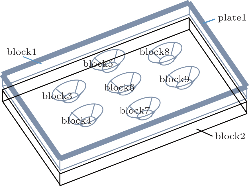
The TCR model is given in Fig. 5, with the plate 1 representing the heat generator, block 1 representing the device package, block 2 representing the heat sink up surface, and block 3 to block 9 representing the peak models of the package rough surface, respectively.[13]
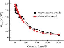
 | Fig. 5. Comparison of the Rth versus F curves from simulation and experimental results. |
The heating power and ambient temperature are set to be 10 W and 20 ° C, respectively. The thermal resistance can be calculated by dividing the interface temperature difference by the heating power

The experimental and simulation results are listed in Table 1 and the two results are in good agreement with each other as shown in Fig. 4.
| Table 1. Samples of the simulation and experimental data. |
A nondestructive measurement method is presented to measure the TCR between the VDMOS and an aluminum heat sink. The total thermal resistance from the chip to the heat sink is measured at different contact forces from 3 N to 800 N. The relationship between the TCR and contact force is derived and the underlying physical mechanism is analyzed. We obtain that the deformation of the contact interface increases as the contact force increases, the TCRs follow an exponential decay with the contact forces, and the experiment results and simulation results are consistent with each other.
| 1 |
|
| 2 |
|
| 3 |
|
| 4 |
|
| 5 |
|
| 6 |
|
| 7 |
|
| 8 |
|
| 9 |
|
| 10 |
|
| 11 |
|
| 12 |
|
| 13 |
|
| 14 |
|
| 15 |
|
| 16 |
|
| 17 |
|