


Subthreshold behavior of AlInSb/InSb high electron mobility transistors
[Theodore Chandra S.† , Balamurugan N. B., Lakshmi Priya G., Manikandan S.]
, Balamurugan N. B., Lakshmi Priya G., Manikandan S.]
|
|


†Corresponding author. E-mail: theodore@tce.edu
*Project supported by the Council of Scientific & Industrial Research (CSIR), Government of India under the SRF Scheme (Sanction Letter No: 08/237(0005)/2012-EMR-I).
We propose a scaling theory for single gate AlInSb/InSb high electron mobility transistors (HEMTs) by solving the two-dimensional (2D) Poisson equation. In our model, the effective conductive path effect (ECPE) is taken into account to overcome the problems arising from the device scaling. The potential in the effective conducting path is developed and a simple scaling equation is derived. This equation is solved to obtain the minimum channel potential Φ deff,min and the new scaling factor α to model the subthreshold behavior of the HEMTs. The developed model minimizes the leakage current and improves the subthreshold swing degradation of the HEMTs. The results of the analytical model are verified by numerical simulation with a Sentaurus TCAD device simulator.
A high electron mobility transistor (HEMT), also known as a heterostructure field-effect transistor (HFET), incorporates a junction between two materials of different band gaps (i.e., a heterojunction), whereas in a metal– oxide– semiconductor field-effect transistor (MOSFET), the channel is a doped region. The world’ s fastest integrated circuit amplifier, which uses 10 transistor stages, was developed using the high electron mobility transistor to reach an operating frequency of 1 trillion cycles per second (1 THz). Hence HEMTs are extremely useful in many microwave applications requiring high gain and low noise at higher frequencies. To achieve high current and high frequency operation, high carrier mobilities and high saturation velocities are desirable. Typically, wide band gap semiconductors have high saturation velocities but relatively low mobilities.
The most commonly used material is AlGaAs with GaAs for the device applications. The devices realized with nitrides show very good power capabilities, and the devices incorporating indium antimonide quantum wells[1] are mostly used in high frequency applications. The narrow bandgap InSb semiconductor, being a promising candidate for use in high gain and low noise applications, [2, 3] is chosen for analysing the characteristics of the single gate HEMT with nanometer technology and higher frequencies.[4– 6] HEMTs have attracted attention in satellite, optical, and mobile communications due to their high-power performance. The most effective way to increase the circuit performance is to reduce its size, which will greatly benefit the satellite and broadband wireless communications. Scaling technologies[7] have drawn our attention towards reducing the channel length and increasing the electrical performance, which however results in the serious drawbacks of short channel effects (SCEs).
Reducing the device dimensions has been the primary factor driving improvements in integrated circuit performance and cost, which contributes to the rapid growth of the semiconductor industry. Scaling of the natural length[8] gives a measure of the short channel effect which is inherent to a particular device structure. A two-dimensional (2D) analysis is necessary to derive a scaling theory that properly accounts for the channel length dependence. Yan et al.[9] proposed a unique scaling theory for double-gate MOSFETs by assuming that the punch-through current flows along the surface of the Si body. Suzuki et al.[10] proposed an alternative scaling to the length assuming that the maximum potential at the center of the Si body is more sensitive to the gate length than that at the surface. Chiang et al.[11] proposed a new scaling theory for surrounding gate MOSFETs with the effective conducting path effect (ECPE).
In this paper, we propose a new scale length model with ECPE to analyze the subthreshold behavior of a AlInSb/InSb HEMT. In order to derive the scaling theory at the subthreshold region, the ECPE should be taken into account to improve the device performance and suppress the short channel effects. The potential in the effective conducting path is developed and a simple scaling equation is derived. This equation is solved to obtain the minimum channel potential Φ deff, min and the new scaling factor α to model the subthreshold behavior of the HEMT. The numerical simulation of the proposed model is realized using a TCAD Sentaurus device simulator. It is evident that the single gate HEMT has an ideal subthreshold swing and the leakage current is also minimized. With ECPE, the developed model helps to reduce the short channel effects, and the minimum effective gate length for the proposed device is obtained.
Figure 1 shows a cross sectional view of the single gate AlInSb/InSb HEMT. The length of the gate metal is L = 60 nm. The T-shape structure[12– 14] of the gate helps to minimize the gate resistance. The highly doped capacitive layer helps in minimizing the contact resistance of the source and drain contacts. The δ -doping layer is the donor of charge carriers, which provides electrons to the channel. As electrons occupy the state of the lowest energy, they drain into the potential well[15] and form the confined 2DEG in the channel. The work functions of the gate metal is ϕ M = 5.3 eV. The flat band voltage of the metal gate is given by ϕ FB = ϕ M – ϕ S.
 | Fig. 1. Cross sectional view of a single gate AlInSb/InSb HEMT. |
The 2D Poisson equation for the single gate HEMT is given by[16]

where q is the electronic charge, ε a is the permittivity, ϕ (x, y) is the electric potential, and Nd is the doping concentration of the doped AlInSb layer. The potential profile in the vertical direction can be approximated by a simple parabolic function[17]

where ϕ l(x) is the channel potential, and the thickness of the AlInSb layer is the combined depth of the doped AlInSb layer and the spacer layer from the surface, i.e., d = di + dd. The C1(x) and C2(x) are arbitrary coefficients.
The Poisson equation is solved separately with the following boundary conditions. The channel potential at y = 0 is

where Vg = Vgs– Vfb, Vgs is the gate– source voltage, and Vfb is the flat band voltage. The electric field at y = d is

where

The potential at the source end is

and the potential at the drain end is

where Vds is the drain to source voltage, Vbi is the built-in voltage, and Eint is the electric field at the interface. The arbitrary coefficients in Eq. (2) are obtained from boundary condition (3)– (6) as follows:


Substituting the above coefficients in Eq. (2), we obtain

Due to the ECPE in Eq. (10), the most effective leakage path y = deff is between the surface (y = d) and the channel center (y = 0). The potential in the effective conducting path is

By rearranging Eq. (11), we obtain


where k = deff − d and the remaining constant terms are grouped as

From Eq. (13), the channel potential is obtained as

Substituting Eq. (15) in Eq. (10), we obtain

A simple scaling equation for the single gate HEMT is obtained by substituting Eq. (16) into Eq. (1) and setting y = deff. Differentiating ϕ (x, y) with respect to x and y, we obtain


Through rearranging, we obtain the final scaling equation

where

The common denominator of the scaling equation (19), 

In Eq. (20), the ECPE-related natural length scale is derived. It is clearly observed that λ is dependent on the depth of the effective conducting path deff, which corresponds to the depth of the doped layer. This parameter can be used to adjust the scaling design for different doping levels. This generalized scaling equation which includes the ECPE can be further used in the derivation of a generalized scaling factor.
Once ϕ deff(x) in Eq. (19) is determined, the potential ϕ (x, y) can be obtained by using Eq. (16). The natural length λ is introduced to describe the potential distribution. The scaling equation (19) is a simple second-order one-dimensional differential equation, and can be uniquely solved with Eqs. (6) and (7). The potential in the effective conducting path is obtained as

where

The minimum potential region in the effective conducting path is the point from which the HEMT device is in the ON state. The subthreshold leakage current that occurs due to the high mobility of the channel has to be minimized in order to obtain a low subthreshold swing.[18] This leakage current depends primarily on the minimum channel potential in the effective conducting path. The minimum of the potential will occur at xmin, which satisfies

Solving Eq. (23) by using Eq. (21) gives

where


By using Eqs. (21) and (24), we obtain the minimum potential

and

Here if we set Vds ≪ 1 V, then L = M in Eq. (28), which ignores the drain induced barrier lowering (DIBL) effects. Since the punch through current at the subthreshold region depends on the potential difference between the minimum potential in the effective conducting path and that at the source end, hence from the exponential term of Eq. (27), the scaling factor with ECPE can be expressed as

The scaling factor α is a constant which is taken out as a common factor from Eq. (27); this parameter is directly related to the effective gate length. For a minimum effective gate length Leff, the lowest scaling factor is achieved. Any increase in the scaling factor corresponds to a decrease in the natural length, which thereby reduces the DIBL effect considerably. Once α is determined, the thickness of the AlInSb layer can be obtained as

where Vg is the gate to source voltage, Vg = Vgs– Vfb, Vfb is the flat band voltage, Vfb = ϕ M + X + Eg/2, ϕ M is the material work function (5.3 eV), X is the electron affinity, and Eg is the band gap.
Our proposed analytical model for the scaling theory of a single gate AlInSb/InSb HMET has been validated using a TCAD device simulator.[19] Figure 2 shows the variation of the minimum gate length with the thickness of the AlInSb layer for various depths of the effective conducting path. According to Eq. (20), the natural length λ is dependent on deff and this parameter can be used to adjust the scaling design for different doping levels. It is also clear from the figure that as the thickness of the AlInSb layer increases, the effective gate length also increases. By varying deff for the highly doped AlInSb layer with Nd = 1023 m− 3, the minimum effective gate length is achieved at deff = 0.9d, which corresponds to a higher doping level.
 | Fig. 2. Variation of the minimum gate length with the thickness of the AlInSb layer for various depths of the effective conducting path. |
Figure 3 depicts the dependence of the subthreshold swing on the scaling factor. It is clearly observed that as the natural length λ decreases, an ideal subthreshold swing of 70 mV/dec is obtained and hence the leakage current is also minimized. This ideal subthreshold swing however makes the scaling factor larger than 4 and effectively suppresses the short channel effects. Hence the proposed model can be prominently used in SPICE simulation. The analytical results of the single gate AlInSb/InSb HEMT were compared with the TCAD simulation results, and a close match was observed between the results.
 | Fig. 3. Dependence of the subthreshold swing on the scaling factor, the analytical results are compared with the simulation results. |
Figure 4 shows the dependence of the subthreshold swing on the effective gate length. The above figure also demonstrates the influence of ECPE on the subthreshold swing. With Nd = 1023 m− 3, the calculated analytical results of the proposed model match with those simulated by the TCAD. The results are also compared with those of Yan’ s model, which deviate from the simulation results because of the ignorance of ECPE and the unrealistic assumption of the surface conduction mode in MOSFET. The single gate AlInSb/InSb HEMT with ECPE provides an ideal subthreshold swing.
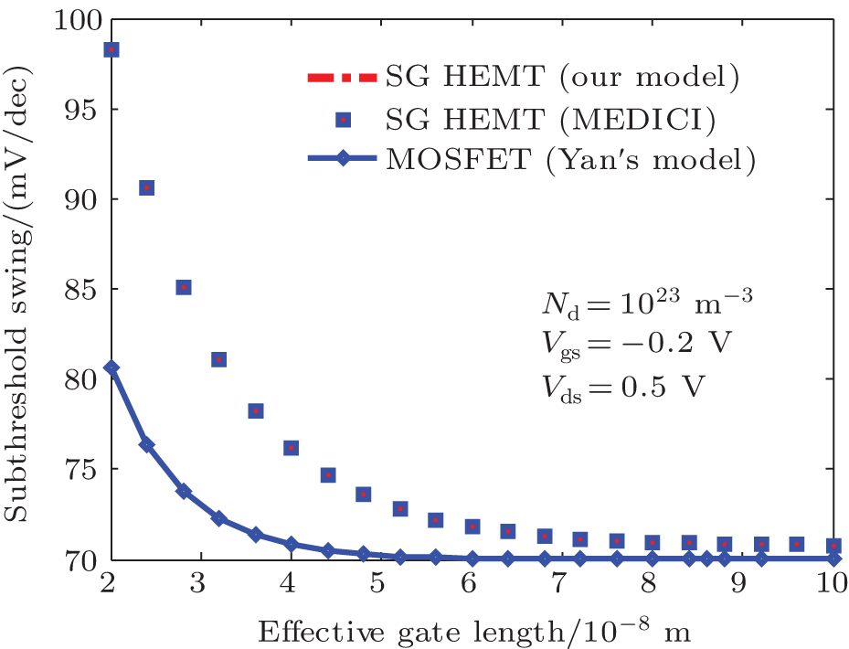 | Fig. 4. Dependence of the subthreshold swing on the effective gate length, the analytical results are compared with simulation results and MOSFET results. |
Figure 5 shows the channel length versus the threshold voltage roll-off for various values of the AlInSb layer thickness, i.e., d = 20 nm, 25 nm, 30 nm. As the channel length increases, the threshold voltage also increases. For d = 30 nm, the threshold voltage roll-off is at minimum. It is obvious that due to the small threshold voltage roll-off, the proposed model can be used in designing the single gate HEMT for small devices.
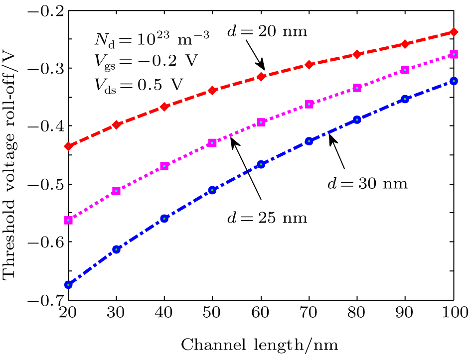 | Fig. 5. Variation of the threshold voltage roll-off with the channel length for various values of AlInSb layer thickness. |
The scaling theory for single gate AlInSb/InSb HEMTs is derived by considering the effective conducting path effect. The potential in the effective conducting path is developed. A simple scaling equation is developed, and by solving this equation, the minimum channel potential Φ deff, min and the new scaling factor α are obtained to model the subthreshold behavior of the HEMTs. The obtained analytical results are compared and verified against TCAD simulation results. The developed model analyzes the subthreshold conduction in the HEMT, which corresponds to the leakage current. Our model improves the performance of the device by minimizing the leakage current. The subthreshold swing is enhanced for higher scaling factors. The threshold voltage roll-off is also minimal, which greatly eliminates the DIBL effects.
| 1 |
|
| 2 |
|
| 3 |
|
| 4 |
|
| 5 |
|
| 6 |
|
| 7 |
|
| 8 |
|
| 9 |
|
| 10 |
|
| 11 |
|
| 12 |
|
| 13 |
|
| 14 |
|
| 15 |
|
| 16 |
|
| 17 |
|
| 18 |
|
| 19 |
|