Electric field effect in ultrathin zigzag graphene nanoribbons
[Zhang Wen-Xing† , Liu Yun-Xiao‡, Tian Hua, Xu Jun-Wei, Feng Lin]
, Liu Yun-Xiao‡, Tian Hua, Xu Jun-Wei, Feng Lin]
|
|


†Corresponding author. E-mail: zhangwenxing@tyut.edu.cn
‡Corresponding author. E-mail: liuyunxiao0917@link.tyut.edu.cn
*Project supported by the National Natural Science Foundation of China (Grant Nos. 11204201 and 11147142) and the Natural Science Foundation for Young Scientists of Shanxi Province, China (Grant No. 2013021010-1).
The electric field effect in ultrathin zigzag graphene nanoribbons containing only three or four zigzag carbon chains is studied by first-principles calculations, and the change of conducting mechanism is observed with increasing in-plane electric field perpendicular to the ribbon. Wider zigzag graphene nanoribbons have been predicted to be spin-splitted for both valence band maximum (VBM) and conduction band minimum (CBM) with an applied electric field and become half-metal due to the vanishing band gap of one spin with increasing applied field. The change of VBM for the ultrathin zigzag graphene nanoribbons is similar to that for the wider ones when an electric field is applied. However, in the ultrathin zigzag graphene nanoribbons, there are two kinds of CBMs, one is spin-degenerate and the other is spin-splitted, and both are tunable by the electric field. Moreover, the two CBMs are spatially separated in momentum space. The conducting mechanism changes from spin-degenerate CBM to spin-splitted CBM with increasing applied electric field. Our results are confirmed by density functional calculations with both LDA and GGA functionals, in which the LDA always underestimates the band gap while the GGA normally produces a bigger band gap than the LDA.
Spintronics is a possible technology to conquer the bottleneck in electronic industry where the quantum effect becomes remarkable with the size of devices decreasing to nanometers.[1– 6] Besides the half-metal materials, [2, 3, 7] spin-selective semiconductors[8– 10] are also natural candidates for spintronics. A few kinds of low-dimensional materials are proposed to be spin-selective under applied electric fields, including graphene nanoribbons, [11– 17] silicene nanoribbons, [18– 20] germanene nanoribbons, [21, 22] and so on. The zigzag graphene nanoribbon (ZGNR) is a one-dimensional planar form of carbon, and it is stable with dangling bonds being saturated by hydrogen atoms or other chemical groups like methyl group, fluorine atom, and so on.[23– 26] The spin texture of ZGNR can be tuned by structural modification on the ribbon edges, such as sawtooth zigzag edges, [27– 29] substitution of carbon atoms, [30, 31] and Stone– Wales defects.[32, 33] The spin properties of ZGNR wider than four zigzag chains (> 4ZGNR) have been studied a lot. However, the spin texture and electric field effect remain unknown for ultrathin ZGNR with only three or four carbon chains (3ZGNR, 4ZGNR) as shown in Fig. 1. We reveal the coexistence of a normal spin-degenerate conducting mechanism and spin-selective conducting mechanism in such ultrathin ZGNRs by applying an in-plane electric field perpendicular to the direction of the ribbon edge.
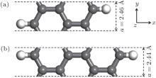
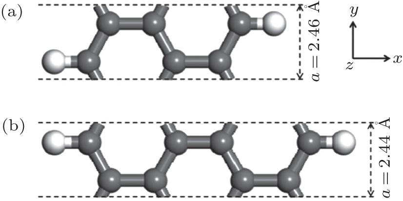 | Fig. 1. Optimized atomic structures of (a) 3ZGNR and (b) 4ZGNR. One unit cell is shown between two parallel slashed lines, and the lattice constant is a. The applied electric field is along the x axis. Black balls are carbon and white ones are hydrogen. |
Our first-principles calculations are carried out with the CASTEP package based on the local density approximation (LDA) of CA-PZ[34] functional using a norm-conserving peseudopotential.[35] Self-consistent results are obtained with a plane-wave cutoff of 680 eV on a 1× 50× 1 Monkhorst– Pack k-point grid. A supercell with a vacuum layer of 15 Å is used to ensure decoupling between neighboring slabs. For structural relaxation, all atoms are allowed to relax until the atomic forces are smaller than 0.005 eV/Å . The electric field E is applied along the positive direction of the x axis as shown in Fig. 1.
Figure 1 illustrates the atomic structures of 3ZGNR and 4ZGNR. The experimental lattice constant of graphene (2.45 Å ) is used for the initial geometries. Hydrogen atoms are used to saturate the dangling bonds of the carbon atoms on the edges. Both geometries of 3ZGNR and 4ZGNR are fully optimized. After the optimization, the lattice constant increases a little (∼ 0.4%) for 3ZGNR due to the odd number of carbon chains and decreases a little (∼ 0.3%) for 4ZGNR due to the even number of carbon chains. Both structures remain planar.
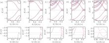
The critical spin-polarized band structures of 3ZGNR are shown in Fig. 2 with increasing E from 0 V/Å to 0.500 V/Å by a step of 0.005 V/Å . The Fermi level (EF) is not set to zero. For 0 V/Å , the conduction band minimum (CBM) and the valence band maximum (VBM) are spin-degenerate. Without the applied field, there is only one conduction band minimum, which locates around the X point (CBMX, KX = π /a) in the one-dimensional wavevector space. As we already know, the CBMX for wider ZGNRs is split in energy with respect to two spins α and β 


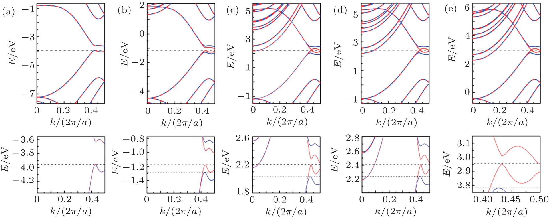 | Fig. 2. Band structures of 3ZGNR under increasing applied fields. Bottom panels are enlarged views of the upper panels around EF. For spins, α and β are displayed in red and blue, respectively. Five electric fields of (a) 0 V/Å , (b) 0.200 V/Å , (c) 0.445 V/Å , (d) 0.460 V/Å , and (e) 0.500V/Å are applied to the system respectively. |
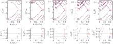
The spin-polarized band structures of 4ZGNR are shown in Fig. 3 with increasing E from 0 V/Å to 0.500 V/Å by a step of 0.005 V/Å . The EF is not set to zero either. As shown in Fig. 3(b), when the electric field is applied, the CBMX and VBMX of 4ZGNR are spin-splitted, while the conduction bands go down in the vicinity of both Γ and X points, that is, the band structure of 4ZGNR follows the same tendency of 3ZGNR. However, when E is increased to 0.380 V/Å (Fig. 3(c)), the normal minimum 
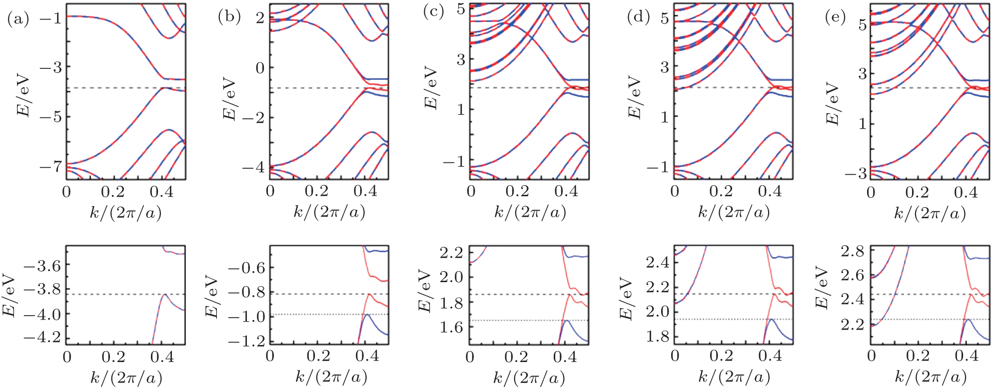 | Fig. 3. Band structures of 4ZGNR under increasing applied fields. Bottom panels are enlarged views of the upper panels around EF. For spins, α and β are displayed in red and blue, respectively. Five electric fields of (a) 0 V/Å , (b) 0.200 V/Å , (c) 0.380 V/Å , (d) 0.400 V/Å , and (e) 0.420 V/Å are applied. |
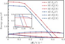
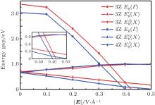
Figure 4 illustrates the relationship between the strength of the electric field E and the spin-splitted energy gap of 3ZGNR and 4ZGNR at different k points, Eg (Γ ), 
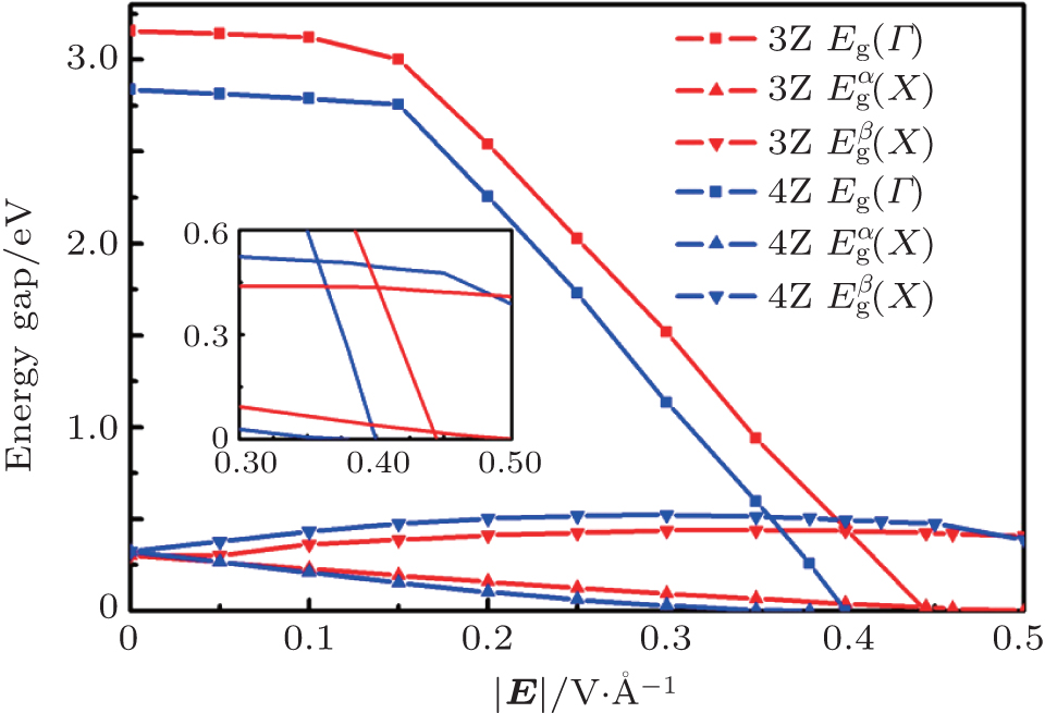 | Fig. 4. Dependence of band gap on the strength of electric field (E) for 3ZGNR (red) and 4ZGNR (blue). The band gap is obtained by LDA calculation. |
Besides the common X point conduction, both 3ZGNR and 4ZGNR have Γ point conduction. This is a feature of the ultrathin ZGNRs different from wider ZGNRs, and there is a distinction between 3ZGNR and 4ZGNR. In 3ZGNR as shown in Fig. 4, the E for closing Eg (Γ ) (0.445 V/Å ) is lower than that for closing
The different effects of the electric field between ultrathin and wider ZGNRs originate from the different ribbon widths. It is well known that the localized edge states are ferromagnetic in ZGNRs. The main difference of conducting mechanism between ultrathin ZGNRs and wide ZGNRs is caused by the different distances between the two edges, i.e., the width of the ribbon, and the corresponding interactions between opposite edge states in the narrow ZGNRs.[2, 3] In nanoribbons, EF locates close to the X point in momentum space under zero bias, and the electrons in the vicinity of EF locate around the two edges in real space, which contribute to the X point conduction. On the other hand, electrons at the Γ point are distributed across the entire nanoribbon in real space. Thus, the influence of the electric field on the electronic structure depends on the side to surface ratio. For ultrathin nanoribbons, the two edges almost occupy the whole area of the ribbon and the electrons redistribute obviously for both X and Γ points, thus the influence of the electric field is strong for both conducting mechanisms. For wider nanoribbons, only the electrons moving along the edges redistribute obviously, while the electrons at the Γ point are weakly affected because most of them are inside the ribbon. The distributing distance of the localized edge states determines the critical width of ZGNRs. From systematic calculations, we find that 4ZGNR is the critical width. The change of conducting mechanism disappears for ZGNRs wider than 4 carbon chains, and all wide ZGNRs only have one kind of conducting mechanism which is spin-splitted around the X point. In applications, the collaboration and competition between the two conducting mechanisms should be considered, which can be checked and verified by studying the density of states around EF using spin-polarized scanning tunnelling microscopy (STM) and scanning tunnelling spectroscopy (STS). In addition, only electrons with one kind of spin can be conductive in the X point conduction, while both α and β electrons can be conductive in the Γ point conduction, when the applied electric field increases. This property makes new electronic devices, which are able to work in both conventional (spin-degenerate) or spin-polarized modes, possible.
The conducting mechanism may change due to the underestimation of the band gap in LDA calculations. To check the effect of underestimation, both 3ZGNR and 4ZGNR are also studied with the generalized gradient approximation (GGA) based on PBE functional[38] under the same precision as the LDA calculations. As we know, the GGA functional always gives a wider band gap than the LDA. The results of GGA are shown in Fig. 5. For 3ZGNR, the results of LDA and GGA are qualitatively the same. For 4ZGNR, the results of LDA and GGA show inverse order of transition between two conducting mechanisms with increasing electric field; it is due to the different deviation in estimation of the band gap in LDA and GGA. The electric fields needed to close the gap between the VBMX and the spin-degenerate CBMΓ are analogous for LDA and GGA calculations. Moreover, a much higher electric field is needed to close the gap between the VBMX and the spin-splitted CBMX in GGA due to the remarkable band gap around the X point.
 | Fig. 5. Dependence of band gap on the strength of electric field (E) for 3ZGNR (red) and 4ZGNR (blue). The band gap is obtained by the GGA calculation. |
The electric field effect in ultrathin ZGNRs (3ZGNR, 4ZGNR) is studied with density functional theory. New conducting channels are open with increasing applied field. Both Γ point conduction and X point conduction should be considered in applications of ultrathin ZGNRs, which is different from that of the wide ones. The phenomena result from the quantum confinement effect and make new electronic devices working in both conventional or spin-polarized modes possible.
| 1 |
|
| 2 |
|
| 3 |
|
| 4 |
|
| 5 |
|
| 6 |
|
| 7 |
|
| 8 |
|
| 9 |
|
| 10 |
|
| 11 |
|
| 12 |
|
| 13 |
|
| 14 |
|
| 15 |
|
| 16 |
|
| 17 |
|
| 18 |
|
| 19 |
|
| 20 |
|
| 21 |
|
| 22 |
|
| 23 |
|
| 24 |
|
| 25 |
|
| 26 |
|
| 27 |
|
| 28 |
|
| 29 |
|
| 30 |
|
| 31 |
|
| 32 |
|
| 33 |
|
| 34 |
|
| 35 |
|
| 36 |
|
| 37 |
|
| 38 |
|