Progress and prospects of GaN-based LEDs using nanostructures

Progress and prospects of GaN-based LEDs using nanostructures |
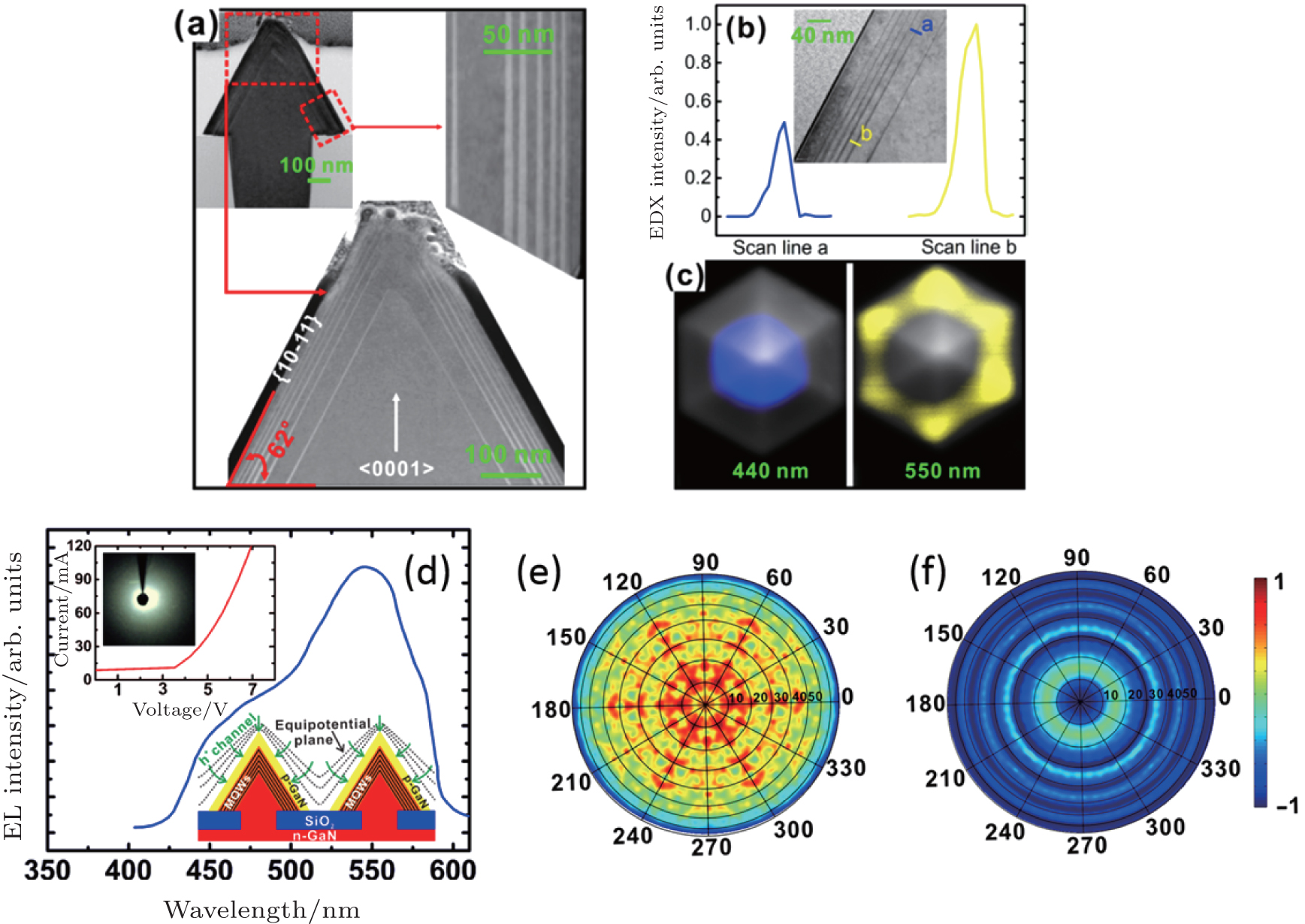
| (a) TEM cross-section of a single nano-pyramid white LED. (b) For the cross-section cut along the ridges, the normalized TEM-EDX line scan analysis was carried out perpendicular to the QW, as indicated in the lines a (blue) and b (yellow), representing the middle position of the upper part and the lower part of the nanopyramid, respectively. (c) Monochromatic CL images at the given wavelength as on the images. (d) EL emission spectra of the LEDs. The inset shows the current–voltage ( I – V ) characteristic and photography of light emission for the LEDs. (e) Far-field distribution of light energy for the nanopyramid white LED and (f) the flat-top LED. |
 |