Zhao Li-Xia†, Yu Zhi-Guo, Sun Bo, Zhu Shi-Chao, An Ping-Bo, Yang Chao, Liu Lei, Wang Jun-Xi, Li Jin-Min. Progress and prospects of GaN-based LEDs using nanostructures* . Chinese Physics B, 2015, 24(6): 068506
Permissions
Progress and prospects of GaN-based LEDs using nanostructures*
Zhao Li-Xia†, Yu Zhi-Guo, Sun Bo, Zhu Shi-Chao, An Ping-Bo, Yang Chao, Liu Lei, Wang Jun-Xi, Li Jin-Min
Semiconductor Lighting Research and Development Center, Institute of Semiconductors, Chinese Academy of Sciences, Beijing 100083, China
*Project supported by the National Natural Science Foundation of China (Grant No. 61334009), the National High Technology Research and Development Program of China (Grant Nos. 2015AA03A101 and 2014BAK02B08), China International Science and Technology Cooperation Program (Grant No. 2014DFG62280), the “Import Outstanding Technical Talent Plan” and “Youth Innovation Promotion Association Program” of the Chinese Academy of Sciences.
Abstract
Progress with GaN-based light emitting diodes (LEDs) that incorporate nanostructures is reviewed, especially the recent achievements in our research group. Nano-patterned sapphire substrates have been used to grow an AlN template layer for deep-ultraviolet (DUV) LEDs. One efficient surface nano-texturing technology, hemisphere-cones-hybrid nanostructures, was employed to enhance the extraction efficiency of InGaN flip-chip LEDs. Hexagonal nanopyramid GaN-based LEDs have been fabricated and show electrically driven color modification and phosphor-free white light emission because of the linearly increased quantum well width and indium incorporation from the shell to the core. Based on the nanostructures, we have also fabricated surface plasmon-enhanced nanoporous GaN-based green LEDs using AAO membrane as a mask. Benefitting from the strong lateral SP coupling as well as good electrical protection by a passivation layer, the EL intensity of an SP-enhanced nanoporous LED was significantly enhanced by 380%. Furthermore, nanostructures have been used for the growth of GaN LEDs on amorphous substrates, the fabrication of stretchable LEDs, and for increasing the 3-dB modulation bandwidth for visible light communication.
Gallium nitride (GaN) is an extremely promising direct wide bandgap semiconductor material for optoelectronics, [1] and it has been developed significantly during the past 20 years. In the early 1990s, after the achievement of high quality GaN growth using an AlN or GaN nucleation layer[2, 3] and p-type conductivity, [3] Nakamura et al. developed the GaN-based blue LED with quantum well structure[4, 5] and successfully fabricated the first white LED.[6] Since then, numerous researchers started to pay attention to III-nitride-based LEDs because of their advantages in the applications of full-color display, solid state lighting, etc. The luminous efficacy increased continuously, which boosted the revolution in illumination and other cutting edge applications. Recently, with the demonstration of 303 lm/W, another significant LED milestone was announced for high power white LEDs by Cree. Ltd.[7] In the same year, the Nobel Prize for physics was awarded to Isamu Akasaki, Hiroshi Amano, and Shuji Nakamura for their invention of efficient blue light-emitting diodes, which have enabled bright and energy-saving white light sources.[8]
The external quantum efficiency of LEDs is given by a product of the internal quantum efficiency (IQE) and the light extraction efficiency (LEE). The internal quantum efficiency is determined by crystal quality and epitaxial layer structure. Although the native substrates are available for nitrides, due to the limited availability and relatively high cost of sufficiently large single GaN crystals for use as substrates, most GaN-based LEDs are grown on foreign substrates, such as sapphire and SiC. During the last two decades, lots of technology, including nanostructures, has been focused on improving the material growth and device fabrication to enhance the internal quantum efficiency as well as the extraction efficiency.
In this paper, we provide an overview of the current application of nanostructures in the GaN-based LED, including: 1) the nanostructures to improve the crystal quality and, in so doing, enhance the internal quantum efficiency; 2) the nanostructures to modify the surface/interface morphology to decrease the internal reflection and increase the extraction efficiency; 3) one-dimensional nanostructures; and 4) surface plasmon LEDs. At last, we will attempt to highlight the perspective of nanostructures beyond illumination, especially for cutting edge applications.
2. Application of nanostructures to III-nitride LEDs
2.1. Nanostructures to improve internal quantum efficiency
The large lattice constant mismatch (15%) between sapphire and GaN leads to a high dislocation density (1010 cm− 2) in the GaN epitaxial film. These high defect densities can reduce charge carrier mobility, minority carrier lifetime, and thermal conductivity, and hence, degrade device performance. Implementation of epitaxial lateral overgrowth (ELOG) significantly decreases the dislocation density to 107 cm− 2.[9] With ELOG technology, parts of the highly dislocated GaN are masked with a dielectric mask and the threading dislocations are prevented from propagating into the over-layer. Hence, GaN layers grown above the opening keep the same threading dislocation density as the template, at least during the early stages of growth. In addition, coalescence boundaries are formed due to mis-registry between two laterally growing fronts, and voids are normally formed above the mask. Tilting and dislocations are also generated among the coalescence regions. Although this technique improves the crystal quality of the overgrown layer, it inherently suffers from inevitable growth interruption, in which an SiO2 or SiNx mask must be deposited after a 1-μ m– 2-μ m thick GaN layer growth.[10, 11] This two-step metal– organic chemical vapor deposition (MOCVD) growth process is complicated and time consuming, and not suitable for commercial application. Moreover, mask-related drawbacks also induce possible impurity contamination and strain in the subsequently grown layers.
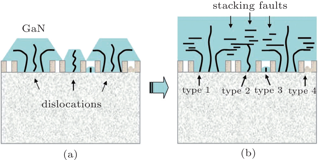
In order to overcome the problems induced by ELOG, patterned sapphire substrates (PSS) technology without mask, and with no suspension during growth, have been widely proposed afterwards.[12] Using PSSs may not reduce the dislocation density to the magnitude that ELOG can achieve, but there is no contamination from the dielectric mask, and the growth process can be simplified to one step, which is suitable for mass production. In addition, the external efficiency can be enhanced based on the effect of optical reflection from the side edge of the etched sapphire substrate. Many kinds of patterns have been formed, such as lens-shaped, hemispherical, grooved, volcano-shaped, cone-shaped, by methods of photolithography, electron beam lithography (EBL), laser treatment, etc. If the pattern size is nanoscale, the LEDs grown on nano-patterned sapphire substrate (NPSS) provide better LEE more efficiently because NPSS has a much higher density of patterns, which can increase the chance of light scattering. The highly ordered nanoscale patterns in a PSS may induce the photonic crystal effect as well, which can further enhance the LEE.[13] In addition, the dislocation density that develops during overgrowth will be lower. Figure 1 shows schematics of the overgrowth process, the formation of dislocations, stacking faults, and voids at the initial stage of epitaxy, as well as the potential mechanisms for minimization of threading dislocations.[14]
Fig. 1. Schematics of (a) the overgrowth process and the formation of dislocations, stacking faults, and voids at the initial stage of epitaxy, and (b) four mechanisms that might account for the reduction of the TDD.[14]
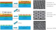
Especially for the deep UV LEDs, the coalescence of an AlN buffer layer upon PSS needs to be 10 μ m, which significantly increases the growth time and cost. To achieve high light output power along with a thinner coalescence thickness, NPSS has been used for nanoscale ELO of an AlN template layer in our group to fabricate DUV LEDs.[15, 16] Figure 2 shows the process flow chart for nano-patterned sapphire substrates and the corresponding SEM images.
Fig. 2. The process flow chart for nano-patterned sapphire substrates, and the corresponding SEM images.
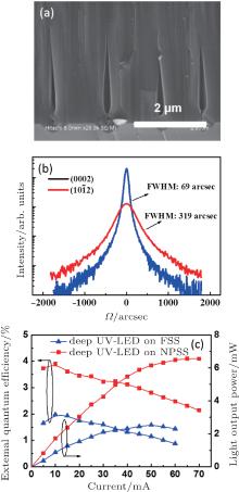
With NPSS, the coalescence thickness of AlN film can be as little as 3 μ m, as shown in Fig. 3(a). The full width at half-maximum (FWHM) values of (002) and (102) reflections are 69 arcsec and 319 arcsec, respectively, as shown in Fig. 3(b). The corresponding screw and edge dislocation densities are calculated to be 1.0× 107 cm2 and 1.2× 109 cm2. This indicates that the AlN material quality is much better than AlN grown on flat sapphire substrate, which has (002) and (102) XRCs of 126-arcsec and 573-arcsec FWHMs. An enhancement of IQE by 43% was measured by temperature-dependent photoluminescence. The 282-nm DUV-LED fabricated on this AlN/NPSS template has reached light-optput power (LOP) of 3.03 mW and external quantum efficiency (EQE) of 3.45% at current 20 mA, which is 98% higher than that achieved on the conventional AlN/FSS template, as shown in Fig. 3(c).
Fig. 3. (a) A cross-sectional SEM image of AlN grown on NPSS. (b) X-ray rocking curves of (002) and (102) diffractions for the AlN films grown on the NPSS. (c) LOP– I– EQE curves of the deep-UV LEDs grown on NPSS and FSS.
2.2. Nanostructures to improve light extraction efficiency
Following rapid development in material growth methods, such high values of internal quantum efficiency have been obtained that little room is left for further improvement. In order to further enhance the luminous efficacy, researchers have paid lots of attention to enhance the extraction efficiency. As for the GaN-based LEDs, considering the large difference of refractive index between GaN (n = 2.5) and the air interface, the critical angle for the light escape cone is only about 23° . Most of the light generated in the LED will be trapped by total internal reflection and cannot be extracted to the outside. Common techniques of boosting light extraction from an LED chip include geometrical chip shaping; [17] surface/interface morphology modification on n-GaN, [18] p-GaN[19] or ITO transparent conductive layer; [21– 23] microlens array; [20] integration of photonic crystal (PhC) structure; [24– 34] etc.
2.2.1. Surface roughening
In 2004, Fujii et al.[18] reported a roughened surface of n-side-up GaN-based LEDs using photo-electro-chemical (PEC) etching. The output power of an optimally roughened surface LED is two to threefold better than that of an LED without surface roughening. In 2005, Huang et al.[19] developed an InGaN/GaN LED with a nano-roughened top p-GaN surface using an Ni nano-mask and laser etching. The light output of the InGaN/GaN LED with a nano-roughened top p-GaN surface is 1.55 times that of the conventional LED. However, the disadvantage of this surface roughening approach is the difficulty in controlling the process. Furthermore, the plasma etching of the top p-GaN contacting layer will lead to damage and significantly degrade electrical and optical properties of the device due to increased Ohmic contact resistance and leakage currents.
Instead, using an SiO2/polystyrene (PS) microlens array on the top surface of the LEDs has been reported[20] to significantly increase the external quantum efficiency of the devices by 219%. The refractive indices of PS and SiO2 microspheres are 1.58 and 1.46, respectively. The use of these arrays allows the photons emanating from the quantum well (QW) to scatter out from the LEDs structure with a larger “ effective” photon escape cone and reduction of the Fresnel reflection. In addition, surface roughening or patterning of the indium tin oxide (ITO) current spreading layer have been demonstrated as an alternative method for improving light extraction efficiency without degrading electrical properties.[21– 23] Besides that, owing to the increasing demand for raw materials, especially indium, scientists also search for alternatives to indium tin oxide, such as carbon nanotubes, graphene, metal nanowire networks as transparent conductive electrodes. Details can be found in Ref. [35].
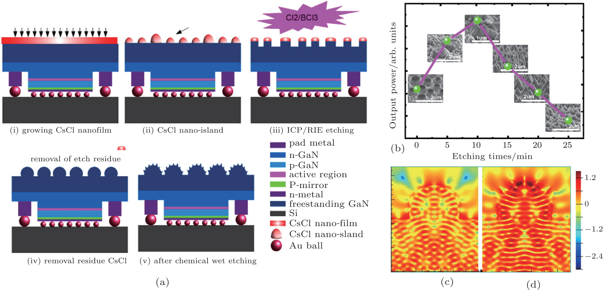
In addition, the extraction efficiency of LEDs has been reported to be determined by the nano-cone density[36] of the surface. LEDs with an integrated textured surface can increase the angular randomization of photons at the emission surface and result in a large enhancement of light output power.[37, 38] We have also fabricated InGaN flip-chip light-emitting diodes with hemisphere-cones-hybrid combined nanostructures. The light output power shows an enhancement factor of 1.9 at 350-mA injection current.[39] Figure 4 shows schematic diagrams of the fabrication process [(i)– (v)] for nano-textured flip-chip LEDs. The finite-difference time-domain (FDTD) simulation shows that the distinct light scattering behavior of the integrated surface is due to the combination of diffraction of waves at the nano-cones edges and complicated interference of waves within the hemispheres and nano-cones, as shown in Figs. 4(c) and 4(d).
Fig. 4. (a) Schematic diagrams of fabrication process for nanotextured flip-chip LEDs. (b) Light-output power of the nanotextured flip-chip LEDs as a function of chemical etching times, with the corresponding SEM images of nanotextured n-GaN surface shown in the background. (c) FDTD simulation results of wave propagating through an individual hemisphere surface feature and (d) an individual hemisphere-cones-hybrid surface feature.
2.2.2. Photonic crystals
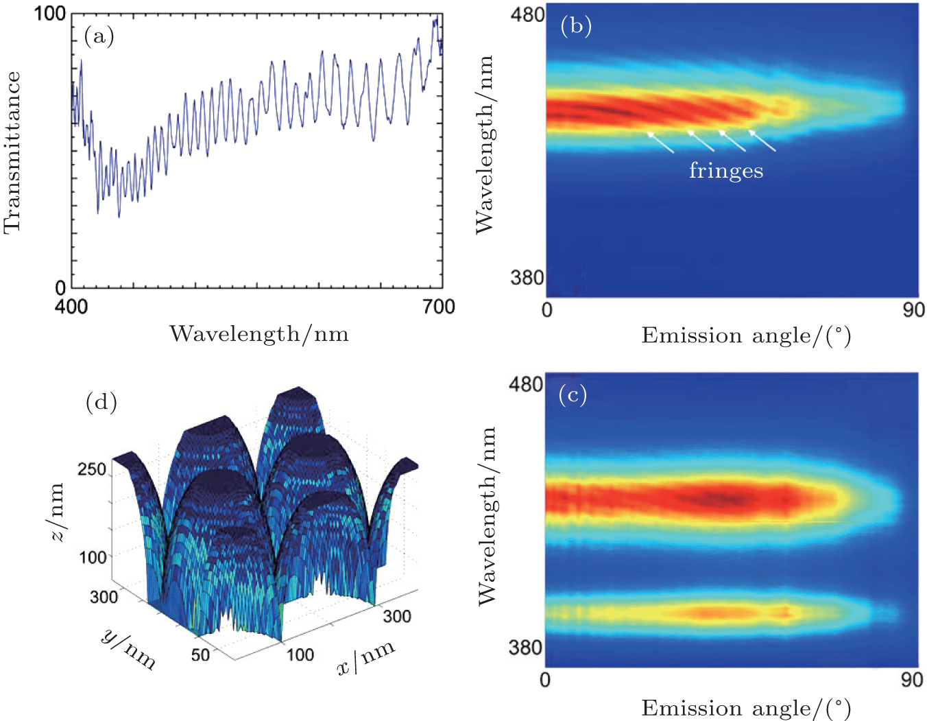
Photonic crystals are dielectric perturbations on the nano-scale intended to control the way of light propagation in the medium. The integration of photonic crystal within LEDs can also provide a solution to enhance the light extraction.[24] Fujita et al.[25] demonstrated the simultaneous inhibition and redistribution of spontaneous light emission in photonic crystal. Fu et al.[26] demonstrated the existence of a photonic band gap from the PhC structure, as shown in Fig. 5. The enhancement of the light extraction is due to strengthening of coupling modes by the diffractive nature of light emission from the PhC structure. A transmission dip was identified, and a threefold enhancement in light extraction was achieved, as determined from the measured angular photoluminescence emission pattern, which is correlated well with the results simulated by the FDTD method.
Fig. 5. (a) Measured transmission spectrum, with reference to a GaN LED as-grown sample; Measured and normalized angle-resolved PL spectrum for (b) as-grown sample and (c) PBG structure; (d) Results of FDTD simulation, showing energy flux distribution across the HE array structure.[26]
In 2009, Wierer et al.[27] reported the III-nitride photonic crystal LEDs with high light extraction of 73% emitting at 450 nm, a significant step forward in high-performance LEDs for solid-state lighting applications. However, the photonic crystal structure is normally fabricated by electron beam lithography, [28– 34] nano-imprint lithography[40– 47] or holographic lithography.[48, 49] These methods are costly and complex to operate.
Considering mass production and cost, nanosphere lithography (NSL)[50– 54] has been proposed as an efficient technique to form the PhC nanostructures and increase the extraction efficiency of GaN-based LEDs by our group.[55– 58] The nanosphere array can be simply coated by spin-coating or vertical deposition, producing two-dimensional close-packed hexagonal monolayer. Afterwards, the self-assembled sphere array can serve as an etch mask for pattern transferring to form periodic arrays with air-holes or pillars. Recently, with multiple-exposure, a more pronounced enhancement has been demonstrated.[59]
Aside from the increase of light emission, photonic crystals can also be used to design emission at a particular angle. For example, for non-polar GaN-based LEDs incorporated with the PhCs, due to the combined effect of the polarization-preserving and directional extraction properties of the photonic-crystals, polarized light has been demonstrated with higher brightness.[60] This will be desirable for LCD displays and polarized back-light sources in high efficiency TV displays and cell phones. There are also some other nanostructures to enhance light extraction efficiency; the details can be found in the review article.[61]
2.3. Nanorod LEDs
The work on GaN and InGaN one-dimensional (1D) nano-materials was initiated in the late 1990s.[62– 64] In 2004, high-brightness and high-efficiency light-emitting diodes with dislocation-free InGaN/GaN multiple quantum well (MQW) nanorod arrays (NRAs) grown by MO-HVPE were demonstrated.[65] Compared to conventional planar LED heterostructures, the use of 1D nanorods offers several extraordinary advantages, such as reduced dislocation densities, [66, 67] polarization fields, [68] and enhanced light output efficiency due to the large surface-to-volume ratios, as well as compatibility with low cost, large-area Si substrates.[69] Furthermore, it was demonstrated that multicolor emission can also be achieved by varying nanorod diameters, composition and morphologies or external electrical field.[70– 72] In addition, the defect-free nanowires also significantly reduce the Auger recombination and droop effect.[73, 74]
GaN-based nanorod LEDs can be fabricated by either top-down or bottom-up approaches. The fabrication of GaN-based LED using a top-down method[68, 75] is normally formed by dry etching, but top-down etching-induced sidewall damage will create a large amount of defects and leakage currents that limit the light output power. Therefore, a passivation process should commonly be considered. Chiu et al.[75] reported the fabrication of InGaN/GaN nanorod LEDs using inductively coupled plasma reactive-ion etching (ICP/RIE) via self-assembled Ni nanomasks followed by a photo-enhanced chemical (PEC) wet oxidation process. The electroluminescence spectrum shows more efficiency and a 10.5-nm blue-shifted peak with respect to the as-grown LED sample, indicating a strain relaxation effect. Huang’ s group[68] demonstrated the InGaN/GaN MQW light-emitting diodes with a self-organized nanorod structure. The nanorod array was realized by lithography of surface patterned silica spheres followed by dry etching. A layer of spin-on glass (SOG) was used for the purpose of the electric isolation of each of the parallel nanorod LED units. Both the EL and Raman spectroscopy showed a strain relaxation of the nanostructures.
Bottom-up fabrication is another alternative method for nanorod LEDs. Many kinds of growth methods are used for the growth of nitride 1D nanorod arrays, including hydride vapor phase epitaxy (HVPE), molecular beam epitaxy (MBE) and MOCVD. Kim et al.[65] reported MO-HVPE grown high-brightness and high-efficiency LEDs with dislocation-free InGaN/GaN MQW nanorod arrays. Nanorod arrays on sapphire substrate were buried in spin-on glass (SOG) to isolate the individual nanorods and bring p-type nanorods in contact with p-type electrodes, as shown in Fig. 6. Due to the absence of dislocations and the large surface areas provided by the sidewalls of nanorods, both internal and extraction efficiencies were significantly enhanced. At 20-mA current, the MQW nanorod array LEDs emit about 4.3 times more light than conventional LEDs, even though overall active volume of the MQW nanorod array LEDs is much smaller than that of conventional LEDs.
Fig. 6. Schematic diagram and SEM image of cross-sectional MQW NRA LED structures and electroluminescence (EL) characteristics of InGaN/GaN MQW NRAs LEDs.[65]
However, as the principal technique for the growth of III-nitride films and devices, MOCVD offers the advantages to open possible compatibility with thin film technology and scale up to wafer scale production. In 2003, gallium nitride nanowires were first synthesized via MOCVD with catalyst, [76] but as for the device application, a problem with catalytic processes is that the metal catalyst will inevitably incorporate into the nanowire, which may be prohibitive for device applications. In order to solve this problem, vertically aligned and faceted GaN nanorods with controlled diameter were grown without a catalyst by Deb et al.[77] and Hersee et al., [78] respectively.
In the bottom-up method employing MOCVD, core/shell nanostructures are usually obtained. Qian et al.[79] fabricated core/multishell nanowire LEDs with an n-GaN core and InxGa1− xN/GaN/p-AlGaN/p-GaN shells in 2005. Electroluminescence measurements demonstrated that in forward bias the core/multishell nanowires function as light-emitting diodes, with tunable emission from 365 nm to 600 nm and high quantum efficiencies. Afterward, they demonstrated the laser behavior of individual MQW nanowire structures by optical excitation with In composition-dependent emission from 365 nm to 494 nm.[80] Besides the composition, the color of the core/shell GaN-based LEDs can also be simply controlled in the full visible-color range from red to blue by adjusting the forward bias.
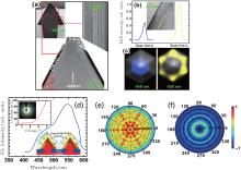
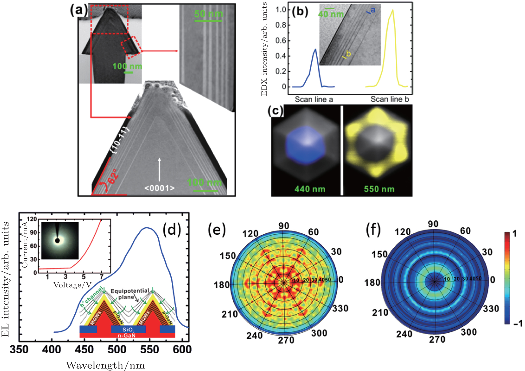
Hexagonal nanopyramid is a core/shell nanostructure, which can be formed during bottom-up growth. The advantage of this low-dimensional structure, with semi- and non-polar facets, is to enhance internal quantum efficiency. Our research group[81] has fabricated highly ordered hexagonal nanopyramid light emitting diodes with InGaN/GaN quantum wells grown on nano-facets, demonstrating an electrically driven phosphor-free white light emission, as shown in Fig. 7. The results show that both the quantum well width and indium incorporation increased linearly along both the planes toward the substrate and the perpendicular direction to the planes.
Fig. 7. (a) TEM cross-section of a single nano-pyramid white LED. (b) For the cross-section cut along the ridges, the normalized TEM-EDX line scan analysis was carried out perpendicular to the QW, as indicated in the lines a (blue) and b (yellow), representing the middle position of the upper part and the lower part of the nanopyramid, respectively. (c) Monochromatic CL images at the given wavelength as on the images. (d) EL emission spectra of the LEDs. The inset shows the current– voltage (I– V) characteristic and photography of light emission for the LEDs. (e) Far-field distribution of light energy for the nanopyramid white LED and (f) the flat-top LED.
To evaluate the effect of nanopyramid structures on the light extraction of the nanopyramid white LEDs, three-dimensional (3D) FDTD simulations were carried out to numerically predict the light output power and far-field emission patterns, [82] as shown in Figs. 7(e) and 7(f). The conventional LEDs with a flat surface present a far-field pattern with perfect circular symmetry due to the fact that the total internal reflection occurs at the GaN/air interface. Besides, as the light escapes from a very small angle, only a small part of the surface allows light to emit out. The inner and outer radiation ring caused by the Fabry– Perot effect is ascribed to the direct emission from the InGaN MQWs and the reflection from the bottom reflecting boundary, respectively. In contrast, when the nanopyramid structures have been formed at the surface, a radiation pattern with hexagonal symmetry is accompanied by the light spreading over the entire surface, which indicates that the light escape cone is significantly broadened.
Details of the other nanostructure technologies to enhance the extraction efficiency can be found in the review article.[83]
2.4. Surface plasmon LEDs
Plasmon is the quantum of plasma oscillation, and surface plasmons (SP) are confined upon a surface with the bulk plasmon energy as an upper energy limit. Surface plasmon can greatly enhance the photon density of states of the electron– hole pairs and improve the competitiveness of radiative recombination to the non-radiative recombination. Numerous experiments have been conducted to increase the quantum efficiency by surface plasmon– photon coupling.[84– 95] In 2004, Okomoto et al.[84] improved the internal quantum efficiency of the InGaN/GaN quantum well ∼ 7 times using the Ag film to 41%, which created the application of surface plasmon on the GaN-based LEDs. The principle of light emission enhancement using the surface plasmon is that when the electron– hole pairs are close to the surface of metal materials, the coupling between electron– hole pairs and surface plasmon occurs if energy matches. Then the energy of the electron– hole pairs spontaneously emits to the surface plasmon modes, as
where d is the momentum of electron– hole pairs, a is the location of the quantum well related to the metal/semiconductor interface, E(a) is the electric field strength at location “ a, ” and ρ (ħ ω ) is the density of states of the surface plasmon. As the spontaneous recombination rate of the electron– hole pairs is proportional to the density of states of the surface plasmon, which is far greater than that of the dielectric, enhancement of spontaneous recombination rate is expected.
However, some requirements must be met if we want to effectively make use of the surface plasmon for the GaN-based LEDs. First of all, the electron– hole pairs need to be within the near field of the metal area, because the surface plasmon exists just at the surface of the metal materials and decays exponentially with distance. But the thickness of the p-GaN is hundreds of nanometers due to the low hole concentration, which prevents direct coupling between electron– hole pairs in the quantum region and metal materials at the p-GaN surface. Secondly, the electron– hole pairs should be energy-matched to the surface plasmon. In addition, the intrinsic absorption loss of the surface plasmon should be low enough. Thus, the core issue of fabricating the surface plasmon-enhanced GaN-based LED is to put the energy-matched and low-absorption metal materials close to the quantum well region, but without optical– electrical performance degradation. There are three commonly used approaches, which are the thin p-GaN approach, the metal embedded approach, and the top-down approach.
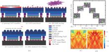
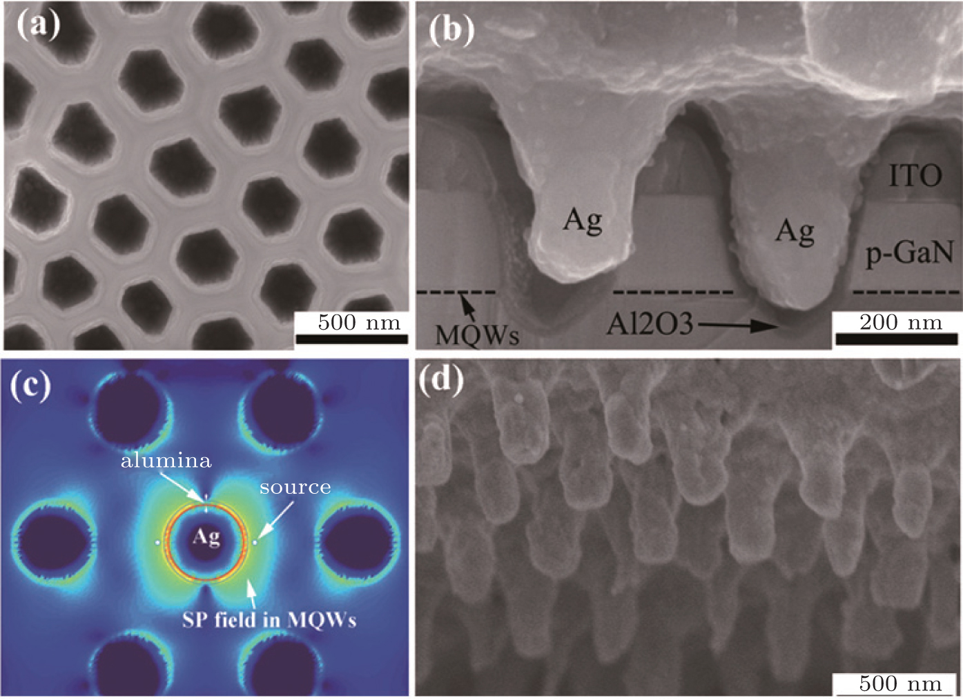
At an earlier stage, the approach with a thin p-GaN layer was proposed.[85– 87] In this case, the thickness of the p-GaN layer was reduced from the conventional 200 nm to 80 nm, and the metal nanoparticles were then deposited on the surface to enable coupling with the quantum well underneath the p-GaN layer. With that approach, the structure of the device is simple, but the hole-injection is still limited by the depletion width of the p-side in the p– n junction, the coupling distance cannot be further reduced. In order to decrease the SP coupling distance, the approach with embedded metal has been used, [88– 92] wherein the metal nanoparticles are embedded above the p-GaN/MQWs or below the n-GaN/MQWs interface. This method can result in an SP coupling distance of 10 nm and a thick enough p-GaN hole-injection layer, but the side effect is that the small size of the metal particles caused by high temperature regrowth leads to a low SP scattering efficiency. In addition, the devices suffer a serious degradation of optical– electrical performance because of both the poor crystal quality of epilayers grown on the metallic layer and the metal diffusion to MQWs at high temperature. Recently, a more flexible SP coupling based on top-down processing technology has been reported.[93– 95] The p-GaN layer with a two-dimensional nano-hole array structure is fabricated using a dry etching mask, followed by metal deposition into the bottom of holes. It is roughly 30 nm– 40 nm above the MQWs for SP coupling. With this method, the metal incorporation is independent of epitaxial growth, which can effectively prevent the quality deterioration of the material caused during the growth. Furthermore, the surface plasmon resonant energy and scattering efficiency of metal particles can be easily manipulated using different mask morphologies. However, the devices have large leakage currents because of the short distance between hole-bottom and MQWs, which not only seriously deteriorates the optical performance, but also limits a further decrease of the distance between the hole-bottom and MQWs. We have overcome the leakage current issue by depositing 15-nm Al2O3 passivation[96] on the pore wall for electrical protection, and then we extended the pore to the quantum well region for the closer coupling. Figure 8 shows SEM images of a nanoporous LED before and after Ag deposition. Furthermore, numerical simulation results show that the SP field of Ag nanorods can laterally penetrate into the MQWs region. In this region, the electron– hole pairs can be strongly coupled with SP, which leads to a great increase of the radiative recombination rate caused by the extremely high density of states of the SP.
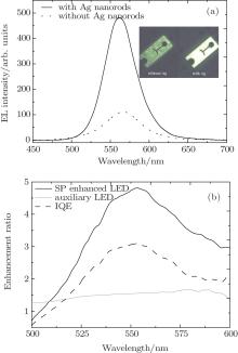
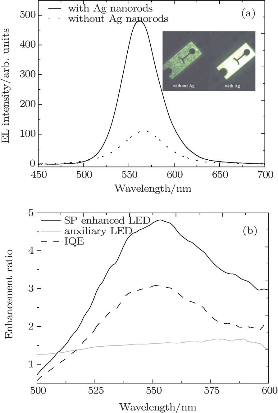
Fig. 8. (a) Top view SEM image of nanoporous LED before Ag deposition. (b) Cross section of nanoporous LED with Ag nanorods. (c) The SP field distribution of Ag nanorods simulated by FDTD. (d) SEM image of the Ag nanorods array separated from nanoporous LED.
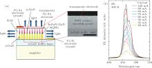
Figure 9(a) shows the EL spectrum of the nanoporous LED with and without Ag nanorods. After filling the Ag nanorods into the nanoporous LED, a 380% enhancement in the EL peak intensity and an obvious blue shift of 5 nm were observed. In order to distinguish the influence of the light extraction from the SP coupling, we also prepared a series of corresponding nanoporous control LEDs, which have the same surface structure of pore morphology, passivation layer thickness, and Ag nanorod morphology as the SP-enhanced nanoporous LED, but a thicker p-GaN layer with 360 nm. In this case, Ag nanorods are located at 100 nm above the MQWs, and no SP coupling would be expected because of the large coupling distance. Figure 9(b) shows the EL enhancement spectrum of the nanoporous control LEDs, which is almost flat with the value of about 1.4 in the range of wavelengths from 500 nm to 600 nm, indicating that no SP coupling was achieved, and this EL intensity enhancement is attributed only to the light extraction enhancement. The EL enhancement spectrum of the SP-enhanced nanoporous LEDs is also shown in Fig. 9(b), which corresponds to the total enhancement factor of SP coupling and light extraction. A peak enhancement factor of 4.8 was observed at 553 nm. Extracting the EL enhancement spectrum of the corresponding control LEDs, the IQE enhancement spectrum of SP-enhanced nanoporous LED can be achieved. A maximum IQE enhancement factor of 3.6 was observed at 550 nm, which is very close to that of the dipole resonance of the silver nanorods. This indicates that the IQE enhancement is attributed to the coupling between SP and MQWs.
Fig. 9. Electroluminescence spectra (a), optical images (inset), and EL enhancement factors (b) of nanoporous LEDs with and without Ag nanorods.
3. Beyond illumination
3.1. Visible light communication
The rapid improvement in the efficiency of solid-state lighting has already stimulated its application for general indoor lighting. However, beyond illumination, GaN-based LED lighting can simultaneously be used for communications, offering the possibility of wireless broadcasting within a room. At the moment, commercial modulation bandwidth of blue GaN-based LEDs is roughly about 20 MHz, which still strongly limits the visible light communication. There are two approaches to increase the modulation speed of an LED. The first one is to increase the carrier concentration in the active region. Increasing the dopant concentration further improves the device speed but introduces too many non-radiative recombination centers, which severely limit the internal efficiency.
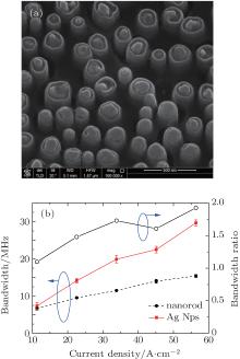
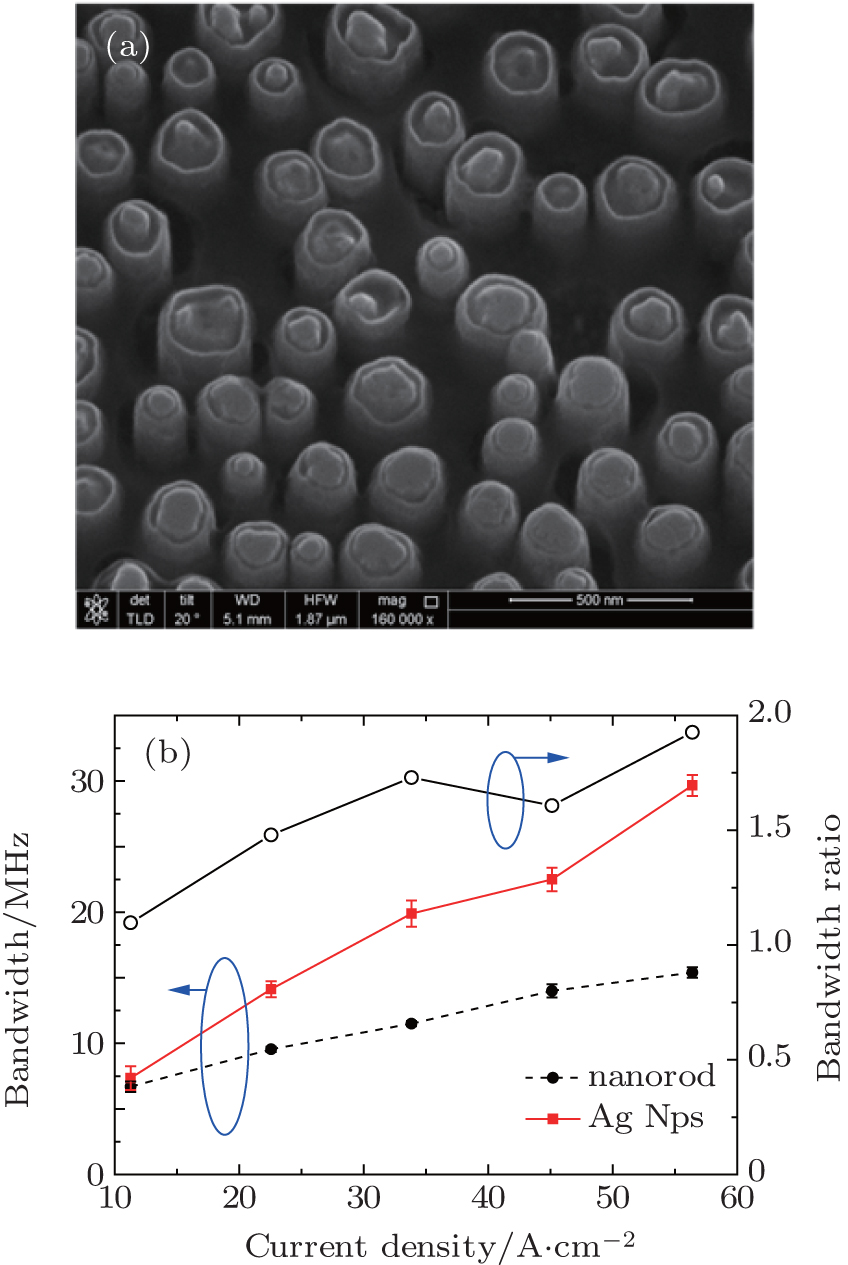
Improving the B constant through the Purcell effect is an effective solution to reach modulation speeds without sacrificing luminous efficacy. It has been reported[97, 98] that localized surface plasmons (LSP) can effectively increase the carrier spontaneous emission rate (the radiative recombination constant B), an effect attributed to the new energy transition channel of electron– hole pairs in LEDs created by the QW-SP coupling. Since the density of states of the SP mode is quite large, the QW-SP coupling rate will be very fast, and thus increase the spontaneous emission rate and decrease the carrier recombination time accordingly. Fluorescence lifetime measurements on emitters of plasmonic nano-antennas reveal enhancements of the spontaneous emission rate even exceeding 1000 times.[99] However, due to the lack of the effective surface plasmon coupling approach, only slight improvements in the spontaneous emission rate of electrical devices were achieved. Since the SP is an evanescent wave that exponentially decays with the distance from the metal surface, nanostructures need be used to modulate the distance of LSP-MQW coupling. Recently, Nami et al. investigated the modulation response of Ag-clad flip-chip GaN/InGaN core-shell nanowire LEDs using FDTD; with the calculated Purcell factor being 57 for the designed structure, the maximum 3-dB modulation bandwidth reached about ∼ 30 GHz.[100] Even so, it is still challenging for fabrication of electrical injected SP-LED to increase the modulation bandwidth. Recently, we also fabricated nanorod LEDs with Ag nanoparticles; The 3-dB modulation bandwidth is enhanced by a factor of 2 at 57 A/cm2 compared with LEDs without surface plasmons, which is mainly due to the SP-MQW effective coupling, as shown in Fig. 10.
Fig. 10. (a) SEM image of the nanorod array covered by the etched SOG. (b) The optical 3-dB bandwidth modulation as a function of injection current density for the nanorod LED without Ag Nps and nanorod LED with Ag Nps.
3.2. Stretchable LEDs
Currently most of the GaN-based LED devices are typically produced on sapphire substrates and the LEDs may be transferred to more thermally conducting, but rigid and planar substrates. The realization of stretchable LEDs will not only permit significantly more durable devices to be fabricated, it will also enable conformal bonding to arbitrary non-planar surfaces and moving parts, which will be useful for applications in robotics, textiles, medical devices, and for integration into electronic-skin applications.
In 2010, transferable gallium nitride (GaN) thin films and LEDs were grown successfully on graphene layers by using zinc oxide nanowalls as an intermediate layer.[101] Weak binding or van der Waals forces between adjacent layers in multilayered graphene or boron nitride allows easily mechanical release of the GaN LEDs and transfer to the target substrate.[102, 103] Because of the high growth temperature of group III nitrides and the requirement of single-crystalline growth, the key technology for flexible/stretchable inorganic LEDs is the transfer of GaN grown on single-crystalline substrates onto flexible or stretchable substrates. In most cases, a sacrificial layer is employed that is selectively wet-etched, leaving the overlying LED structure that had been tentatively fixed by an anchoring layer during the selective wet etching. The LED structure is then transferred to other flexible or stretchable substrates such as polyimide, PET or polydimethylsiloxane (PDMS)[104– 106] and the final devices are fabricated using insulating and metalizing processes.
3.3. Growth on amorphous substrates
Due to the insensitivity of GaN to dislocation density, GaN-based LEDs on sapphire or SiC substrate have been developed significantly over the past 20 years. However, the application of InGaN LEDs is limited to small devices because their fabrication process involves epitaxial growth of InGaN by MOVPE on single-crystal wafers. If using a low-cost epitaxial growth process, such as sputtering on large-area substrates, we can fabricate large-area InGaN light-emitting displays. Therefore, in order to create larger, cheaper, and efficient flat light sources, the fabrication of high-performance GaN-based LEDs on amorphous glass substrates has drawn a lot of attention as well. Nanostructures have been used again to determine the surface energy and grow the high quality GaN.[107– 110] High-quality-undoped and Mg-doped GaN-based coaxial nanorod heterostructures were fabricated using GaN catalyst-free MOCVD and a local micro-heating method on amorphous soda-lime glass substrates.[107] Choi et al.[108] have fabricated nearly single-crystalline GaN LEDs using SiO2 patterns with Ti coating. Recently, axis-oriented GaN films were grown using multilayer graphene buffer layers on amorphous substrates by pulsed sputtering deposition.[110] The successful fabrication of full-color InGaN LEDs on amorphous substrates by sputtering indicates that the technique is very promising for future large-area light-emitting displays on amorphous substrates.
4. Conclusion
Over the past 20 years, GaN-based LEDs have been developed significantly. Many kinds of nanostructures have been used to improve the crystal quality, the internal quantum efficiency, and the extraction quantum efficiency of a nitride epilayer grown on lattice mismatched substrate. In this paper, we survey the status of GaN-based LEDs incorporating nanostructures, especially the recent achievements in our research group. We have used NPSS for nanoscale epitaxial lateral growth of AlN template layer for deep-UV LEDs. The 282-nm DUV-LED has reached LOP of 3.03 mW and EQE of 3.45% at 20-mA current, 98% higher than that on the conventional AlN/FSS template. For surface nano-texturing, hemisphere-cones-hybrid combined nanostructures have been employed to enhance the extraction efficiency of InGaN flip-chip LEDs and an efficiency enhancement factor of 1.9 at 350 mA have been observed. In pursuit of mass production and cost effectiveness, nanosphere lithography has been used to form the photonic crystal nanostructures and increase the extraction efficiency of GaN-based LEDs. As for the core/shell nanostructures, hexagonal nanopyramid GaN-based LEDs have been fabricated. With increasing quantum well width and indium incorporation linearly from the shell to the core, LEDs show an electrically driven color modification and phosphor-free white light emission. As for surface plasmon LEDs, we fabricated surface plasmon-enhanced nanoporous GaN-based green LEDs using AAO membrane as a mask. Benefitting from the strong lateral SP coupling between Ag nanorods and MQWs, as well as good electrical protection by a passivation layer, the EL intensity of SP-enhanced nanoporous LED was significantly enhanced by 380%.
With the dramatic achievements in the luminous efficacy of GaN-based LED, researchers have already started to transfer their attention to more flexible, novel, and cutting edge applications. For example, due to the insensitivity of GaN to dislocation density, the use of nanostructures can effectively modify the surface energy and prepare single crystalline layers on amorphous or polycrystalline substrates. We can even fabricate the GaN-based LEDs on stretchable substrates, which will stimulate applications in robotics, textiles, medical devices, and integration into electronic-skin application. In addition, nanostructures are also helpful to enhance the Purcell effect, increase the radiative recombination rate and 3-dB modulation bandwidth for the application of visible light communication.
EeY K, ArifR A, TansuN, KumnorkaewP and GilchristJ F2007Appl. Phys. Lett. 91221107DOI:10.1063/1.2816891[Cited within:2][JCR: 3.794]
21
SeoT H, OhT S, LeeY S, JeongH, KimJ D, KimH, ParkA H, LeeK J, HongC H and SuhE K2010Jpn. J. Appl. Phys. 49092101DOI:10.1143/JJAP.49.092101[Cited within:2][JCR: 1.067]
22
ChoJ Y, ByeonK J, ParkH, KimJ, KimH S and LeeH2011Nano Express6578[Cited within:1]
23
ZhangQ, LiK and ChoiH2012Appl. Phys. Lett. 100061120DOI:10.1063/1.3684505[Cited within:2][JCR: 3.794]
ByeonK J, HwangS Y and LeeH2007Appl. Phys. Lett. 91091106DOI:10.1063/1.2776980[Cited within:1][JCR: 3.794]
44
KimJ Y, KwonM K, KimK S, ParkS J, KimS H and LeeK D2007Appl. Phys. Lett. 91181109DOI:10.1063/1.2804005[Cited within:1][JCR: 3.794]
45
TruongT A, CamposL M, MatioliE, MeinelI, HawkerC J, WeisbuchC and PetroffP M2009Appl. Phys. Lett. 94023101DOI:10.1063/1.3067837[Cited within:1][JCR: 3.794]
46
KimJ Y, KwonM K, ParkS J, KimS H and LeeK D2010Appl. Phys. Lett. 96251103DOI:10.1063/1.3454240[Cited within:1][JCR: 3.794]
LiK H and ChoiH W2011J. Appl. Phys. 110053104DOI:10.1063/1.3631797[Cited within:1][JCR: 0.71]
53
LiK H, MaZ and ChoiH W2012Appl. Phys. Lett. 100141101DOI:10.1063/1.3698392[Cited within:1][JCR: 3.794]
54
LiK H, ZangK Y, ChuaS J and ChoiH W2013Appl. Phys. Lett. 102181117DOI:10.1063/1.4804678[Cited within:1][JCR: 3.794]
55
WeiT B, WuK, LanD, YanQ F, ChenY, DuC X, WangJ X, ZengY P and LiJ M2012Appl. Phys. Lett. 101211111DOI:10.1063/1.4767334[Cited within:1][JCR: 3.794]
56
ZhangY Y, LiJ, WeiT B, LiuJ, YiX Y, WangG H and YiF T2012Jpn. J. Appl. Phys. 51020204DOI:10.7567/JJAP.51.020204[Cited within:1][JCR: 1.067]
57
DuC X, GengC, ZhengH Y, WeiT B, ChenY, ZhangY Y, WuK, YanQ F, WangJ X and LiJ M2013Jpn. J. Appl. Phys. 52040207DOI:10.7567/JJAP.52.040207[Cited within:1][JCR: 1.067]
58
WuK, ZhangY Y, WeiT B, LanD, SunB, ZhengH Y, LuH X, ChenY, WangJ X, LuoY and LiJ M2013AIP Adv. 3092124DOI:10.1063/1.4823478[Cited within:1]
59
ZhangY H, WeiT B, XiongZ, ShangL, TianY D, ZhaoY, ZhouP Y, WangJ X and LiJ M2014Appl. Phys. Lett. 105013108DOI:10.1063/1.4889745[Cited within:1][JCR: 3.794]
KimH M, ChoY H, LeeH, KimS, RyuS R, KimD Y, KangT W and ChungK S2004Nano Lett. 41059DOI:10.1021/nl049615a[Cited within:2][JCR: 13.025]
66
LinH W, LuY J, ChenH Y, LeeH M and GwoS2010Appl. Phys. Lett. 97073101DOI:10.1063/1.3478515[Cited within:1][JCR: 3.794]
67
Bengoechea-EncaboA, AlbertS, Lopez-RomeroD, LefebvreP, BarbaginiF, Torres-PardoA, Gonzalez-CalbetJ M, Sanchez-GarciaM A and CallejaE2014Nanotechnology25435203DOI:10.1088/0957-4484/25/43/435203[Cited within:1][JCR: 3.842]
68
WangC Y, ChenL Y, ChenC P, ChengY W, KeM Y, HsiehM Y, WuH M, PengL H and HuangJ J2008Opt. Express1610549DOI:10.1364/OE.16.010549[Cited within:3][JCR: 3.546]
69
NguyenH P T, ZhangS, CuiK, HanX, FathololoumiS, CouillardM, BottonG A and MiZ2011Nano Lett. 111919DOI:10.1021/nl104536x[Cited within:1][JCR: 13.025]
ChoC Y, KwonM K, LeeS J, HanS H, KangJ W, KangS E, LeeD Y and ParkS J2010Nanotechnology21205201DOI:10.1088/0957-4484/21/20/205201[Cited within:1][JCR: 3.842]
90
ChoC Y, KimK S, LeeS J, KwonM K, KoH, KimS T, JungG Y and ParkS J2011Appl. Phys. Lett. 99041107DOI:10.1063/1.3616149[Cited within:1][JCR: 3.794]
91
ChoC Y, LeeS J, SongJ H, HongS H, LeeS M, ChoY H and ParkS J2011Appl. Phys. Lett. 98051106DOI:10.1063/1.3552968[Cited within:1][JCR: 3.794]
HongY J, KimY J, JeonJ M, KimM, ChoiJ H, BaikC W, KimS I, ParkS S, KimJ M and YiG C2011Nanotechnology22205602DOI:10.1088/0957-4484/22/20/205602[Cited within:2][JCR: 3.842]
108
ChoiJ H, ZoukarneevA, KimS I, BaikC W, YangM H, ParkS S, SuhH, KimU J, SonH B, LeeJ S, KimM, KimJ M and KimK2011Nat. Photon. 5763DOI:10.1038/nphoton.2011.253[Cited within:1][JCR: 27.254]
109
NakamuraE, UenoK, OhtaJ, FujiokaH and OshimaM2014Appl. Phys. Lett. 104051121DOI:10.1063/1.4864283[Cited within:1][JCR: 3.794]
... IntroductionGallium nitride (GaN) is an extremely promising direct wide bandgap semiconductor material for optoelectronics,[1] and it has been developed significantly during the past 20 years ...
1
1986
3.794
0.0
... In the early 1990s, after the achievement of high quality GaN growth using an AlN or GaN nucleation layer[2,3] and p-type conductivity,[3] Nakamura et al ...
2
1992
1.067
0.0
... In the early 1990s, after the achievement of high quality GaN growth using an AlN or GaN nucleation layer[2,3] and p-type conductivity,[3] Nakamura et al ...
... In the early 1990s, after the achievement of high quality GaN growth using an AlN or GaN nucleation layer[2,3] and p-type conductivity,[3] Nakamura et al ...
1
1994
3.794
0.0
... developed the GaN-based blue LED with quantum well structure[4,5] and successfully fabricated the first white LED ...
1
1995
0.0
0.0
... developed the GaN-based blue LED with quantum well structure[4,5] and successfully fabricated the first white LED ...
1
1997
1.067
0.0
... [6] Since then, numerous researchers started to pay attention to III-nitride-based LEDs because of their advantages in the applications of full-color display, solid state lighting, etc ...
1
0.0
0.0
... [7] In the same year, the Nobel Prize for physics was awarded to Isamu Akasaki, Hiroshi Amano, and Shuji Nakamura for their invention of efficient blue light-emitting diodes, which have enabled bright and energy-saving white light sources ...
1
0.0
0.0
... [8] ...
1
1997
1.067
0.0
... [9] With ELOG technology, parts of the highly dislocated GaN are masked with a dielectric mask and the threading dislocations are prevented from propagating into the over-layer ...
1
1997
1.067
0.0
... [10,11] This two-step metal#cod#x2013 ...
1
1997
3.794
0.0
... [10,11] This two-step metal#cod#x2013 ...
1
2000
3.794
0.0
... [12] Using PSSs may not reduce the dislocation density to the magnitude that ELOG can achieve, but there is no contamination from the dielectric mask, and the growth process can be simplified to one step, which is suitable for mass production ...
1
2008
0.71
0.0
... [13] In addition, the dislocation density that develops during overgrowth will be lower ...
1
2008
3.794
0.0
... [14] ...
1
2013
3.794
0.0
... [15,16] Figure#cod#x00A0 ...
1
2014
1.552
0.0
... [15,16] Figure#cod#x00A0 ...
1
2013
0.71
0.0
... [17] surface/interface morphology modification on n-GaN,[18] p-GaN[19] or ITO transparent conductive layer ...
2
2004
3.794
0.0
... [17] surface/interface morphology modification on n-GaN,[18] p-GaN[19] or ITO transparent conductive layer ...
... [18] reported a roughened surface of n-side-up GaN-based LEDs using photo-electro-chemical (PEC) etching ...
2
2005
0.0
0.0
... [17] surface/interface morphology modification on n-GaN,[18] p-GaN[19] or ITO transparent conductive layer ...
... [19] developed an InGaN/GaN LED with a nano-roughened top p-GaN surface using an Ni nano-mask and laser etching ...
2
2007
3.794
0.0
... [20] integration of photonic crystal (PhC) structure ...
... Instead, using an SiO2/polystyrene (PS) microlens array on the top surface of the LEDs has been reported[20] to significantly increase the external quantum efficiency of the devices by 219% ...
2
2010
1.067
0.0
... [21#cod#x2013 ...
... [21#cod#x2013 ...
1
2011
0.0
0.0
2
2012
3.794
0.0
... 23] microlens array ...
... 23] Besides that, owing to the increasing demand for raw materials, especially indium, scientists also search for alternatives to indium tin oxide, such as carbon nanotubes, graphene, metal nanowire networks as transparent conductive electrodes ...
2
1997
7.943
0.0
... [24#cod#x2013 ...
... [24] Fujita et al ...
1
2005
0.0
0.0
... [25] demonstrated the simultaneous inhibition and redistribution of spontaneous light emission in photonic crystal ...
1
2009
3.794
0.0
... [26] demonstrated the existence of a photonic band gap from the PhC structure, as shown in Fig ...
1
2009
27.254
0.0
... [27] reported the III-nitride photonic crystal LEDs with high light extraction of 73% emitting at 450#cod#x00A0 ...
1
2003
3.794
0.0
... However, the photonic crystal structure is normally fabricated by electron beam lithography,[28#cod#x2013 ...
1
2004
3.794
0.0
1
2004
3.794
0.0
1
2004
3.794
0.0
1
2008
3.794
0.0
1
2006
3.794
0.0
2
2006
3.794
0.0
... 34] etc ...
... 34] nano-imprint lithography[40#cod#x2013 ...
1
2012
27.254
0.0
... [35] ...
1
2009
3.794
0.0
... In addition, the extraction efficiency of LEDs has been reported to be determined by the nano-cone density[36] of the surface ...
1
2008
3.385
0.0
... [37,38] We have also fabricated InGaN flip-chip light-emitting diodes with hemisphere-cones-hybrid combined nanostructures ...
1
2011
0.0
0.0
... [37,38] We have also fabricated InGaN flip-chip light-emitting diodes with hemisphere-cones-hybrid combined nanostructures ...
1
2012
3.546
0.0
... [39] Figure#cod#x00A0 ...
1
2007
3.842
0.0
... 34] nano-imprint lithography[40#cod#x2013 ...
1
2010
2.588
0.0
1
2006
3.546
0.0
1
2007
3.794
0.0
1
2007
3.794
0.0
1
2009
3.794
0.0
1
2010
3.794
0.0
1
2011
0.0
0.0
... 47] or holographic lithography ...
1
2006
3.794
0.0
... [48,49] These methods are costly and complex to operate ...
1
2005
3.794
0.0
... [48,49] These methods are costly and complex to operate ...
1
1995
1.432
0.0
... Considering mass production and cost, nanosphere lithography (NSL)[50#cod#x2013 ...
1
2007
0.0
0.0
1
2011
0.71
0.0
1
2012
3.794
0.0
1
2013
3.794
0.0
... 54] has been proposed as an efficient technique to form the PhC nanostructures and increase the extraction efficiency of GaN-based LEDs by our group ...
1
2012
3.794
0.0
... [55#cod#x2013 ...
1
2012
1.067
0.0
1
2013
1.067
0.0
1
2013
0.0
0.0
... 58] The nanosphere array can be simply coated by spin-coating or vertical deposition, producing two-dimensional close-packed hexagonal monolayer ...
1
2014
3.794
0.0
... [59] ...
1
2012
0.0
0.0
... [60] This will be desirable for LCD displays and polarized back-light sources in high efficiency TV displays and cell phones ...
1
2014
7.823
0.0
... [61] ...
1
1997
0.0
0.0
... [62#cod#x2013 ...
1
1999
3.794
0.0
1
2002
1.552
0.0
... 64] In 2004, high-brightness and high-efficiency light-emitting diodes with dislocation-free InGaN/GaN multiple quantum well (MQW) nanorod arrays (NRAs) grown by MO-HVPE were demonstrated ...
2
2004
13.025
0.0
... [65] Compared to conventional planar LED heterostructures, the use of 1D nanorods offers several extraordinary advantages, such as reduced dislocation densities,[66,67] polarization fields,[68] and enhanced light output efficiency due to the large surface-to-volume ratios, as well as compatibility with low cost, large-area Si substrates ...
... [65] reported MO-HVPE grown high-brightness and high-efficiency LEDs with dislocation-free InGaN/GaN MQW nanorod arrays ...
1
2010
3.794
0.0
... [65] Compared to conventional planar LED heterostructures, the use of 1D nanorods offers several extraordinary advantages, such as reduced dislocation densities,[66,67] polarization fields,[68] and enhanced light output efficiency due to the large surface-to-volume ratios, as well as compatibility with low cost, large-area Si substrates ...
1
2014
3.842
0.0
... [65] Compared to conventional planar LED heterostructures, the use of 1D nanorods offers several extraordinary advantages, such as reduced dislocation densities,[66,67] polarization fields,[68] and enhanced light output efficiency due to the large surface-to-volume ratios, as well as compatibility with low cost, large-area Si substrates ...
3
2008
3.546
0.0
... [65] Compared to conventional planar LED heterostructures, the use of 1D nanorods offers several extraordinary advantages, such as reduced dislocation densities,[66,67] polarization fields,[68] and enhanced light output efficiency due to the large surface-to-volume ratios, as well as compatibility with low cost, large-area Si substrates ...
... The fabrication of GaN-based LED using a top-down method[68,75] is normally formed by dry etching, but top-down etching-induced sidewall damage will create a large amount of defects and leakage currents that limit the light output power ...
... s group[68] demonstrated the InGaN/GaN MQW light-emitting diodes with a self-organized nanorod structure ...
1
2011
13.025
0.0
... [69] Furthermore, it was demonstrated that multicolor emission can also be achieved by varying nanorod diameters, composition and morphologies or external electrical field ...
1
2007
0.0
0.0
... [70#cod#x2013 ...
1
2010
0.0
0.0
1
2011
14.829
0.0
... 72] In addition, the defect-free nanowires also significantly reduce the Auger recombination and droop effect ...
1
2011
13.025
0.0
... [73,74] ...
1
2012
13.025
0.0
... [73,74] ...
2
2007
3.842
0.0
... The fabrication of GaN-based LED using a top-down method[68,75] is normally formed by dry etching, but top-down etching-induced sidewall damage will create a large amount of defects and leakage currents that limit the light output power ...
... [75] reported the fabrication of InGaN/GaN nanorod LEDs using inductively coupled plasma reactive-ion etching (ICP/RIE) via self-assembled Ni nanomasks followed by a photo-enhanced chemical (PEC) wet oxidation process ...
1
2003
13.025
0.0
... In 2003, gallium nitride nanowires were first synthesized via MOCVD with catalyst,[76] but as for the device application, a problem with catalytic processes is that the metal catalyst will inevitably incorporate into the nanowire, which may be prohibitive for device applications ...
1
2005
13.025
0.0
... [77] and Hersee et al ...
1
2006
13.025
0.0
... ,[78] respectively ...
1
2005
13.025
0.0
... [79] fabricated core/multishell nanowire LEDs with an n-GaN core and InxGa1#cod#x2212 ...
1
2008
35.749
0.0
... [80] Besides the composition, the color of the core/shell GaN-based LEDs can also be simply controlled in the full visible-color range from red to blue by adjusting the forward bias ...
1
2013
3.794
0.0
... Our research group[81] has fabricated highly ordered hexagonal nanopyramid light emitting diodes with InGaN/GaN quantum wells grown on nano-facets, demonstrating an electrically driven phosphor-free white light emission, as shown in Fig ...
1
2014
0.71
0.0
... To evaluate the effect of nanopyramid structures on the light extraction of the nanopyramid white LEDs, three-dimensional (3D) FDTD simulations were carried out to numerically predict the light output power and far-field emission patterns,[82] as shown in Figs ...
1
2012
0.0
0.0
... [83] ...
2
2004
35.749
0.0
... [84#cod#x2013 ...
... [84] improved the internal quantum efficiency of the InGaN/GaN quantum well #cod#x0223C ...
1
2007
3.794
0.0
... [85#cod#x2013 ...
1
2008
3.794
0.0
1
2008
3.842
0.0
... 87] In this case, the thickness of the p-GaN layer was reduced from the conventional 200#cod#x00A0 ...
1
2008
14.829
0.0
... In order to decrease the SP coupling distance, the approach with embedded metal has been used,[88#cod#x2013 ...
1
2010
3.842
0.0
1
2011
3.794
0.0
1
2011
3.794
0.0
1
2013
3.546
0.0
... 92] wherein the metal nanoparticles are embedded above the p-GaN/MQWs or below the n-GaN/MQWs interface ...
1
2011
0.0
0.0
... [93#cod#x2013 ...
1
2013
3.794
0.0
2
2013
3.546
0.0
... 95] In 2004, Okomoto et al ...
... 95] The p-GaN layer with a two-dimensional nano-hole array structure is fabricated using a dry etching mask, followed by metal deposition into the bottom of holes ...
1
2014
3.546
0.0
... We have overcome the leakage current issue by depositing 15-nm Al2O3 passivation[96] on the pore wall for electrical protection, and then we extended the pore to the quantum well region for the closer coupling ...
1
1999
0.0
0.0
... It has been reported[97,98] that localized surface plasmons (LSP) can effectively increase the carrier spontaneous emission rate (the radiative recombination constant B), an effect attributed to the new energy transition channel of electron#cod#x2013 ...
1
2005
3.794
0.0
... It has been reported[97,98] that localized surface plasmons (LSP) can effectively increase the carrier spontaneous emission rate (the radiative recombination constant B), an effect attributed to the new energy transition channel of electron#cod#x2013 ...
1
2014
27.254
0.0
... [99] However, due to the lack of the effective surface plasmon coupling approach, only slight improvements in the spontaneous emission rate of electrical devices were achieved ...
1
2014
3.546
0.0
... [100] Even so, it is still challenging for fabrication of electrical injected SP-LED to increase the modulation bandwidth ...
1
2010
0.0
0.0
... [101] Weak binding or van der Waals forces between adjacent layers in multilayered graphene or boron nitride allows easily mechanical release of the GaN LEDs and transfer to the target substrate ...
1
2012
38.597
0.0
... [102,103] Because of the high growth temperature of group III nitrides and the requirement of single-crystalline growth, the key technology for flexible/stretchable inorganic LEDs is the transfer of GaN grown on single-crystalline substrates onto flexible or stretchable substrates ...
1
2014
3.546
0.0
... [102,103] Because of the high growth temperature of group III nitrides and the requirement of single-crystalline growth, the key technology for flexible/stretchable inorganic LEDs is the transfer of GaN grown on single-crystalline substrates onto flexible or stretchable substrates ...
1
2012
0.0
0.0
... The LED structure is then transferred to other flexible or stretchable substrates such as polyimide, PET or polydimethylsiloxane (PDMS)[104#cod#x2013 ...
1
2014
0.0
0.0
1
2012
2.356
0.0
... 106] and the final devices are fabricated using insulating and metalizing processes ...
2
2011
3.842
0.0
... [107#cod#x2013 ...
... [107] Choi et al ...
1
2011
27.254
0.0
... [108] have fabricated nearly single-crystalline GaN LEDs using SiO2 patterns with Ti coating ...
1
2014
3.794
0.0
2
2014
15.333
0.0
... 110] High-quality-undoped and Mg-doped GaN-based coaxial nanorod heterostructures were fabricated using GaN catalyst-free MOCVD and a local micro-heating method on amorphous soda-lime glass substrates ...
... [110] The successful fabrication of full-color InGaN LEDs on amorphous substrates by sputtering indicates that the technique is very promising for future large-area light-emitting displays on amorphous substrates ...
Progress and prospects of GaN-based LEDs using nanostructures*
[Zhao Li-Xia†, Yu Zhi-Guo, Sun Bo, Zhu Shi-Chao, An Ping-Bo, Yang Chao, Liu Lei, Wang Jun-Xi, Li Jin-Min]


 , Yu Zhi-Guo, Sun Bo, Zhu Shi-Chao, An Ping-Bo, Yang Chao, Liu Lei, Wang Jun-Xi, Li Jin-Min]