


Phosphor-free white light-emitting diodes*
[Guo Xia† , Liu Qiao-Li, Li Chong, Liu Bai, Dong Jian, Shen Guang-Di]
, Liu Qiao-Li, Li Chong, Liu Bai, Dong Jian, Shen Guang-Di]
 |


†Corresponding author. E-mail: guo@bjut.edu.cn
*Project supported by the National Natural Science Foundation of China (Grant Nos. 61222501 and 61335004) and the Specialized Research Fund for the Doctoral Program of Higher Education of China (Grant No. 20111103110019).
The multiple color-matching schemes that could improve the color rendering index for phosphor-free white LEDs are discussed. Then we review a few of the recent research directions for phosphor-free white LEDs, which include the development of monolithic GaN-based white LEDs and hybrid integrated GaN-based and AlGaInP-based white LEDs. These development paths will pave the way toward commercial application of phosphor-free white LEDs in the coming years.
White light-emitting diodes (LEDs) are now broadly replacing incandescent bulbs and fluorescent lighting for outdoor and indoor applications, such as displays and illumination, because of the high efficiency and long lifetimes of solid-state lighting technologies.[1– 3] Because of the narrow band nature of semiconductor emission, two feasible approaches are widely applied to create white light emission: the first involves packaging of red (R), green (G), and blue (B) LED chips together to produce devices known as RGB LEDs, based on the principle of mixing the three primary colors.[4] The other approach uses a yellow phosphor coating on the surfaces of blue LEDs to produce devices called phosphor LEDs.[5, 6] When compared with RGB LEDs, phosphor LEDs are cost-effective and simple, and do not require complex control circuits, which has given phosphor LEDs a large market share.[7] However, because of the use of the phosphor, the efficiencies and lifetimes of phosphor LEDs are inevitably limited by the Stokes shift and by the not-so-long-term stability of the phosphor itself, which together diminish the advantages of the use of the semiconductor chips.[8– 12]
The color rendering index (CRI), which is a quantitative measure of the capability of a light source to reveal the colors of illuminated objects when compared with an ideal or natural light source, is one of the critical characteristics used to evaluate the quality of a light source.[13– 15] Either incandescent light or daylight can be regarded as a natural source, which has a CRI value of 100.[16] The CRI value is determined by the spectral distribution of the light source. For example, the sun has a CRI of 100, while the CRI could be less than 75 for blue LEDs covered with yellow phosphor.[17] However, for illumination-grade lighting, a CRI of more than 90 is required.[18] To improve the CRI performance of phosphor LEDs, ultraviolet LEDs covered with red, green, and blue phosphors with a CRI of 95 were proposed for white light generation with a wide spectral distribution in the visible wavelength range. However, the efficiency of the LED decreases further when using these types of phosphors. In addition to consideration of the efficiency and lifetime limitations, it is important to realize that improvement of the efficiency of phosphor LEDs can conflict with the need to improve the CRI, while both the efficiency and the CRI are critical for evaluation of the LED performance. For example, for a CRI of more than 90, the luminous efficiency of the white LED is less than 100 lm/W, which is far lower than that of GaN LEDs. For LEDs with the same CRI values, the luminous efficiency when using a red phosphor is much lower than that when using yellow phosphor.[19] It has therefore become a challenge for white LEDs to combine high efficiency with high CRI performance.
The concept of the phosphor-free LED was first proposed in 2000 by Sumitomo Electric Industries Ltd., who produced phosphor-free ZnSe-based white LEDs, which had the advantages of low power consumption, low cost, and electrostatic breakdown-free behavior when compared with GaN-based LEDs.[20] By adjusting the emission wavelength of the ZnSe active layer in the 480 nm– 490 nm range, a proportion of the greenish-blue emitted light was absorbed by the conductive substrate, and was then converted into yellow light. In a manner similar to the phosphor LED, these two emission bands then combined and presented white light to the naked eye. The CRI of a typical ZnSe-based white LED with a color temperature of approximately 3400 K (x = 0.41, y = 0.39) was 68.[21] However, an important issue that has hampered the commercial application of these II– VI semiconductor light emitters is that of device degradation.[22] The reported lifetime of ZnSe-based white LEDs was only approximately 104 h at 14.5 A/cm2 when using an i-ZnMgBeSe/p– ZnMgSe double cladding structure to suppress electron overflow and enhance the p-type carrier concentration.[23]
With the rapid development of GaN-based LEDs, the concept of the phosphor-free LED was proposed once again to solve the inevitable efficiency and lifetime problems, and address the conflict between the efficiency and the CRI performance of phosphor white LEDs.[24, 25] There are several ways to realize phosphor-free GaN-based white light emission. RGB LEDs are typical phosphor-free white LEDs. However, the emission of white light from single chips has been widely investigated because of the potential simplicity of the control circuits and the improved color mixture. In general, either of two methods can be used to realize white light emission from a single chip. The first is emission from monolithic GaN-based LEDs, while the other is hybrid integration of two or more color emissions from LED chips arranged vertically. In this review, we focus on single-chip phosphor-free white LEDs, and the paper is organized as follows. After the color-matching method is briefly discussed in Section 2, multiple color-matching results reveal the path toward improvement of the measurement of CRI. In Section 3, monolithic phosphor-free white LEDs, which are mostly based on dual wavelengths generated from GaN-based LEDs, are discussed. Finally, with consideration of the difficulty involved in obtaining amber or red light emission, which requires high levels of indium in the composition of InGaN/GaN multiple quantum wells (MQWs), recent progress in the development of hybrid integrated white LEDs containing AlGaInP MQWs is reviewed in Section 4.
The International Commission on Illumination (CIE) has defined CIE Standard Illuminant D65 as the standard illuminant, which has a correlated color temperature (CCT) of approximately 6500 K.[26, 27] Under this standard, the chromaticity of the white point is (x, y, z) = (0.3127, 0.3290, 0.3583). According to the Grassmann color law, any color in the interior (i.e., the convex hull) of the CIE 1931 color space chromaticity diagram can be achieved through a linear combination of two or more pure spectral colors. Because of the color property of metamerism, totally different spectral compositions could be used to provide the same chromaticity in the CIE diagram.[28, 29]
Table 1 contains some examples of calculated dual-chromatic color-matching results that produce the same white point. In these calculations, the full width at half maximum (FWHM) values of the primary and corresponding color-matching LED emissions are 25 nm and 14 nm, respectively, which are comparable to the linewidths of InGaN and AlGaInP LEDs, respectively.[30, 31] The pairs of primary and matching spectra can generate white light if they satisfy the power ratio requirement. However, based on these results, the calculated CRI is very low because of the narrow spectral distributions of the semiconductor LEDs.[30]
| Table 1. Examples of calculated white color matching results using dual-chromatic systems. |
To expand the spectrum distribution, a multiple color-matching scheme that could span the entire spectrum distribution is proposed to increase the CRI value.[32] Figures 1(a) and 1(b) show the calculated luminous efficacy of radiation (LER) and CRI values of tri- and tetra-chromatic white LEDs and their relationships with the individual color-matching peak wavelength when the CCT is maintained at (5500± 20) K.[33] The LER, which is determined solely by the spectrum, measures the optical efficiency of the light source, and is determined as follows:[34]

where 683 lm/W is a normalization factor, P(λ ) is the spectral power density of the light source and V(λ ) is the eye sensitivity function, where the peak of 555 nm is the wavelength at which the human eye is most sensitive. The FWHM values of the three color-matching spectra are 25, 36, and 13 nm in the wavelength ranges from 420 nm to 480 nm, 480 nm to 580 nm, and 580 nm to 700 nm, determined based on steps of 5 nm, respectively. As shown in Fig. 1(a), for the wavelength groups of 460 nm– 470 nm, 535 nm– 545 nm, and 605 nm– 620 nm, which correspond to the peak wavelengths of the RGB LEDs, the CRI can exceed 80 and the LER can be more than 360 lm/W. For the wavelength group of 465 nm, 545 nm, and 615 nm, the maximum CRI reached 89 with an LER of 353 lm/W. From the center, the CRI is observed to decrease by as much as 15 to 20 with a wavelength change of only 10 nm.
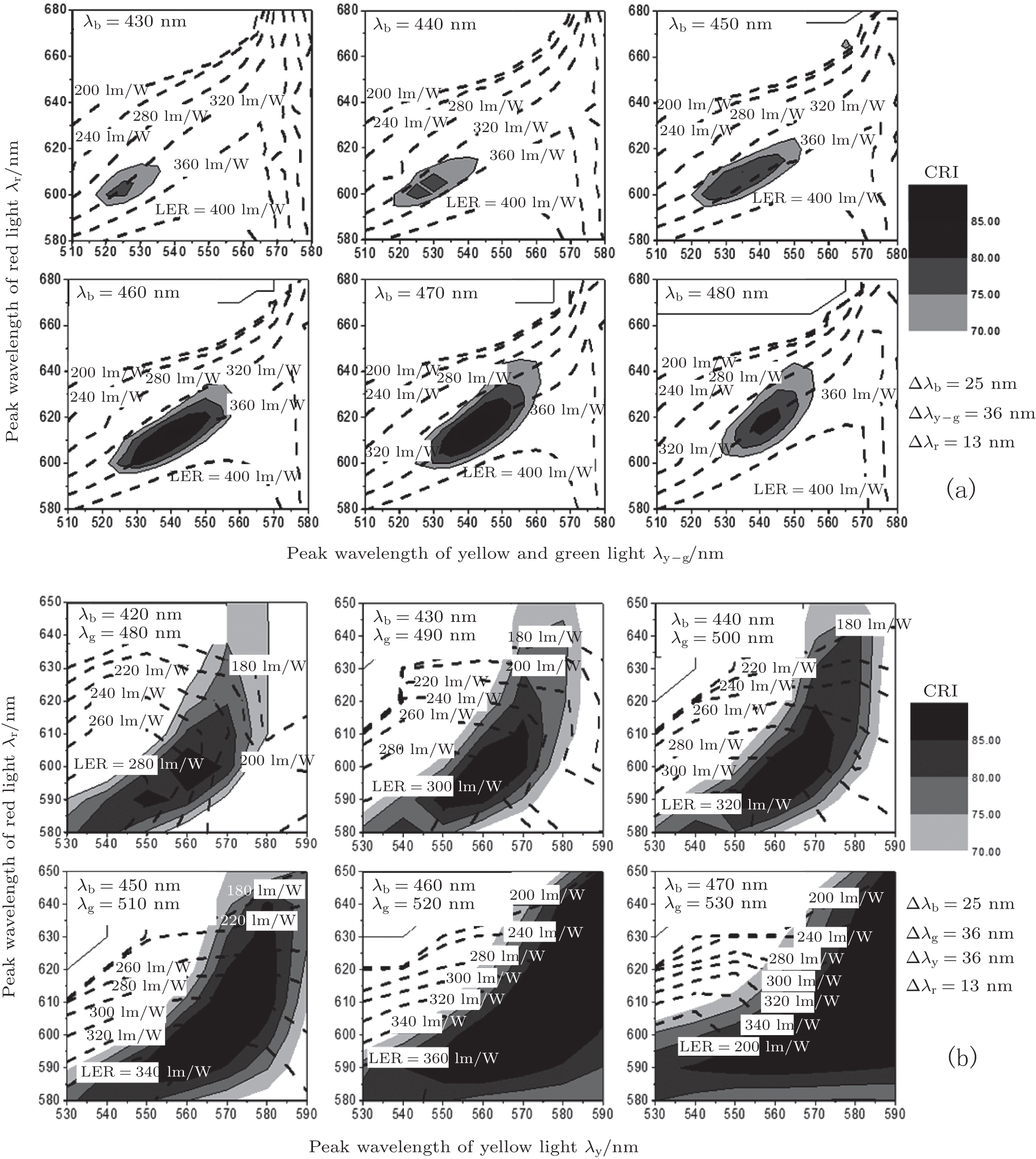 | Fig. 1. Dependence of LER and CRI of (a) tri-chromatic and (b) tetra-chromatic white LEDs on the different wavelength combinations of individual LEDs when the CCT is maintained at (5500± 20) K. |
Figure 1(b) shows the dependence of the calculated LER and CRI values of the tetra-chromatic white LEDs on the individual LEDs when the CCT is maintained at (5500± 20) K. The FWHM values are selected to be 25, 36, 36, and 13 nm. For the wavelength ranges from 450 nm to 470 nm, from 510 nm to 530 nm, from 560 nm to 590 nm, and from 590 nm to 620 nm, the CRI exceeds 80. When the wavelengths of the tetra-chromatic white LEDs are 460 nm, 520 nm, 570 nm, and 600 nm, the CRI reaches a maximum of 96.7 with an LER of 340 lm/W. When compared with the characteristics of the tri-chromatic white LEDs, the areas with CRI values of more than 80 for the tetra-chromatic white LEDs are much larger. In addition, when a redshift of the peak wavelength within 20 nm occurs because of Joule heating, the CRI can still remain above 80, which indicates that the CRI value for the tetra-chromatic scheme has better thermal stability.[35, 36] The narrow wavelength emission bands of these devices mean that the multiple color-matching scheme could improve the quality of the light source by increasing its spectral coverage.
The most direct way to create a monolithic phosphor-free white LED is based on the use of GaN. GaN-based white-light LEDs are particularly desirable because of their long lifetime, small size, and low consumption of energy, [25] because the band gap of InxGa1− xN ranges from approximately 3.5 eV to 0.64 eV at room temperature, with corresponding wavelengths ranging from the violet to infrared bands.[37] Theoretically, the entire visible wavelength band can be produced by a combination of InxGa1− xN/GaN MQWs with different indium contents and well widths, as shown in Fig. 2(a). However, because of the strong quantum confinement Stark effect and the solid phase immiscibility in the InxGa1− xN/GaN material system, which is a significant problem for typical InxGa1− xN epitaxial growth, the internal quantum efficiency of InxGa1− xN/GaN QWs is quite low for the green and red wavelengths.[38] In-phase separation and composition fluctuation were known to be related to the biaxial strain in InGaN layer grown on GaN and also to the miscibility gap between InN and GaN, which can shift notably into a higher In-content regime of the temperature-composition diagram.[39] Unintentional In-phase separations result in increased numbers of defects followed by dramatic degradation of the emission efficiency. In addition, the green and red wavelengths are close to the most sensitive regions of the human eyes, and affect the LER and CRI performances of LEDs considerably. According to the results of color-matching calculations, a mixture of blue and green light can generate a cool white light to the naked eye, which reduces the difficulty of growing InGaN with a high indium content. The conduction band diagram of blue and green MQWs is shown in Fig. 2(b). While In-phase separation was used further and was promoted by the composition pulling effect related to increments in the well thickness to produce green and amber emissions by In-phase separation in an InGaN single quantum well (SQW), [40] efficiency improvements for green emission from GaN-based LEDs have been widely investigated in recent years; particular focus has fallen on effective carrier injection against the carrier overflow mechanism, localized strain relaxation occurring through defects, and the dependence of the carrier recombination mechanisms on current injection.[41– 44]
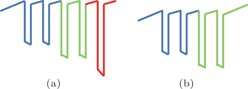 | Fig. 2. (a) Schematic conduction band diagram of RGB InGaN/GaN MQWs. (b) Schematic conduction band diagram of green and blue dual-wavelength InGaN/GaN MQWs. |
To improve the crystal quality of high-indium-content QWs and thus improve the quantum efficiency of the visible LED in the long wavelength range, a pre-strained InGaN layer with 7% In content was introduced underneath the subsequently deposited high-indium QWs, and led to LED output intensity enhancement of 56% for 120-mA current injection.[45] White light was obtained using blue and yellow light emissions with peak wavelengths of 465.7 nm and 549.1 nm from a monolithic LED.[46] However, the intensity of the green– yellow peak increased rapidly with increasing current injection from 10 mA to 60 mA, which resulted in a reduction in the CCT from 8037 K to 6062 K. The lower mobility of holes meant that the carrier filling level in each QW changed with increasing current injection, which resulted in the ratio of the peak intensities also changing with the current injection, especially when the number of QWs increased, as shown in Fig. 2(a). This phenomenon is known as the carrier transport effect, and it adversely affects the development of monolithic GaN-based LEDs, as does the difficulty of growing InGaN with high indium content.[47]
In addition to structures using InGaN/GaN MQWs, several other methods to produce white light based on monolithic GaN LEDs have been tried. InGaN/GaN MQWs that incorporated quantum dots capable of amber emission with two dominant emission peaks spanning from 1.7 eV to 2.2 eV were also unsuccessful attempts to circumvent the uniform carrier injection problem.[48] Laterally distributed blue and green InGaN/GaN MQWs that were grown by a selective area growth method were also proposed to overcome the problem of nonuniform carrier injection into the vertically stacked MQWs.[49] However, the required fabrication process is relatively complex.
The piezoelectric effect is important for AlGaInN materials because of the difference between the lattice constants of the InGaN active quantum wells (QWs) and the surrounding AlGaN layers.[50] A strong internal piezoelectric field induced by the quantum confined Stark effect separates the wave functions of the electrons and holes in quantum wells, which then reduces the radiation recombination probability of GaN LEDs on c-plane sapphire.[51, 52] Growth on r-plane 


The important technique of hybrid integration was successfully applied to hybrid lasers to provide optical signals for silicon photonic integrated circuits in the field of Si-based optical interconnections.[65, 66] Unlike RGB LEDs, for which color changes with viewing angle can be observed in a microscope because the light is emitted from three chips that are separated in space, vertically stacked RGB LEDs allow multiple colors to be mixed inside the chips and thus produce optimally mixed emission from the tops of the stacked LEDs.[67] In addition, quaternary AlGaInP alloys with their direct bandgap and lattice matching to GaAs are the most efficient light emitting materials produced in the 580 nm to 690 nm wavelength range to date.[68, 69] Because of the difficulty in producing green and amber emissions from InxGa1− xN/GaN MQWs, a series of hybrid integration methods using AlGaInP and InGaN MQWs have been proposed for high efficiency white light emission. For example, blue and green electrically-pumped InGaN LED chips coated with AlGaInP wavelength conversion layers generated white light with chromaticity coordinates of (0.338, 0.335) at 50 mA.[70] However, these devices were still subject to a wavelength conversion phenomenon that was similar to the Stokes shift effect in phosphor-based LEDs. The efficiency of the white light emission was also strongly dependent on the blue pumping wavelength, the absorption and the internal quantum efficiency of the light converter.[71]
Electrically-pumped devices are more convenient than optically-pumped devices. In addition to the electrically-pumped monolithic white LEDs that were reviewed in Section 3, the tunnel-regenerated multiple active region (TRMAR) structure can feasibly obtain multiple color emission by tuning of the indium content of each active region, which was initially proposed to obtain efficiencies higher than 1. A TRMAR AlGaInP LED was demonstrated in 2000 with double quantum efficiency for the LEDs with two active regions.[72, 73] The structure was then developed for organic LEDs and solar cells.[74, 75] Theoretically, the carrier injection level is the same in each active region, because of electron regeneration by the reverse-biased tunnel junctions. The combined electroluminescence (EL) spectrum from the multiple active regions does not change with current injection. Monolithic TRMAR dual-wavelength blue and green LEDs were first implemented in 2001, and emitted at 470 nm and 535 nm, respectively.[76] However, an efficient tunnel junction requires both a narrow energy band gap and a heavy doping density. The energy band gap of GaN is much larger than those of Si, Ge, and GaAs, which demonstrated efficient tunnel junctions, and it is also difficult to obtain highly doped p-type GaN. Therefore, the voltage drop across TRMAR GaN LEDs is relatively high, which in turn reduces the power efficiency of these devices.
To solve the difficulty of producing GaN tunnel junctions, and based on the TRMAR band structure, the hybrid integration of an InGaN MQW LED and an AlGaInP MQW LED was realized vertically using direct wafer bonding technology.[76] Under forward bias, spontaneous radiation recombination occurs in both InGaN MQWs and AlGaInP MQWs to generate white light with a specific power ratio. The carrier transport of the bonded p-GaAs/N-GaN heterojunction obeys the space-charge-limited conduction (SCLC) model, according to temperature-dependent current– voltage measurements which indicate that high density interface states exist at the bonding interface.[77] Figure 3(a) shows a schematic diagram of a hybrid integrated white LED structure. The tunnel junction was realized by the wafer bonding technique. Figure 3(b) shows the results of transmission electron microscopy (TEM) of the GaAs/GaN bonding interface. The top material is GaN and the lower material is GaAs with a 2-nm– 3-nm-thick bright layer sandwiched between these materials. The disordered lattice structure of this bright layer reveals an amorphous structure caused by the bonding process. After wafer bonding, the typical current– voltage curves of the hybrid integration-based white LED, the prebonded AlGaInP LED, and the InGaN LED are shown in Fig. 3(c). At 20 mA, the typical voltage drop of the white LED was approximately 10.6 V. The voltage drops of the prebonded AlGaInP LED and the InGaN LED at 20 mA were about 2.2 V and 4 V, respectively. The voltage drop across the bonding interface of the p-GaN/p-GaAs was as much as 3 V– 4 V, which is the main reason for the high voltage of the bonded LED. Figure 3(d) shows the EL spectrum of the hybrid integrated white LED at room temperature for currents ranging from 10 mA to 40 mA. At 20 mA, the peak wavelengths were located at 488 nm and 637 nm for the InGaN/GaN and AlGaInP MQW emissions, respectively. The redshifts of the cyan and red emissions were approximately 7 nm and 11 nm, respectively, and were caused by heating during device operation, caused by a much higher operating voltage. The optical power ratio between the blue and red portions of the emission was approximately 1.5, which was consistent with the results of dual color-matching calculations. However, because of the additional voltage, which reduced the power conversion efficiency, the chromatic stability also decreased with increasing current injection, as shown in Fig. 3(e).
 | Fig. 3. (a) Schematic diagram of the structure of the flip-chip hybrid integrated white LED, which was composed of InGaN/GaN and AlGaInP/GaAs MQWs. (b) TEM image of the GaN and GaAs bonding interface with a 2-nm– 3-nm-thick amorphous layer located between the two surfaces. (c) I– V curves of a hybrid integrated white LED and the individual LEDs before bonding. (d) EL spectra of the hybrid integrated white LED with current injection from 10 mA to 40 mA. (e) Chromatic coordinates of the hybrid integrated white LED under current injection in the range from 10 mA to 40 mA. |
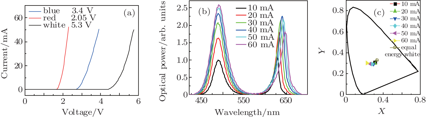 | Fig. 4. (a) I– V curves of hybrid integrated white LED and individual LEDs before bonding with a transparent conductive material. (b) EL spectra of the hybrid integrated white LED under current injection from 10 mA to 60 mA. (c) Chromatic coordinates of the hybrid integrated white LED under current injection ranging from 10 mA to 60 mA. |
To further reduce the bonding voltage and the thermal dissipation, a transparent conductive material is applied between the GaN LED and the flip-chip AlGaInP LED, creating a sandwiched device that has performance that is very sensitive to temperature. Figure 4(a) shows the I– V curves of the bonded white LED and the individual InGaN and AlGaInP LEDs. At 20 mA, the additional voltage caused by the bonding process is less than 0.5 V, which is considerably reduced. Then, the EL spectra of these white LEDs over the current range from 10 mA to 60 mA, which are shown in Fig. 4(b), change little with increasing current injection. The chromatic coordinates also change little with current, as shown in Fig. 4(c). Realization of a low-voltage hybrid integration-based white LED offers the possibility of commercially-produced phosphor-free white LEDs. However, many challenges have still to be investigated, including how to integrate three or more colors for high CRI values, and thermal management problems when vertically stacking three or more LED chips, which is especially important for high power LED chips.
In this review paper, we have discussed the interesting research in the field of phosphor-free white LEDs. Many interesting proof-of-concept phosphor-free white LEDs have been fabricated, and many new techniques have been developed for the realization of these devices. Theoretically, it is clear how the optical quality of white LEDs can be improved. However, to date, all proposals for phosphor-free white LEDs are still carried out under laboratory conditions and follow the dual-color scheme. It remains a considerable challenge to obtain commercial white LEDs with high efficiency without sacrificing CRI performance. Hybrid integration, which is now one of the most important methods in the field of Si photonics, could be one effective direction for the development of white LEDs, especially after the reduction of the additional bonding voltage. Such a structure is also suitable for vertical integration of multiple color LEDs to produce high CRI values by electrical pumping. We are confident that phosphor-free white LEDs will see exciting new developments and find practical applications over the next few years.
| 1 |
|
| 2 |
|
| 3 |
|
| 4 |
|
| 5 |
|
| 6 |
|
| 7 |
|
| 8 |
|
| 9 |
|
| 10 |
|
| 11 |
|
| 12 |
|
| 13 |
|
| 14 |
|
| 15 |
|
| 16 |
|
| 17 |
|
| 18 |
|
| 19 |
|
| 20 |
|
| 21 |
|
| 22 |
|
| 23 |
|
| 24 |
|
| 25 |
|
| 26 |
|
| 27 |
|
| 28 |
|
| 29 |
|
| 30 |
|
| 31 |
|
| 32 |
|
| 33 |
|
| 34 |
|
| 35 |
|
| 36 |
|
| 37 |
|
| 38 |
|
| 39 |
|
| 40 |
|
| 41 |
|
| 42 |
|
| 43 |
|
| 44 |
|
| 45 |
|
| 46 |
|
| 47 |
|
| 48 |
|
| 49 |
|
| 50 |
|
| 51 |
|
| 52 |
|
| 53 |
|
| 54 |
|
| 55 |
|
| 56 |
|
| 57 |
|
| 58 |
|
| 59 |
|
| 60 |
|
| 61 |
|
| 62 |
|
| 63 |
|
| 64 |
|
| 65 |
|
| 66 |
|
| 67 |
|
| 68 |
|
| 69 |
|
| 70 |
|
| 71 |
|
| 72 |
|
| 73 |
|
| 74 |
|
| 75 |
|
| 76 |
|
| 77 |
|