
Gate dependent photoresponse in self-assembled graphene p–n junctions*
[Yin Wei-Hong, Yu-Bing Wang, Han Qin† , Yang Xiao-Hong]
, Yang Xiao-Hong]
|
|


†Corresponding author. E-mail: hanqin@semi.ac.cn
*Project supported by the High Technology Research and Development Program of China (Grant No. 2013AA031401), the National Natural Science Foundation of China (Grant Nos. 61176053, 61274069, and 61435002), and the National Basic Research Program, China (Grant No. 2012CB933503).
The intrinsic photocurrent generation mechanism of a self-assembled graphene p–n junction operating at 1.55 μm is investigated experimentally. It is concluded that both a photovoltage effect and a photothermoelectric effect contribute to the final photocurrent. The photocurrent signal at the p–n junction was found to be dominated by photothermoelectric current, arising from different self-assembled doping levels.
Graphene, a single layer of carbon atoms arranged in a hexagonal honeycomb lattice, has a linear energy dispersion relation, resulting in a vanishing effective mass and a high Fermi velocity (about 1/300 of the speed of light). It has ultrahigh electrical mobility which can approach 2× 105 cm2· V− 1· s− 1 for both electrons and holes.[1] Moreover, graphene has equally remarkable optoelectronic properties. Graphene can uniformly absorb 0.23% of incident light over a wide range, from visible to infrared. Considering the single-layer nature of graphene, the absorption efficiency is very high when compared to bulk material with an equivalent thickness.[2] Benefiting from its superior electronic and photonic properties, graphene has extensive applications in optoelectronic devices, [3] such as solar cells, [4] light-emitting devices, [5] touch screens, [6] terahertz, [7, 8] plasmonic devices, [9, 10] photodetectors, [11, 12] modulators, [13] and ultrafast lasers.[14]
Photodetectors are key components for communication systems. Graphene integrated photodetectors can potentially operate at speeds over 500 GHz, [11] which also have small footprints and are compatible with complementary metal– oxide semiconductor (CMOS) processing.[15] In the previously reported graphene photodetectors (G-PDs), the photocurrent response regimes are attributed to the conventional photovoltaic (PV) effect[16] in graphene– metal contacts or p– n junctions.[17] Photothermoelectric (PTE) effect[18] induced photocurrent was also identified at a graphene interface junction.[19] Graphene photodetectors based on bolometric effects have also been demonstrated.[20] Recently, graphene p– n junctions have attracted strong interest, owing to the possibility to validate the intrinsic photoresponse regimes in graphene. The preparation of graphene p– n junction is usually complex chemical doping[21] or dual gated.[22] Here, we demonstrate a self-assembled graphene p– n junction and investigate its intrinsic optoelectronic responses.
Graphene devices consisting of single layer graphene were fabricated by mechanical exfoliation of graphite sheets onto an SiO2/Si wafer. First, a silicon substrate (0.1 Ω · cm) covered with a 300-nm thermal oxidation silica layer was cleaned in H2SO4+ H2O2 solution, changing the silicon oxide from hydrophobic to hydrophilic, which can improve the stability of graphene on the substrate. The doped silicon substrate acted as a back gate. Then, single layer graphene flakes, which were prepared by mechanical exfoliation of graphite crystal, were transferred onto the SiO2/Si substrate. After the material was identified and confirmed by microscope and Raman spectroscope (λ exc= 488 nm), [23] we performed electron beam lithography to pattern the source and drain contact electrodes. Finally, metal films of Ti/Au (20 nm/70 nm) were deposited and lifted off in acetone.
Photocurrent measurements were carried out under ambient condition using a semiconductor parameter analyzer at zero source drain bias. We used a tapered cylindrical optical fiber to focus the laser source. The light source is a DFB laser operating at a wavelength of 1550 nm, amplified by an erbium-doped fiber amplifier (EDFA) and calibrated by an optical power meter. We defined a positive current flowing from the source to the drain. Sweeping the gate voltage, we got photocurrent (PC) curves similar to those reported before[12] when the light was focused near the metal contact. Here, we paid more attention to whether there was a photocurrent when the light was focused on the graphene channel away from the metal contact. In most of the devices there was no photocurrent in the channel. In a few devices, we got a novel photoresponse when the light was focused on two specific positions of the graphene channel and merely an almost non-existent photocurrent on the other area away from the two specific regions. The novel result is shown in Fig. 1 (we designated the device “ Die 1; ” it has a 13-μ m long graphene channel), the two PCs generated in positon 1 and position 2 were noted as PC-L and PC-R (the two PC generation regions are pointed out in the inset schematics). Figure 1 shows that the two phototcurrent curves are symmetrical in morphology and that the sign reverses twice while sweeping the gate voltage. They show a peak value at a gate voltage of 9 V.
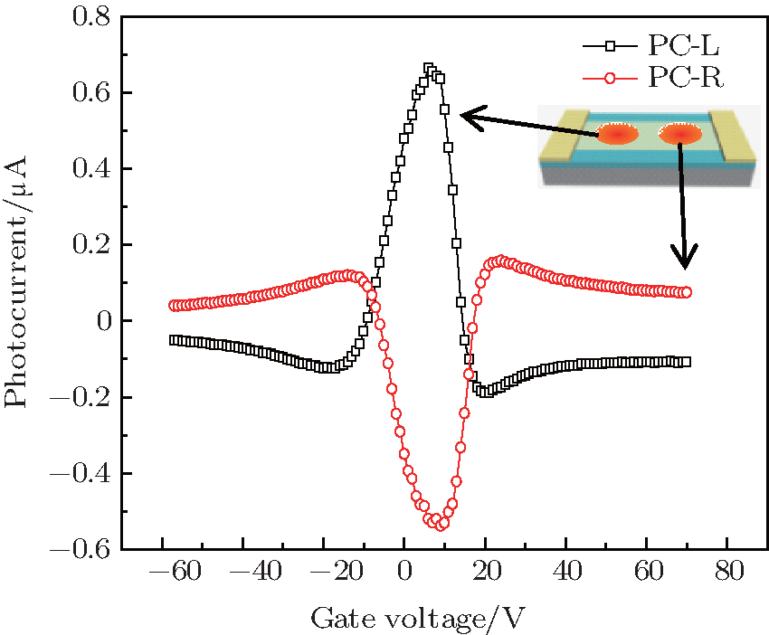 | Fig. 1. Gate-dependent photoresponse of Die 1; inset: the photocurrent generation position. |
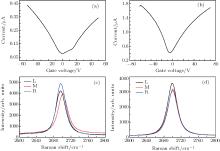
To investigate the intrinsic optoelectronic response of this novel phenomenon, we need to confirm the intrinsic properties of the devices. We employed a conventional device which had no photocurrent when the light focused on the graphene channel as a contrast (noted as Die 2 which has a 15-μ m long channel length). First, fundamental transfer characteristics measurements were performed to evaluate the electronic properties of our devices. Die 2, as reported previously, [24] has one minimum point of source drain current at the gate voltage of − 5 V in its transport curve, as shown in Fig. 2(b). In the transport curve of Die 1, as exemplified by Fig. 2(a), the charge-neutralized point (CNP) of graphene is at Vg = − 1 V, indicating the n-doping of graphene. Moreover, an additional dip appears at Vg = 17 V indicating the graphene is partially p-doped. Thus a p– n junction is formed in the middle of the graphene channel.[25] Graphene is very sensitive to circumstances. Going through the same fabrication process, it may display different doping levels, sometimes in one specific flake. To further corroborate them, we used a Raman microscopy (λ exc= 488 nm) method to detect the shift of two-dimensional (2D) peaks in different areas of the graphene channel in each device, which can imply varying doping levels of the graphene channel. The G peak stiffens and sharpens for both electrons and holes doping, however the 2D peak shows a different response to holes and electrons, making it a sensitive parameter to monitor the doping.[26] The results are shown in Fig. 2(c) (Die 1) and Fig. 2(d) (Die 2). The letters L, M, and R represent the left, middle, and right sections of the graphene channel, respectively. For Die 2, the positions of the 2D peak for different parts of the graphene channel are nearly the same. One can find there are slight changes in positions of the 2D peak. This is due to electron– hole puddles and unintentional doping. However, for Die 1, the position of the 2D peak shifts somewhat from 2694 cm− 1 for both L and R to 2701 cm− 1 for M, indicating varied doping levels for L, R, and M. Seven-wave numbers red shifting means an obvious doping level change. The higher value of the 2D peak wave number corresponds to a lower Fermi energy.[26] Combining with Fig. 1, this seven-numbers red shift indicates a p doping of the middle position of Die 1, thus creating two back-to-back pn− junctions in the graphene channel.
After getting the intrinsic doping type of the devices, we find that the novel PC mainly results from the self-assembled p– n junction. As the devices were tested under zero source drain bias, the photocurrent generation mechanism is possibly PV effect or PTE effect, [20] where both of them may contribute to the final photocurrent. Obviously, in Fig. 1, the photocurrent presents multiple photocurrent sign changes as a function of gate voltage at zero source drain bias. This is a clear indication of photocurrent generation from the thermoelectric effect.[18]
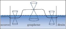
Figure 3 is a schematic plot of the back-to-back junctions at zero gate voltage. The two junctions have the same properties and represent symmetric photocurrent versus gate voltage curves. We focused at one junction to show its PC generation mechanism. As for the different doping levels, there are potential steps in p– n junctions. When the light focuses on the junction, it generates photo-induced carriers which separate by the built-in field, and the PV effect induces photocurrents. The Seebeck parameter of the p and n areas in the junction are different. PET-induced photocurrent also exists. The detected current is the combination of the two PCs. When changing the gate voltage, the junctions present p– p+ , p– n, n– n+ doping types. The doping level of the total graphene channel changes when serving a back gate voltage; the potential steps will not change direction in this three-doping type, because of which the PV effect current presents one polarity under faculative gate voltage. PTE effect current is sensitive to the temperature gradient of the two regions and also to the Seebeck parameter difference of the corresponding areas. It can be given by the following formula:

S is the Seebeck coefficient and is given as follows:

where G is conductance and kB is the Boltzmann constant. In the p– n junction, the PTE effect current and the PV effect current show the same polarity and in the unipolar junction regimes p– p+ , n– n+ , the two effects show opposite polarity, so the photocurrent switches sign twice with gate voltage sweeping.[22] This mechanism leads to a PTE-dominated photocurrent in Die 1 (Fig. 1(b)).
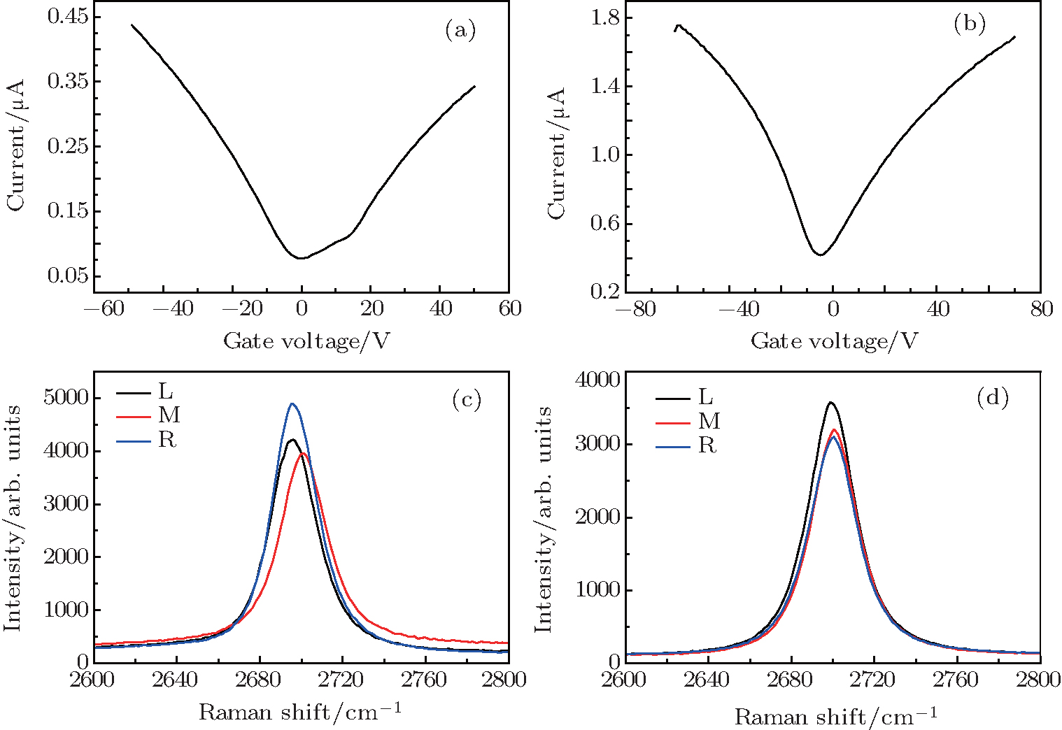 | Fig. 2. Transfer characteristics of Die 1 (a) and Die 2 (b); the Raman shift of Die 1 (c) and Die 2 (d). |
 | Fig. 3. Potential profile in self-assembled p– n junctions at zero gate voltage, the dotted line represents the Femi level. |
In summary, we experimentally demonstrated a novel self-assembled graphene p– n junction photodetector using single layer graphene. It is found that both the photovoltage-effect-induced photocurrent and photothermoelectric current contribute to the total photoresponse of graphene PDs. The gate-dependent photocurrents of self-assembled p– n junctions are dominated by the photothermoelectric effect.
| 1 |
|
| 2 |
|
| 3 |
|
| 4 |
|
| 5 |
|
| 6 |
|
| 7 |
|
| 8 |
|
| 9 |
|
| 10 |
|
| 11 |
|
| 12 |
|
| 13 |
|
| 14 |
|
| 15 |
|
| 16 |
|
| 17 |
|
| 18 |
|
| 19 |
|
| 20 |
|
| 21 |
|
| 22 |
|
| 23 |
|
| 24 |
|
| 25 |
|
| 26 |
|