

Influence factors and mechanism of emission of ZnS:Cu nanocrystals*
[Chu Xue-Yinga) , Wang Xin-Nonga) , Li Jin-Hua†a)  , Yao Dan
a) , Fang Xuana), b) , Fang Fanga), c) , Wei Zhi-Pengb) , Wang Xiao-Huab) ]
, Yao Dan|
|

 , Yao Dan
†Corresponding author. E-mail: jhli cust@163.com
*Project supported by the National Natural Science Foundation of China (Grant Nos. 61205193, 61204065, and 61307045), the Specialized Research Fund for the Doctoral Program of Higher Education of China (Grant No. 20112216120005), and the Developing Project of Science and Technology of Jilin Province, China (Grant Nos. 201201116, 20140520107JH, and 20140204025GX).
Copper-doped ZnS (ZnS:Cu) nanocrystals are synthesized by the sol–gel method. The average size of the ZnS:Cu nanocrystals is 3.1 nm. The x-ray diffraction indicates that increasing the Cu-dopant concentration results in a large shift in the diffraction angle. The effects of the dopant concentration, the reactant ratio, and aging temperature on the optical properties of the ZnS:Cu nanocrystals are also investigated. The fluorescence emission mechanism is analyzed by peak deconvolution using Gaussian functions. We find that the emission of the ZnS:Cu nanocrystal is composed of different luminescence centers at 430, 470, 490, 526, and 560 nm. The origins of these emissions are discussed and demonstrated by controlled experiments.
ZnS is a typical luminescent II– VI semiconductor, with a direct band gap of 3.5 eV– 3.8 eV.[1] It has been used in light emitting diodes, [2, 3] photovoltaic devices, [4] and biological markers.[5] Rare earth or transition metal ions (e.g., Mn, [6] Cu, [7] and La[8]) can be used as activators, to change the internal energy structure of the ZnS matrix. Different luminescence levels can therefore be introduced, and the optical properties can be modified accordingly. Doping ZnS nanocrystals with Mn2+ yields orange (∼ 590 nm) emission, [9] the origin of which has been well studied. Compared with ZnS:Mn, ZnS:Cu nanocrystals can provide multi-color emission in the visible region (from blue to green), [10] and have aroused much interest in biological fields.[11]
ZnS:Cu nanocrystals can be prepared by different methods, and much effort has focused on characterizing their optical properties. However, the origin and mechanism of their emission remain unclear. For example, Sambasivam et al. obtained ZnS:Cu nanopowder with an average particle size of 8.5 nm, by colloidal chemistry coprecipitation method. They found that the emission peak wavelength decreased with increasing the Cu-dopant concentration.[12] Whereas, the emission of ZnS:Cu nanocrystal (∼ 3 nm) synthesized by Corrado et al. did not vary with dopant concentration.[13] One possible reason of the divarication might be imputed to the different preparation procedures used. Nanomaterial synthesis conditions can significantly influence their structures, sizes, and optical properties. Investigating the influence of such factors under controlled experimental conditions is conducible to our understanding of their emission mechanism.
In the present study, Gaussian fitting is used to infer the emission mechanism of ZnS:Cu nanocrystals which are prepared by the sol– gel method. The experimental conditions are altered in a controlled manner. The hypothesis of the mechanism is confirmed by the influence of specific conditions on the optical properties.
The 0.174-mL 3-mercaptopropionic acid (MPA) was added to 5-mL of aqueous 0.1-M Zn(CH3COO)2· 2H2O. This solution was diluted to 44 mL with water. 0.1 mL of 0.1-M Cu(CH3COO)2· H2O was added, to achieve a dopant concentration of 2%. The pH was adjusted to ∼ 10, by the dropwise addition of NaOH. Five milliliters of aqueous 0.1-M Na2S· 9H2O was quickly injected under vigorous stirring. The reaction mixture was mechanically agitated for 15 min with a rotational speed 125 r/min, and then further shaken for 2 h at 45 ° C to age the sample. A transparent solution containing ZnS:Cu nanocrystals was obtained. ZnS nanocrystals were also prepared similarly for comparison.
Various experimental conditions were changed to investigate their influence on the optical properties of the product. The volume of the Cu(CH3COO)2· H2O solution was increased to 0.2 mL and 0.4 mL, yielding ZnS:Cu nanocrystals with 4% and 6% dopant concentrations, respectively. The volume of the Na2S· 9H2O solution in the above synthetic process was 5 mL, giving a Zn2+ /S2− ratio of 1:1. This volume was varied at 2 mL or 8 mL, to give a Zn2+ /S2− ratio of 5:2 or 5:8. The aging temperature was also changed from room temperature (RT) to boiling temperature (BT).
Crystal structures were investigated from x-ray diffraction (XRD) patterns recorded with a Rigaku D/MAX2500 diffractometer, using the 0.1541-nm Cu Kα line. The morphology and size of the particles were observed by transmission electron microscopy (TEM) using a JEM-2100 microscope. Optical properties were investigated from ultraviolet-visible (UV-Vis) absorption spectra recorded on a UV-2450PC Shimadzu spectrophotometer. Fluorescence spectra of the ZnS:Cu samples were collected using an RF-5301PC spectrophotometer. The wavelength of the excitated light is 310 nm for all emission spectrum collection.
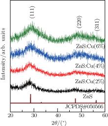
XRD patterns of the ZnS and ZnS:Cu nanocrystals are shown in Fig. 1. Three diffraction peaks are observed, corresponding to the (111), (220), and (311) lattice planes of a cubic zinc blended structure. This result correlates well with Joint Committee on Powder Diffraction Standards (JCPDS) card no. 05-0566. No other diffraction peaks are observed in the patterns of all samples, indicating no obvious impurities. Increasing the Cu-dopant concentration results in large shifts in a diffraction angle. The positions of the (111) peaks of undoped ZnS, ZnS:Cu (2%), ZnS:Cu (4%), and ZnS:Cu (6%) nanocrystals are located at 27.9° , 28.2° , 28.8° , and 29.3° , respectively. The Cu2+ radius (0.72 Å ) is smaller than that of Zn2+ (0.74 Å ). If the introduced Cu2+ ions are substituted for the Zn2+ , the interplanar distance will be reduced. Thus, the increasing of 2θ angle reflects the decreasing of interplanar distance.
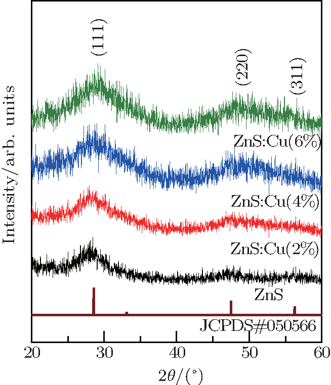 | Fig. 1. XRD patterns of ZnS and ZnS:Cu nanocrystals, and standard JCPDS no. 050566 data. |
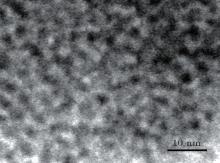
To study the morphology and the size, a TEM image of the 2% Cu-doped ZnS nanocrystals is shown in Fig. 2. The particle size distribution of the ZnS:Cu nanocrystals is narrow and the average size is 3.1 ± 0.1 nm.
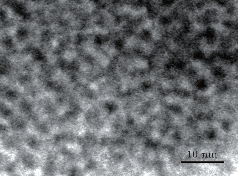 | Fig. 2. TEM image of the 2% doped ZnS:Cu nanocrystals. |
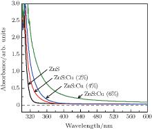
The UV-Vis absorption and fluorescence spectra of the ZnS:Cu nanocrystals are shown in Figs. 3 and 4. The data of the undoped ZnS nanocrystals are also displayed for comparison. As shown in Fig. 3, the absorption edge of the ZnS nanocrystals occurs at 315 nm. Introducing 2%, 4%, and 6% Cu2+ cause the absorption edge to red-shift to ∼ 328, 335, and 355 nm, respectively. Doping with Cu2+ may result in lattice distortion or other defects, yielding the shifts of absorption spectra. This hypothesis is supported by the more pronounced red-shift at the absorption edge with increasing the Cu2+ concentration.
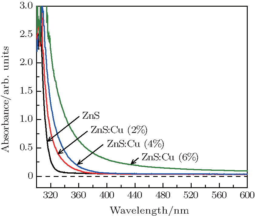 | Fig. 3. UV-Vis absorption spectra of ZnS and ZnS:Cu nanocrystals. |
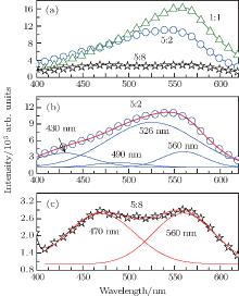
Various experimental parameters are then changed to investigate their influences on the fluorescence emission spectrum. The influence of dopant concentration is first discussed. The emission spectra of ZnS:Cu nanocrystals with different dopant concentrations are shown in Fig. 4. Samples are directly added to the cuvettes without being diluted in the measurement, to allow their intensities to be directly compared. Figure 4(a) shows that the ZnS:Cu (2%) nanocrystals exhibit the highest emission intensities. The increasing of the dopant concentration reduces the emission intensity. ZnS:Cu nanocrystals with a dopant concentration of 1% are also prepared to confirm that 2% is an optimal concentration. This decline can be explained by “ concentration quenching” , which is common in fluorescent materials.[14]
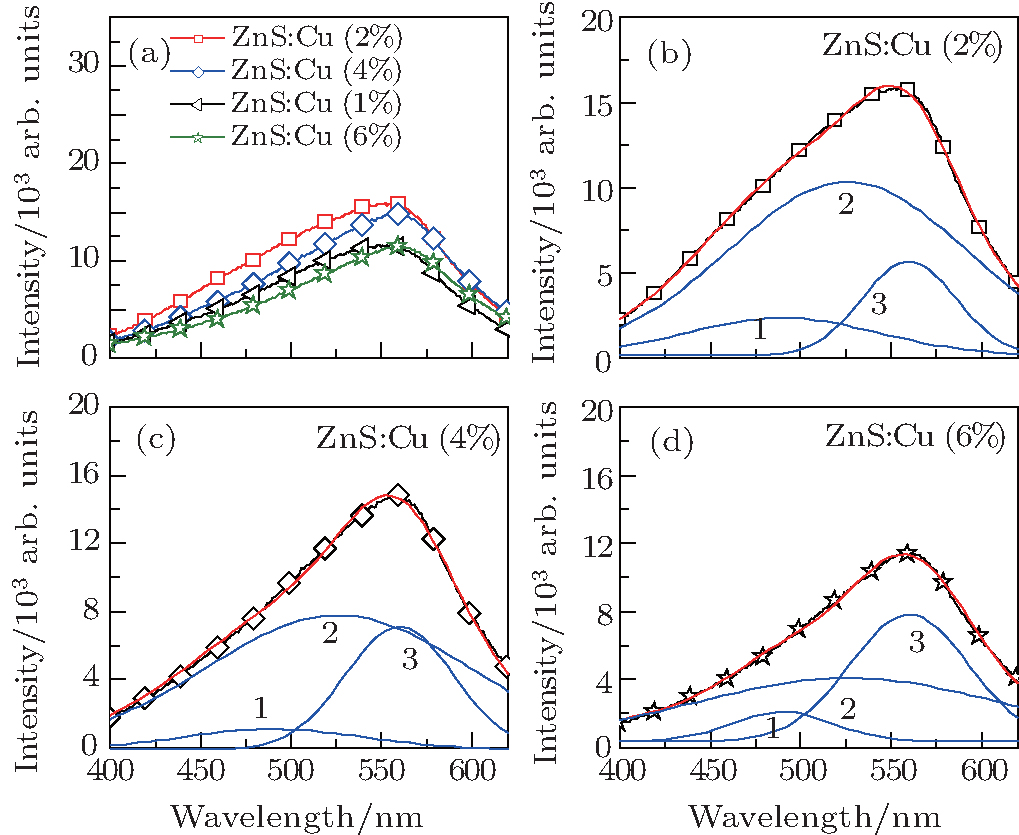 | Fig. 4. (a) Emission spectra of ZnS:Cu nanocrystals with different dopant concentrations. Gaussian fitting of emission spectra of ZnS:Cu nanocrystals with the dopant concentrations of (b) 2%, (c) 4%, and (d) 6%. |
The emission peaks of the ZnS:Cu nanocrystals with different dopant concentrations are all centered around 550 nm, and are all asymmetric. Peak deconvolution by using Gaussian functions is useful for understanding the origin of such asymmetric emission.[15– 17] All emission peaks are well fitted by three Gaussian peaks at 490, 526, and 560 nm as shown in Figs. 4(b)– 4(d). Defects play an important role in the luminescence of ZnS nanocrystals. Sulfur vacancies and interstitial zinc atoms are reported to be in donor states, whereas zinc vacancies and interstitial sulfur atoms lead to acceptor states.[18] Because of the different binding energies, interstitial sulfur states are usually located closer to the valence band than interstitial zinc states approach to the conduction band.[19] The distance between sulfur vacancies and the conduction band edge is also smaller than that between zinc vacancies and the valence band edge.[20] The luminescence at 490 nm is attributed to the recombination of the energy level of sulfur vacancies with interstitial sulfur states, [20] so is unrelated to Cu doping. This conclusion is supported by the emission intensity at 490 nm, which is less than those at 526 nm and 560 nm. The emission intensity at 526 nm is likely to result from the radiative transition between the conduction band and the t2 level of Cu2+ , [21] and that at 560 nm is associated with the recombination between the deep donor level and the t2 level of Cu2+ .[22] The emission intensities at 526 nm and 560 nm exhibit opposing trends to the dopant concentration. Increasing Cu2+ concentration gradually induces the emission to decrease at 526 nm, but increase at 560 nm. As mentioned above, the overall emission intensity decreases with increasing the Cu2+ concentration. Thus, the emission at 526 nm is dominant in the present ZnS:Cu system. The slight enhancement in emission at 560 nm indicates that the deep donor level in ZnS:Cu is related to the Cu2+ doping.
 | Fig. 5. (a) Emission spectra of ZnS:Cu nanocrystals prepared under Zn2+ :S2 ratios of 5:2, 1:1, and 5:8. Gaussian fitting results of the emission spectrum marked by (b) 5:2 and (c) 5:8. |
The influence of the Zn2+ :S2 ratio on emission is also analyzed to further elucidate the emission mechanism. Figure 5(a) shows the fluorescence spectra of ZnS:Cu nanocrystals prepared from Zn2+ :S2 ratios of 5:2, 1:1, and 5:8. The maximum emission intensity is exhibited by the 1:1 sample, probably because more non-radiative centers form when the Zn2+ :S2 deviates from 1:1. The products containing excess Zn2+ ions (i.e., Zn2+ :S2 of 5:2) require an extra emission peak at 430 nm for satisfactory Gaussian fitting as shown in Fig. 5(b). This result and the analysis reported in the literature suggest that the emission at 430 nm is related to sulfur vacancies.[23] When S2− is excess (i.e., Zn2+ :S2 of 5:8), the most possible defects may be in the form of zinc vacancies. The Gaussian fitting result indicates that it can be well fitted by two emission peaks at 470 nm and 560 nm as shown in Fig. 5(c). The reported data support the emission peak at 470 nm, which is related to zinc vacancies.[24]
Based on the above analysis, a possible emission mechanism of the ZnS:Cu nanocrystals is depicted in Fig. 6.
 | Fig. 6. Energy level diagram of ZnS:Cu nanocrystals. |
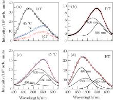
To confirm the emission mechanism, the influence of aging temperature on emission is also investigated. Figure 7(a) shows the emission spectra of ZnS:Cu nanocrystals aged at RT, 45 ° C, and BT. The emission spectra are asymmetric, and Gaussian fitting results are shown in Fig. 7(b)– 7(d). The sample aged at RT is fitted by two Gaussian peaks at 526 nm and 560 nm as shown in Fig. 7(b). The ZnS:Cu nanocrystal aged at 45 ° C requires an extra emission component at 490 nm for satisfactory fitting as shown in Fig. 7(c). According to the above hypothesis of the mechanism, the emission at 490 nm is associated with sulfur vacancies. Oxidation of surface S2− is probable, so it is logical that more sulfur vacancies form at higher temperature. Further increasing the aging temperature would lead to more vacancy defects, including zinc vacancies and sulfur vacancies. Figure 7(d) shows that the emissions at 470 nm and 490 nm significantly increase when the sample is aged at BT. As shown in Fig. 6, the wavelengths of the zinc vacancies and sulfur vacancies defect-related emissions are just at 470 nm and 490 nm. This supports the current assignment of emission centers.
 | Fig. 7. (a) Emission spectra of the ZnS:Cu nanocrystals aged at RT, 45 ° C, and BT. Gaussian fitting results of the emission spectrum marked by (b) RT, (c) 45 ° C, and (d) BT shown in panel (a). |
ZnS:Cu nanocrystals are prepared by the sol– gel method. The influences of dopant concentration, reactant ratio, and aging temperature on the optical properties of the ZnS:Cu nanocrystals are studied. Gaussian fitting is used to deconvolute the emission spectra of the ZnS:Cu nanocrystals into components at 430, 470, 490, 526, and 560 nm. An integrated comparison indicates that the present ZnS:Cu nanocrystal exhibits a strongest Cu2+ -related emission when the dopant concentration is 2%, Zn2+ :S2 is 1:1, and aging temperature is 45 ° C.
| 1 |
|
| 2 |
|
| 3 |
|
| 4 |
|
| 5 |
|
| 6 |
|
| 7 |
|
| 8 |
|
| 9 |
|
| 10 |
|
| 11 |
|
| 12 |
|
| 13 |
|
| 14 |
|
| 15 |
|
| 16 |
|
| 17 |
|
| 18 |
|
| 19 |
|
| 20 |
|
| 21 |
|
| 22 |
|
| 23 |
|
| 24 |
|