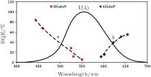
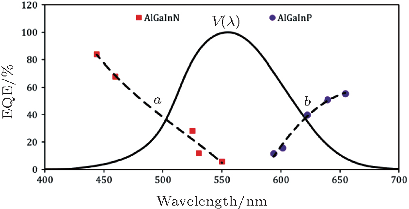
1. IntroductionWith the fast development of light-emitting diodes (LEDs) in recent years, as solid state lighting greatly influences people’ s lives, the LEDs have been widely used in general lighting, large scale displays, indicator lights, electronic devices’ backlights, etc. The prosperity of LEDs can be attributed to the success of GaN-based blue LEDs, which was first realized in the 1990s.[1] Since then, GaN-based LEDs have become more and more efficient, and have finally been adopted in white lighting. The current LED lighting is based on phosphor conversion of blue LEDs, which has limited efficiency, high cost, and insufficient illumination quality. By mixing highly efficient LEDs of different colors to form white light, there will be huge potential on efficiency improvement with much better illumination quality. The key to successful color mixing for white light is to enhance the efficiency of LEDs in the long wavelength range, specifically the green LEDs. Theoretically, the emission spectra of the AlGaInN system cover the entire range of visible light. The AlGaInN system has shown its strength in blue light — the highest external quantum efficiency (EQE) goes beyond 80% for GaN-based blue LEDs.[2] They also have advantages in the green light range: 30% EQE is much higher than that of the conventional AlGaInP green LEDs. However, it still has great potential compared with blue LEDs. As shown in Fig. 1, the efficiencies of AlGaInN-based LEDs drop fast as wavelength increases from 450 nm to 550 nm, and the efficiencies of AlGaInP-based LEDs drop even faster as wavelength decreases from 650 nm to 600 nm. The efficiencies of LEDs are relatively low within the range from 500 nm to 600 nm, which is known as the “ green gap.” The peak of the CIE eye sensitivity function curve lies just in the center of the gap, implying low efficiencies for the sensitive colors. The purpose of developing GaN-based green LEDs is not only to increase the luminous efficiency of LEDs, but also to fill a blank emission region of visible light for solid state lighting.
Due to a transition of bandgap from direct to indirect as the aluminum content is increased in order to get shorter wavelengths, the efficiency of AlGaInP LEDs inherently decreases with decreasing wavelength; thus AlGaInP systems are not expected to fill the green gap. For AlGaInN green LEDs, the high indium content in InGaN quantum wells (QW) brings many unfavorable effects for LED efficiency. High indium content requires low growth temperature, which is unfavorable for the quality of the QW. Also, the QW becomes inhomogeneous due to limited intersolubility of InN and GaN, which causes potential fluctuation and even indium segregation. Furthermore, the piezoelectric field caused by lattice mismatch between the InGaN QW and GaN barrier becomes higher, which negatively impacts the efficiency of green LEDs.
In this paper, we will discuss the status of recent research into green LEDs and focus on the technologies of developing GaN-based green LED on Si substrate.
2. Status of the high efficiency GaN-based green LEDThe earliest green LEDs, which appeared in the 1970s, were based on nitrogen-doped GaP[4] with very low efficiency. Later, the AlGaInP system with better performance in the yellow– green to red spectral region was adopted, [5] but it cannot be used in the shorter wavelength range of green light. After the remarkable breakthroughs of GaN-based blue LEDs in the 1990s, [6– 9] the green LEDs progressed to a new stage. The early GaN-based green LEDs had simple active-layer structures[10– 12] and were little changed compared with blue LEDs, only increasing the indium content in the QW; the efficiency of those LEDs was relatively low. In 1995, Nakamura reported GaN-based blue, green, and yellow LEDs; [12] the EQEs were 7.3%, 2.1%, and 1.2%, respectively. After twenty years, the efficiency of blue LEDs raised quickly beyond 80%, and green LEDs’ efficiency also improved, with typical efficiency around 30%, but not as efficient as blue LEDs. Hence there is still great potential for GaN-based green LEDs. To improve the efficiency of green LEDs, it should be understood what affects the efficiency of LEDs. Despite leakage carrier, the IQE of an LED can be expressed simply as[13]

where A, B, C, and N are defect-related non-radiative recombination coefficient, radiative recombination coefficient, auger recombination coefficient, and carrier concentration in the active region, respectively. The total carrier consumption rate can be written in the form of current density

where J, q, and d are current density, elementary charge, and thickness of active region, respectively. The peak IQE (η max) and the corresponding current density (Jmax) can be deduced from the above equations:[14]


Assume the radiative recombination coefficient (B) and auger recombination coefficient (C) do not change at a constant temperature, better QW quality which means smaller non-radiative recombination coefficient (A) will lead to a higher peak IQE, and it also can be concluded that the corresponding current density is proportional to the thickness of the QW.
Figure 2 plots the typical curves of internal quantum efficiency (IQE) versus current density for both a blue LED and a green LED at room temperature (300 K). The biggest difference between the two curves is the blue LED has a higher peak IQE, which reaches as high as 92.9% at 7.5 A/cm2, while the green LED’ s peak IQE is 62.1% at 2 A/cm2.
Referring to the above discussion, the lower peak IQE implies a poorer QW quality for the green LED, which can be attributed to the high indium content and low growth temperature of green QW. That the current density of the green LED at its peak IQE is also lower than that of the blue LED implies a smaller effective active volume for the green LED.
Another important phenomenon is the decay of efficiency with injected current density, which is also known as efficiency droop, is different between green and blue LEDs. At working current density, mostly 35 A/cm2, the green LED suffers 30% decay from peak IQE, while the value for the blue LED is only 10%. The efficiency droop can be attributed to carrier leakage and/or auger recombination. Lattice mismatch between InGaN QW and GaN barrier leads to compression stress in QW and results in a polarization effect. A build in piezoelectric field can cause band bending and carrier delocalization, which increases the carrier leakage probability and lowers the radiative recombination efficiency. More indium content in the green LED means a higher piezoelectric field and higher carrier leakage probability. Therefore, it is reasonable to observe a more severe droop in the green LED.
In short, the key to improving green LEDs’ efficiency can be simplified into two points: improve the QW quality and reduce the piezoelectric field. Many studies that were carried out to improve green LEDs’ efficiency focus on these two points.[14– 18] Some are selectively introduced below.
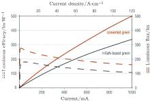
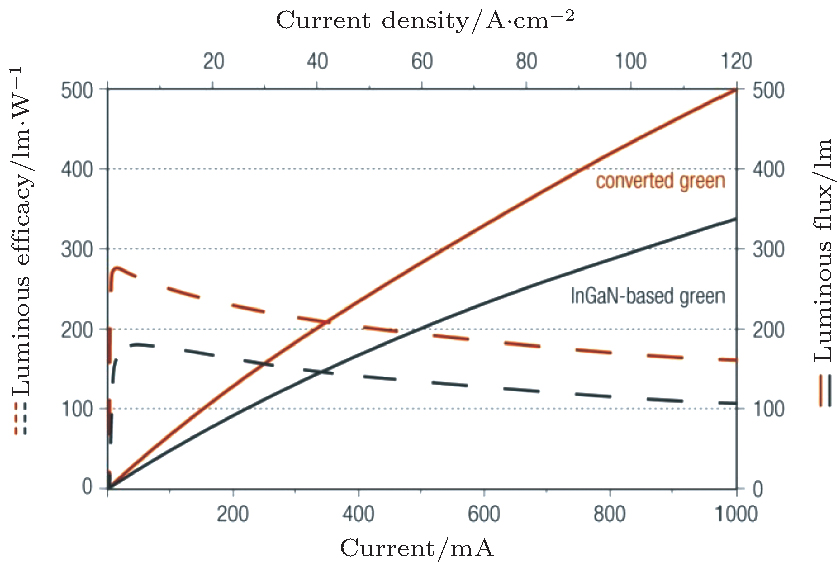
2.1. Phosphor-converted green LEDSince blue LEDs are very highly efficient, a common method of obtaining green LEDs is to convert blue LEDs to green using phosphor. Definitely, there will be energy lost as high energy blue light is converted to lower energy green light. Even if the phosphor-converting efficiency is 100%, there will be at least 10% energy lost. However, as the efficiency of current green LEDs is too low, converting blue LEDs to green LEDs is still a practical way to obtain highly efficient green LEDs. For example, Osram released its results of green LEDs recently, [19] as shown in Fig. 3. At 42 A/cm2, a direct GaN-based green LED achieves an efficiency of 147 lm/W, which is a remarkable result, but the converted green LED has an even higher efficiency of 209 lm/W. Therefore, the phosphor-converted green LEDs are more efficient than direct GaN-based green LEDs so far.
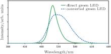
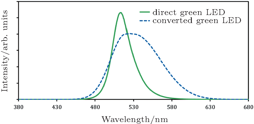
The disadvantage of converted green LEDs is the poor color purity. In Fig. 4, spectra of a direct GaN-based green LED and a phosphor-converted green LED are compared. Obviously, the phosphor converted green LED has a much broader spectrum, the typical full width at half maximum (FWHM) for direct GaN-based green LEDs is 30 nm– 35 nm, while the value for converted green LEDs is larger than 50 nm. In general, phosphor converted green LEDs can be used in white lighting, but it is not suitable for those applications requiring high purity green light.
2.2. Improving QW quality using AlGaN interlayerHigh indium content in green LEDs greatly impacts the quality of the InGaN QW. It may introduce new defects in the QW due to the large lattice mismatch between InGaN and GaN; it may cause phase separation or indium segregation due to limited intersolubility between InGaN and GaN; and it may result in a rough surface as the required growth temperature is low. These impacts are negative to the efficiency of green LEDs. Many methods were employed to improve the QW quality in aspects of material growth, such as increasing growth temperature, decreasing growth rate, etc.
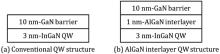
Nunoue[3, 20– 23] and his groups introduced a new QW structure that greatly enhanced the efficiency of green LEDs. A conventional QW consists of an InGaN quantum well and a GaN barrier. They inserted an AlGaN layer between the QW and barrier. As shown in Fig. 5, a QW structure consists of a 3-nm-thick InGaN QW layer, a 1-nm-thick AlGaN interlayer, and a 10-nm-thick InGaN barrier layer. With this structure, the authors achieved an EQE as high as 24.7% at 559-nm wavelength, which was a remarkable result.
The authors suggested that the AlGaN interlayer can suppress the generation of new dislocations, reduce indium content fluctuation, and smooth the surface, which results in an abrupt interface. With 90% Al in the interlayer, the authors even successfully grew InGaN-based red LED, whose EQE was 2.7% with a wavelength of 629 nm. Besides, the potential of AlGaN is much higher than that of InGaN, which provides a better carrier confining effect, but it also increases the difficulty of carrier transportation. Consequently, green LEDs with an AlGaN interlayer have a high operating voltage. Therefore, it is hard to say whether the AlGaN interlayer structure is a reasonable structure, as it has a high EQE but a low wall plug efficiency (WPE).
2.3. Strain engineering of QWTo improve the efficiency of green LEDs, another approach is to reduce the strain in QW. Strain not only influences device properties, but also affects epitaxial growth. A common method is to grow “ prestrained layers” before the QWs. The prestrained layers consist of InGaN layers, which can partially compensate strain for the subsequent QWs.
The indium content in a prestrained layer should be kept at a proper degree: too low has no strain compensation effect while too high may affect the crystal quality and absorb the light emitted from QWs. Blue LEDs usually use In0.05Ga0.95N/GaN superlattices as prestrained layers and green LEDs often choose In0.15Ga0.85N/GaN blue QWs as prestrained layers.
Yang[24– 27] and his group researched the prestrained layers intensively. They observed that with prestrained layers, more indium can be incorporated in the QWs, and thus the QWs can be grown at a higher temperature with a better quality. They also found that wavelength shift is smaller for the LEDs with prestrained layers, indicating a smaller piezoelectric field. XRD measurements were carried out to study the strain state within the QWs. Reciprocal space mappings (RSM) of (105) reflection for a sample with prestrained layers and a sample without prestrained layers, were scanned by high resolution XRD. The InGaN QW of the sample without prestrained layers was fully strained, whereas the QW of the sample with prestrained layers was partially relaxed. Therefore it can be concluded that the prestrained layers can help to reduce strain for QWs.
Other strain engineering techniques were also developed, such as AlGaInN lattice-matched barrier, triangular QW, thin barriers, etc. Among these, the prestrain technology is most practical, as it can be easily realized in epitaxial growth. Most of today’ s commercial LEDs have prestrained layers within the structure.
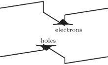
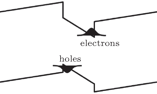
2.4. Reduction of polarization effect on semipolar GaNThe high piezoelectric field that exists in the QW of green LEDs brings the quantum confined Stark effect (QCSE), which causes band bending in the QW, resulting in carrier delocalization and electron overflow. As shown in Fig. 6, in the bent QW, electrons and holes tend to move toward their potential minimum, and the wave functions separate, which results in a low recombination rate and carrier accumulation. The accumulated carriers in the QWs will fill higher energy levels, making it easier for the electrons to escape from the QW. Moreover, downward bending of QW reduces the effective potential height of the barrier, which also increases the probability of electron overflow.
Although strain can be partially relaxed as discussed in Subsection 2.3, the piezoelectric field in the QW is still very large. A concept of nonpolar QW was proposed, which means to grow QWs in the directions without polarization effect. The QCSE would be reduced without a piezoelectric field, while the wave function overlapping of electrons and holes would be enhanced.
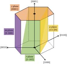
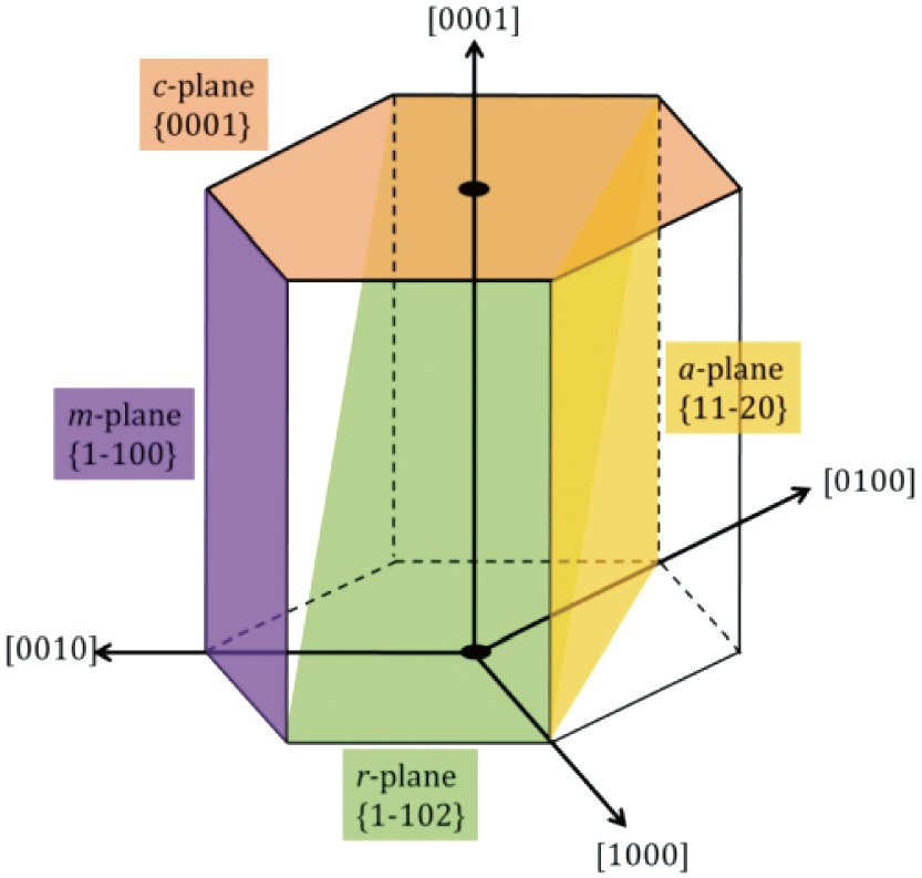
Normally, the (0001) plane (c-plane) is most common in GaN growth, the planes perpendicular to the c-plane such as (1-100) (m-plane) and (11-20) (a-plane) planes, are nonpolar planes, as shown in Fig. 7. GaN grown on these planes would have no polarization field in the QW. The idea is excellent, but it is challenging for material growth. First, the acquisition of nonpolar substrates is quite hard, a-plane GaN can be grown on r-plane sapphire or a-plane GaN, and m-plane GaN can be grown on (10-10) LiAlO2 or m-plane GaN. Second, it is difficult to grow high quality nonpolar GaN with a smooth surface. The stacking fault defects density is very high in nonpolar GaN. And the indium incorporation efficiency is not as high as c-plane InGaN. Much research on nonpolar green LED has been reported, [28– 31] but the results did not meet expectations.
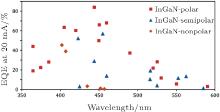
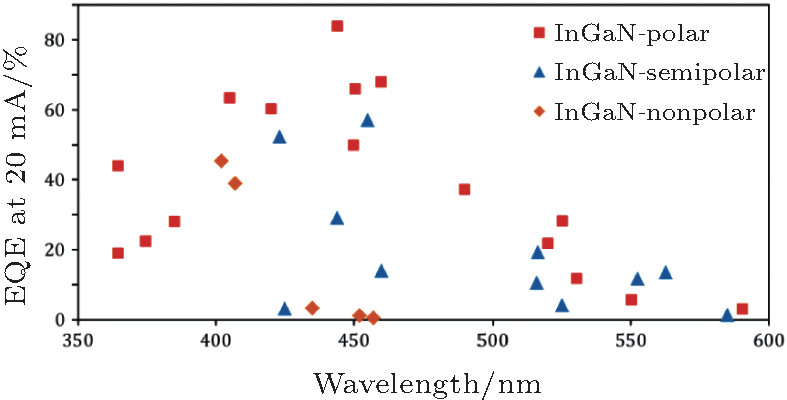
The planes obliquely crossed by the c-plane are semipolar planes. There are many semipolar planes, such as (10-11), (10-1-1), (20-21), (10-13), and (11-22). Again, the biggest problem for semipolar LEDs is the material growth. Many results of semipolar green LEDs have been reported, [32– 40] which are plotted in Fig. 8, accompanied by the results of nonpolar and polar LEDs. One can observe that the polar LEDs have the best performance overall. The efficiency of nonpolar and semipolar LEDs did not meet expectations, which was mainly attributed to the difficulty of material growth.
3. Development of highly efficient high power GaN green LEDs on Si substrate3.1. The advantages of Si substrateSapphire is the most common substrate for current commercialized LEDs, while Si and SiC substrate LEDs have also been industrialized. Growing GaN LEDs on Si is challenging work because the lattice mismatch and thermal mismatch between GaN and Si are both large, but there are also many advantages.
Concerning heat conductivity, the self-heating effect is more serious in green LEDs, as they are less efficient than blue LEDs; thus heat transfer is an important issue for green LEDs. Sapphire substrate has low thermal conductivity, resulting in high junction temperature. The rising temperature may greatly affect the performance of LEDs. However, fortunately, Si has high thermal conductivity, which could be the right choice.
Besides, LEDs with Si substrates can be easily processed into a vertical thin film structure (VTF). VTF-LEDs have high light extraction efficiency, good current spreading, and less side emission, which together make them a high quality light source candidate.
Moreover, both lattice mismatch and thermal mismatch between GaN and Si generate tensile strain in GaN, which is beneficial for QW growth and device performance. With the same emission wavelength, the QW growth temperature of LEDs on Si substrate can be set 20 degrees higher than that of sapphire, which is helpful for improving the quality of QWs. The as-grown GaN film under tensile strain can compensate the compressive strain in the QWs, which also benefits the performance of green LEDs.
In summary, developing green LEDs on Si substrate is an attractive topic. We have indeed done comprehensive research on it, and successfully obtained top level green LEDs on Si substrate.
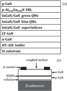
The epitaxial basic structure is illustrated in Fig. 9. It starts from a 100-nm-thick high temperature (HT) AlN buffer layer, and then grows a 2.4-μ m-thick Si-doped n-GaN. After that, prestrained layers with a low temperature (LT) GaN layer, 10 periods of InGaN/GaN superlattices and 6 periods of InGaN/GaN blue QWs are grown, the active region formed by seven periods of InGaN/GaN green QWs followed by an AlGaN electron blocking layer (EBL). Finally, p-GaN is grown to complete the structure.
The as-grown wafers are processed into VTF-LED chips. As shown in Fig. 9(b), the epitaxial layers are bonded on a conductive Si submount with Ag as a reflector, and the top surface is roughed by wet etching — these can both improve light extraction efficiency. The electrodes are vertically aligned, which is beneficial for current spreading.[41, 42]
Based on the structures introduced above, the following sections will focus on our research into green LEDs on a Si substrate. Several experiments were carried out from different aspects to improve the performance of green LEDs on Si substrate.
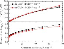
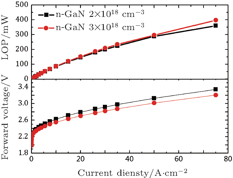
3.2. Effects of n-GaN doping concentration on device properties of green LEDsDoping concentration of Si in n-GaN is an important issue, as it can influence carrier transport in LEDs. A high carrier concentration in n-GaN leads to low serial resistance and better current spreading, but it may also result in worse crystal quality and GaN film cracking. Two samples with the same structure but different doping level in n-GaN were grown on Si substrate, the Si concentrations of n-GaN for the two samples were 2× 1018 cm− 3 and 3× 1018 cm− 3, respectively. Rocking curves of (002) and (102) planes were scanned to evaluate the crystal quality of two samples, and lattice parameters were measured by high resolution XRD.
With 2× 1018 cm− 3 Si doping in n-GaN, FWHM of (002) and (102) rocking curves are 345 arcsec and 355 arcsec, respectively. It can be said that the GaN film has a good crystal quality as total thickness of the LED structure is only 3 μ m. When increasing Si concentration to 3× 1018 cm− 3, FWHMs of (002) and (102) rocking curves increase to 370 arcsec and 380 arcsec, respectively. This means that the crystal quality of GaN become worse as the doping concentration of n-GaN increased. Normally, Si substitutes Ga in the lattice. As the radius of Si atoms is smaller than that of Ga atoms, more Si will lead to a smaller a-axis lattice parameter.
Table 1.
Table 1.
 Table 1. FWHMs and lattice parameters of samples with different n-doping concentrations.| Si concentration | FWHM of (002), (102) | Lattice parameters a, c |
|---|
| 2× 1018 cm− 3 | 345 arcsec, 355 arcsec | 3.1930 Å , 5.1825 Å | | 3× 1018 cm− 3 | 370 arcsec, 380 arcsec | 3.1928 Å , 5.1826 Å |
| Table 1. FWHMs and lattice parameters of samples with different n-doping concentrations. |
The two samples were fabricated into VTF-LEDs with the same structure. Device properties of the LEDs were tested. Figure 10 plots the light output powers (LOP) and forward voltages under different current densities. With increasing Si doping concentration in n-GaN, the LOP was slightly enhanced by 1%, which may be attributed to better current spreading of higher n-GaN doping; the forward voltage was significantly reduced by 3%, which was mainly due to lower serial resistance with higher n-doping concentration.
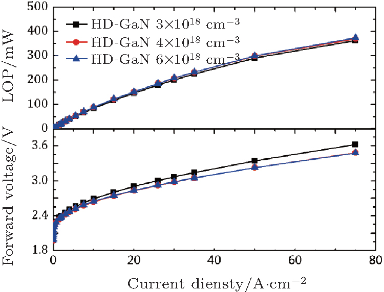
Totally, 4% efficiency was enhanced by increasing n-doping concentration from 2× 1018 cm− 3 to 3× 1018 cm− 3. But further increasing Si concentration may result in GaN film cracking and worse crystal quality. Therefore, a new n-GaN structure was designed which consists of a 2.1-μ m-thick normal-doped layer (3× 1018 cm− 3 Si) and a 0.3-μ m-thick heavily doped (HD) layer. The normal-doped layer can keep the crystal quality at a reasonable level and prevent film cracking, while the heavily doped layer was intended to provide high electron concentration. Three different doping concentrations of HD-GaN were compared, which were 3× 10¹⁸, 4× 10¹⁸, and 6× 1018 cm− 3 respectively. The devices’ results are plotted in Fig. 11. With increasing Si concentration in HD-GaN, the LOP did not change much, and the forward voltage dropped when Si concentration was increased to 4× 1018 cm− 3, but there was no further change when Si concentration was further increased to 6× 1018 cm− 3. Therefore, the optimal HD-GaN doping concentration was set to be 4× 1018 cm− 3.
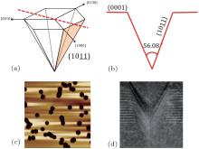
3.3. QW strain engineeringThe prestrained layers consist of an LT-GaN layer, 10 periods of InGaN/GaN SLs, and 6 periods of blue QWs. Each layer has its own function. The purpose of growing LT-GaN is to generate V-pits. A V-pit is a type of spatial defect with a cross section that looks like a “ V, ” as described in Fig. 12. Normally, a V-pit originates from a dislocation. Under certain growth conditions, the growth rate of GaN in the  direction can be much smaller than that in the [0001] direction, which forms a hexagonal pyramid-shaped pit. As the film grows thicker, the size of V-pits becomes larger.
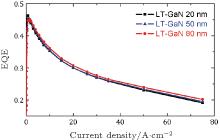
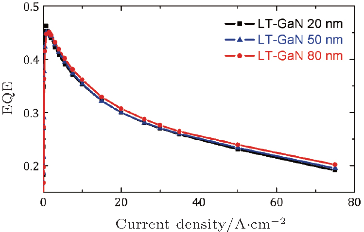
V-pits have many functions, one of which is relaxing strain. The V-pits can split the QW from a single large area into small parts, stop stress propagation, and turn long range stress into localized stress, which can effectively reduce the stress in QWs. V-pits can also passivate dislocations to reduce the non-radiative recombination rate. The slower growth rate of V-pits’ sidewalls leads to thinner QWs with less indium content on the sidewalls. The potential near sidewalls will be higher than that of c-plane QWs, thus fewer carriers will recombine near dislocations. The V-pits may also benefit hole injection, as holes can transport through the side walls into the QWs.[43, 44] Three LED samples with different LT-GaN thicknesses, 20 nm, 50 nm, and 80 nm, respectively, were grown to investigate the effects of V-pits’ size on the efficiency of green LEDs. A thicker LT-GaN layer indicated a larger V-pit size. EQEs of the three samples were plotted in Fig. 13. It is observed that the EQE increases with increasing LT-GaN thickness, implying that larger V-pits are preferred in green LEDs.
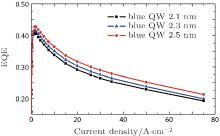
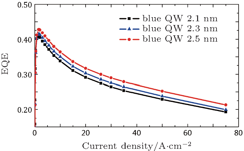
The prestrained blue QWs are crucial to relax strain for the green QWs. (The reasons have been discussed in Subsection 2.3.) There is a significant difference in efficiency between the LEDs with and without blue QWs as prestrain layers. In this section, the impact of blue QWs’ thickness on the efficiency of a green LED is studied. Three green LED samples with different blue QWs were grown on Si substrate, the blue QW thicknesses of the three samples were 2.1, 2.3, and 2.5 nm, respectively. As shown in Fig. 14, the EQE of green LEDs increases with increasing thickness of blue QWs in the prestrained layers. More indium can be incorporated in a thicker blue QW, so more strain can be relaxed. Therefore, the green LED with the thickest blue QW has the highest EQE.
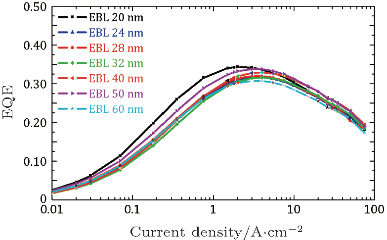
3.4. Thickness of EBLThe EBL is a very common structure in GaN-based LEDs, as it can effectively suppress electrons overflowing from QWs. In green LEDs, the piezoelectric field is much larger than that in blue LEDs, resulting in more severe current leakage. Hence the EBL layer should be redesigned to provide a better electron blocking effect. An experiment was done to investigate the impacts of EBL thickness on the efficiency of green LEDs. Seven green LEDs with EBL thicknesses from 20 nm to 60 nm were grown on Si substrate, the Al content of EBL was fixed at 20%. EQEs of the samples are plotted in Fig. 15. At low current density, the sample with the thinnest EBL has the highest efficiency. At high current density, the sample with the highest EQE has an EBL thickness of 50 nm.
The EBL can suppress electrons overflowing, which favors efficiency, but it also increases hole injection difficulty, negatively impacting efficiency. At low current density when electron overflow is not severe, the EBL has only a negative impact on hole injection; thus the sample with the thinnest EBL has the highest efficiency. At high current density, the positive impact of electron blocking is dominant when EBL thickness is less than 50 nm; but the negative impact on hole injection becomes dominant when EBL thickness is increased to 60 nm. Therefore, the optimal EBL thickness for green LEDs is set to be 50 nm.
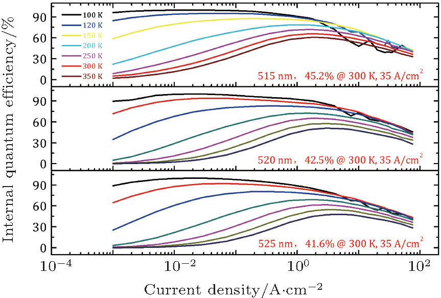
3.5. Toward longer wavelength and higher efficiencyThe development of GaN-based green LEDs on Si substrate is challenging work that needs systematic research on every aspect. Above, we introduced some representative techniques. There are many other techniques of material growth, structure design, and chip fabrication, omitted due to page limitation. By integrating these techniques together, we have successfully obtained high quality, high efficiency, high power green LEDs on Si substrate, which are already commercially available. Figure 16 plots the IQE curves of green LEDs with different wavelengths under different temperatures. At 35 A/cm2 and room temperature, the green LEDs with 515-, 520-, and 525-nm wavelength achieve IQE of 45.2%, 42.5%, and 41.6%, respectively, which are of the same level with the best results on sapphire and SiC substrates. In the longer wavelength range up to 566 nm, high power yellow LEDs with 9.4% EQE have been grown on Si substrate, [45] which is competitive with AlGaInP yellow LEDs. With further improvement and optimization, it is believed that the GaN-based LEDs on Si substrate should have a bright future in the green spectral region.


 , Wang Guang-Xu, Mo Chun-Lan, Xu Long-Quan, Ding Jie, Quan Zhi-Jue, Wang Xiao-Lan, Pan Shuan, Zheng Chang-Da, Wu Xiao-Ming, Fang Wen-Qing, Jiang Feng-Yi]