


Finite size effects on the quantum spin Hall state in HgTe quantum wells under two different types of boundary conditions*
[Cheng Zhi, Chen Rui, Zhou Bin† ]
]
]
|
|


†Corresponding author. E-mail: binzhou@hubu.edu.cn
*Project supported by the National Natural Science Foundation of China (Grant No. 11274102), the Program for New Century Excellent Talents in University of the Ministry of Education of China (Grant No. NCET-11-0960), and the Specialized Research Fund for the Doctoral Program of Higher Education of China (Grant No. 20134208110001).
The finite size effect in a two-dimensional topological insulator can induce an energy gap Eg in the spectrum of helical edge states for a strip of finite width. In a recent work, it has been found that when the spin–orbit coupling due to bulk-inversion asymmetry is taken into account, the energy gap Eg of the edge states features an oscillating exponential decay as a function of the strip width of the inverted HgTe quantum well. In this paper, we investigate the effects of the interface between a topological insulator and a normal insulator on the finite size effect in the HgTe quantum well by means of the numerical diagonalization method. Two different types of boundary conditions, i.e., the symmetric and asymmetric geometries, are considered. It is found that due to the existence of the interface between topological insulator and normal insulator this oscillatory pattern on the exponential decay induced by bulk-inversion asymmetry is modulated by the width of normal insulator regions. With the variation of the width of normal insulator regions, the shift of the Dirac point of the edge states in the spectrum and the energy gap Eg closing point in the oscillatory pattern can occur. Additionally, the effect of the spin–orbit coupling due to structure-inversion asymmetry on the finite size effects is also investigated.
The quantum spin Hall (QSH) effect is a band insulator with topological properties of electrons distinct from the normal insulator (NI). In a QSH system, there are topological protected gapless helical edge states with different spins moving in opposite directions in the bulk energy gap.[1, 2] Due to the protection of time reversal symmetry, the currents carried by the helical edge states are dissipationless and immune to nonmagnetic scattering. This kind of novel topological state of matter is also now called the two-dimensional topological insulator (TI). The first theory model on the QSH effect can be traced back to the works by Kane and Mele in 2005.[3, 4] In the Kane and Mele model of a graphene system, the intrinsic spin– orbit coupling (SOC) plays a key role in giving rise to the QSH effect. While later it was recognized that the intrinsic SOC strength in graphene is too weak for the topological protection to be relevant, [5] the Kane and Mele model captures the essential physics of the two-dimensional TI with nontrivial band topology and is still extensively used in theoretical study of the QSH effect.[6– 9] In 2006, a more realistic model for the QSH effect was proposed by Bernevig, Hughes, and Zhang (BHZ) based on semiconductor HgTe/CdTe quantum well (QW).[10] Soon after, the theoretical prediction of the QSH effect in an inverted HgTe QW was confirmed by experiment with the observation of ballistic edge channels.[11] As the most popular example of two-dimensional TI, the QSH effect of the HgTe QW is a very active field of condensed matter physics. Recently, many groups have devoted considerable efforts to the theoretical and experimental study of the QSH state in the HgTe QW, inspired by the potential applications of the QSH effect for spintronic devices.[12– 25]
When the thickness d of the HgTe/CdTe QW is varied through a critical thickness dc (= 6.3 nm), the transition of electronic band structure from a normal to an “ inverted” type occurs, i.e., the case of d < dc corresponding to the NI and the case of d > dc to the TI.[10] According to the BHZ model, the mass or gap parameter M of the model changes its sign when the above-mentioned topological quantum phase transition from the normal to the topological insulating phase takes place. In most theoretical works, the helical edge states in the QSH effect are generally obtained by considering hard-wall boundary conditions in which the wave function vanishes at the interface between a TI and a vacuum. In a recent work, Michetti et al. solved the edge states of an HgTe/CdTe QW-based TI described by the BHZ model with soft-wall boundary conditions, [26] where the wave function does not vanish at the interface between TI and NI. It was shown that the density profile of the edge state bound to the interface is qualitatively affected by the soft-wall boundary conditions, which allows it to extend into both the TI and the NI regions. At a boundary between a TI and an NI, the Dirac point of the edge states appearing at the interface strongly depends on the ratio between the mass parameters M in the two regions.[26] It is interesting to note that the observation of Dirac electron states formed at the heterointerface between a TI and a conventional semiconductor was reported recently.[27] It was claimed that the successful formation of robust non-trivial edge channels at a solid-state interface is an essential step towards functional junctions based on TIs.[27– 30]
Zhou et al. has indicated that the finite size effect in two-dimensional TIs can couple the edge states on the two sides of the sample to induce an energy gap Eg in the spectrum of helical edge states for a strip of finite width L.[31] The theoretical result showed that the gap Eg due to the finite size effect should be 0.45 meV around L ≃ 200 nm in the QSH effect of HgTe/CdTe QWs, which has been verified experimentally.[32] In a recent work, Cheng and Zhou investigated the effects of the SOC due to bulk- and structure-inversion asymmetries on the finite size effect in HgTe QWs.[33] When the bulk-inversion asymmetry (BIA) is taken into account, it is shown that the energy gap Eg of the edge states due to the finite-size effect features an oscillating exponential decay as a function of the strip width of HgTe QWs.[33, 34] Furthermore, if the bulk- and structure-inversion asymmetries are considered simultaneously, the structure-inversion asymmetry (SIA) will induce the shifting of the energy gap Eg closing point.[33] BIA is determined by the HgTe QW structure itself, whereas SIA depends on internal and external electric fields of the material. Several recent theoretical works have noticed the importance of BIA and SIA on the physical properties of HgTe QWs.[35– 44] In the work by Cheng and Zhou, the boundary of a strip of the HgTe/CdTe QW is in fact assumed to be the interface between a TI and a vacuum.[33]
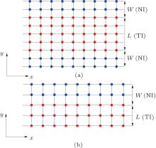
In this paper, we will investigate the effects of the solid-state interface, i.e., the interface between the TI and the NI regions, on the finite-size effect in the HgTe QW with BIA and SIA by means of the numerical diagonalization method. Two different types of boundary conditions are considered, i.e., the symmetric and asymmetric geometries. In the symmetric case, a TI strip is sandwiched between two NI strips with the same material parameters (Fig. 1(a)). In the asymmetric one, one side of the TI strip is a TI/NI interface, and the other side is a vacuum/TI interface (Fig. 1(b)). It is found that the oscillatory pattern on the exponential decay induced by BIA is modulated by the width of NI regions. With the variation of the width of NI regions, the shift of the Dirac point of the edge states in the spectrum and the energy gap Eg closing point in the oscillatory pattern can occur. Furthermore, the effect of SIA on the finite size effects is also investigated.
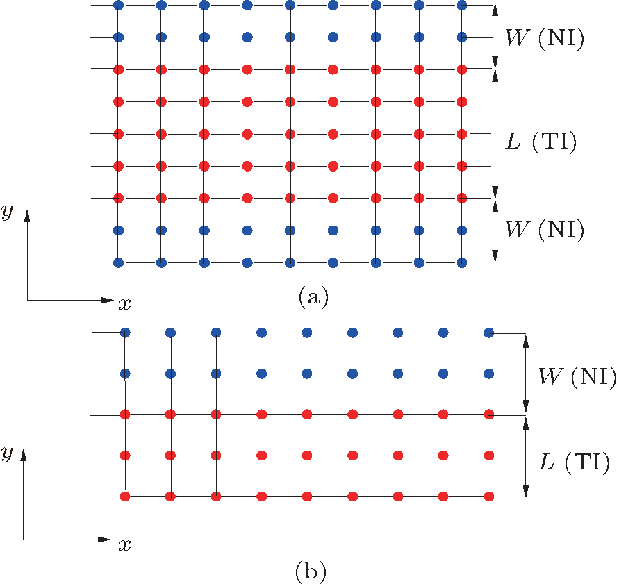 | Fig. 1. Schemes of the strip samples of two-dimensional TI under two different types of boundary conditions simulated by a tight-binding lattice. (a) The symmetric geometry: a TI strip is sandwiched between two NI strips with the same material parameters; (b) the asymmetric geometry: one side of the TI strip is a TI/NI interface, and the other side is a vacuum/TI interface. The TI region is a strip of an inverted HgTe QW with finite width L, and the NI region with width W is HgTe QW with a normal electronic band structure. In the text, the mass parameter M in the TI region is taken as − 10 meV, and in NI it is 10 meV. The lattice constant of the tight-binding model is a (= 2 nm). |
We start with the BHZ model with BIA and SIA terms given by the following four-band effective Hamiltonian, [10, 11, 36]

where 
In this section, we obtain the energy spectrum by numerical diagonalization of the tight-binding lattice model of Hamiltonian (1). Firstly we focus on the boundary condition with the symmetric geometry (Fig. 1(a)).
In Fig. 2, we plot the energy spectra of the HgTe QW with a symmetric geometry, in which the width L of the TI strip region is fixed to be 1000 nm and the width W of the NI region varies. Here, the strengths R and Δ are also firstly assumed to be zero, thus spin splitting of the edge states in the energy spectra due to the SOC effect does not occur. Because the width L of the TI strip is large enough, the energy gap Eg of the edge states due to the finite-size effect vanishes, that is, the gapless helical edge states appear in the bulk energy gap. Figure 2(a) presents the energy spectrum with the width W of the NI region being 0 nm, in which the energy value Ed at the Dirac point of the edge state is – MD/B.[31] From Figs. 2(b), 2(c), and 2(d), it is seen that when the TI/NI interface is taken into account the Dirac point of the edge states in the spectrum drops with increasing W. The dependence of the position of Dirac point Ed on the width W of the NI region is shown in Fig. 3(a). When the width W increases from 0 nm to 60 nm, Ed decreases distinctly from 7.46 meV to 0.58 meV. The numerical results present that Ed eventually saturates at the value 0.37 meV with the width W further increasing. The localization length of the edge state of QSH effect is about 55 nm in the inverted HgTe QW.[31] Due to the existence of the TI/NI interface, edge states also decay into NI regions and the spatial distribution of edge states changes.[26] When the width W of the NI region is much larger than the localization length of the edge state, the effect of the variation of the width W on the edge state of the QSH effect can be neglected.
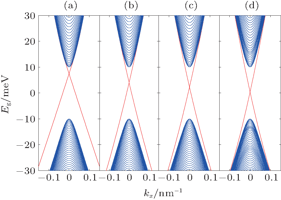 | Fig. 2. Energy spectra of the HgTe QW with a symmetric geometry. The width L of the TI region is 1000 nm, and the width W of the NI region is (a) W = 0 nm; (b) W = 10 nm; (c) W = 20 nm; (d) W = 100 nm, respectively. Here the strengths R and Δ are assumed to be zero. |
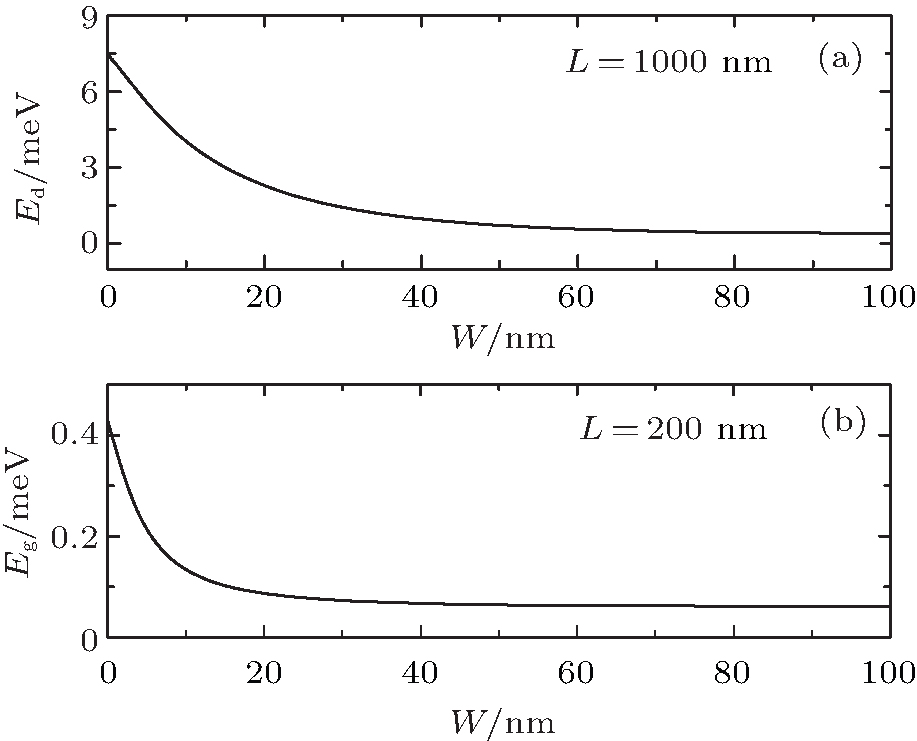 | Fig. 3. (a) The dependence of the position of Dirac point Ed on the width W of the NI region in a symmetry geometry, for the width L of the TI region being 1000 nm; (b) the dependence of energy gap Eg of the edge states due to the finite-size effect on the width W of the NI region in a symmetry geometry, for the width L being 200 nm. Here it is assumed that Δ = R = 0. |
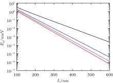
When the width L of a TI strip is finite, due to the finite size effect of QSH states, the energy gap Eg of the edge states will open. The dependence of energy gap Eg on the width W of the NI region in a symmetry geometry with the width L of the TI region being 200 nm is plotted in Fig. 3(b). It is observed that the energy gap Eg decreases as the width W increases and eventually saturates at about 0.06 meV. In Fig. 4, we plot the exponential decay of the energy gap Eg as a function of the TI strip width L for different width W of the NI region. The black line corresponds to the vacumm/TI interface (W = 0 nm), and the variations corresponding to the NT/TI interface with different W of 10 nm, 20 nm, and 100 nm are shown, respectively. With the width W increasing, the energy gap Eg is smaller and subjects to have a faster decay.
 | Fig. 4. The variation of the energy gap Eg with the width L of TI strip region for different width W of NI region in a symmetry geometry. The black line corresponds to the case of W = 0, the blue line to the width W = 10 nm, the purple line to the width W = 20 nm, and the red line to the width W = 100 nm. Here it is assumed that Δ = R = 0. |
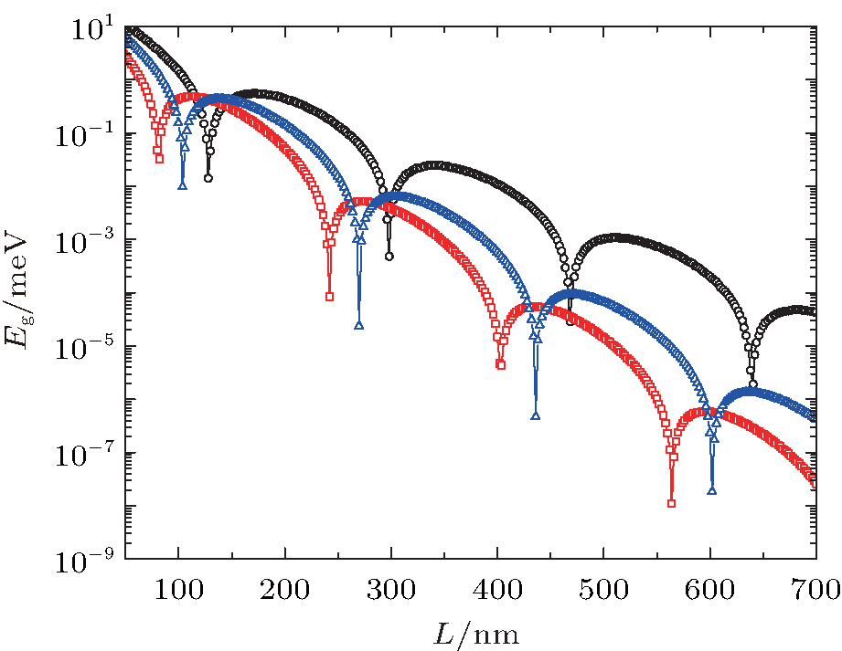
In the previous work, it has been found that when SOC due to BIA is taken into account, the energy gap Eg of the edge states features an oscillating exponential decay as a function of the strip width L of the inverted HgTe QW.[33, 34] Here, we adopt firstly the strength of BIA term Δ = 1.6 meV[35] and neglect the SIA term (i.e., R = 0). Numerical results show that this oscillatory pattern on the exponential decay induced by BIA is modulated by the width W of NI regions. In Fig. 5, we plot the variation of the energy gap Eg with the width L of the TI strip region for different width W of the NI region in a symmetry geometry. It is observed that with increasing the width W of the NI region the energy gap Eg firstly vanishes at a narrower width L of a TI strip. For instance, when W = 0 nm, 10 nm, 20 nm, and 100 nm, the energy gap Eg firstly closes nearly at L ≃ 392 nm, 356 nm, 342 nm, and 322 nm, respectively. Aiming to further find the effect of the width W on the oscillation period of this oscillatory pattern, in Fig. 6, we sightly overestimate the strength Δ of the BIA and take Δ = 6.4 meV. It is shown that with increasing W, the oscillation period of the energy gap Eg decreases. For W = 0 nm, 10 nm, and 100 nm, the oscillation period is about 170 nm, 166 nm, and 160 nm, respectively.
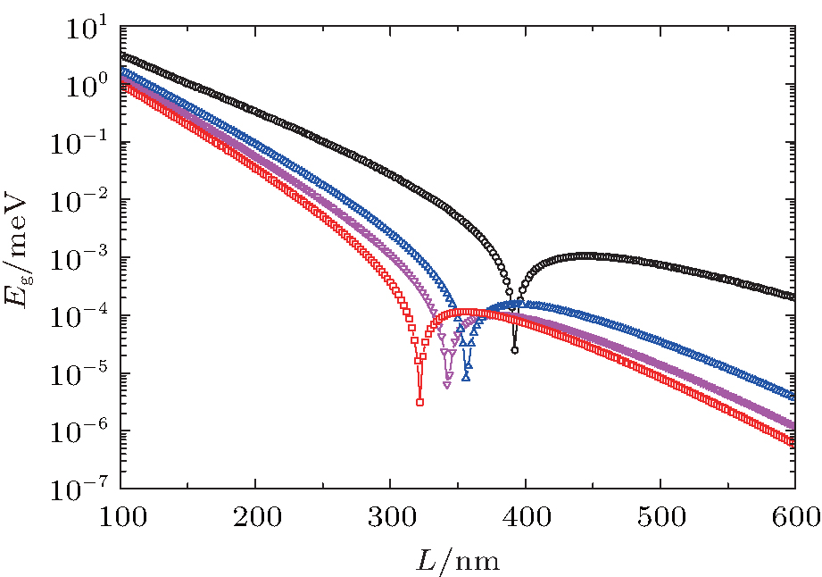 | Fig. 5. The variation of the energy gap Eg with the width L of the TI strip region for different width W of the NI region in a symmetry geometry. The black circle symbol corresponds to the case of W = 0, the blue triangle symbol to the width W = 10 nm, the purple inverted triangle symbol to the width W = 20 nm, and the red square symbol to the width W = 100 nm. Here it is assumed that Δ = 1.6 meV and R = 0. |
 | Fig. 6. The variation of the energy gap Eg with the width L of the TI strip region for different width W of the NI region in a symmetry geometry. The black circle symbol corresponds to the case of W = 0, the blue triangle symbol to the width W = 10 nm, and the red square symbol to the width W = 100 nm. Here it is assumed that Δ = 6.4 meV and R = 0. |
As mentioned above, the strength R of the SIA term can be tuned by a gate voltage. When the BIA and SIA terms are together taken into account, the size-dependence of the energy gap Eg for different strength R (R = 0, 80 meV· nm, and 160 meV· nm, respectively) and the strength Δ = 1.6 meV is shown in Fig. 7, where the width W of NI regions is taken as 100 nm. It is seen that due to the SIA, the energy gap Eg vanishes at a narrower width L of TI strip. For the case Δ = 1.6 meV, when R = 80 meV· nm and 160 meV· nm, the energy gap Eg vanishes at L ⋍ 258 nm and 174 nm, respectively. It is also found that with increasing R, the oscillation period of the energy gap Eg decreases.
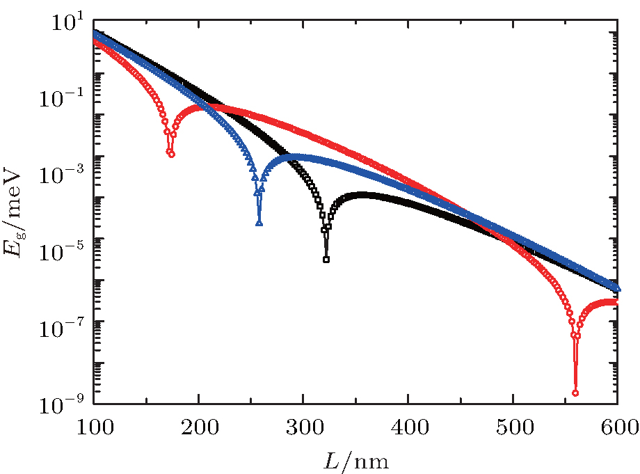 | Fig. 7. The variation of the energy gap Eg with the width L of the TI strip region for different strength R of the SIA term in a symmetry geometry. The black square symbol corresponds to the case of R = 0, the blue triangle symbol to the strength R = 80 meV· nm, and the red circle symbol to the strength R = 160 meV· nm. Here it is assumed that Δ = 1.6 meV and W = 100 nm. |
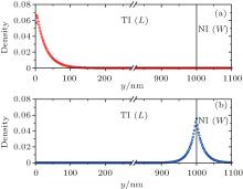
Now we proceed to study the case with an asymmetric geometry, in which one side of the TI strip is a TI/NI interface, and other side is a vacuum/TI interface (see Fig. 1(b)). In Fig. 8, we show the energy spectra of the HgTe QW with an asymmetric geometry, in which SOC due to BIA and SIA are neglected, the width L of the TI region is 1000 nm, and the width W of the NI region is 100 nm. As the two edges of the HgTe QW with an asymmetric geometry are not equivalent, the edge states are not degenerate. Therefore, two different Dirac points appear in the energy spectra and are indicated by the arrows 3 and 4, respectively, in Fig. 8. The Dirac point indicated by arrow 3 comes from the helical edge states along the vacuum/TI interface, and the Dirac point indicated by arrow 4 comes from the helical edge states along the TI/NI interface. The result can be confirmed by the density distributions of the edge states plotted in Fig. 9. In Fig. 9(a), the red circle symbol characterizes the density distribution of the spin-up edge state at the Dirac point indicated by the arrow 3, and figure 9(b) characterizes the density distribution of the spin-up edge state at the Dirac point indicated by arrow 4. Without SOC due to BAI and SAI, the density distributions of the spin-up and spin-down edge states at kx = 0 coincide completely with each other.
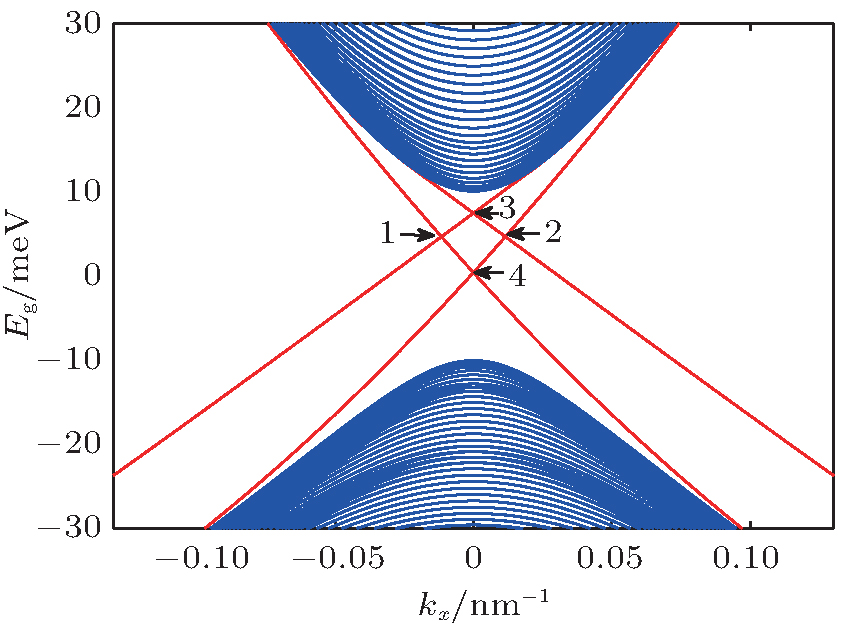 | Fig. 8. Energy spectra of the HgTe QW with an asymmetric geometry with one side of the TI strip being a TI/NI interface, and other side being a vacuum/TI interface (Fig. 1(b)). Here the strengths R and Δ are assumed to be zero, the width L of the TI region is 1000 nm, and the width W of the NI region is 100 nm. |
 | Fig. 9. Density distributions of the spin-up edge states in the HgTe QW with an asymmetric geometry at kx = 0. (a) The case corresponding to Dirac point indicted by arrow 3 in Fig. 8; (b) The case to Dirac point indicted by arrow 4. Here the strengths R and Δ are assumed to be zero, the width L of the TI region is 1000 nm, and the width W of the NI region is 100 nm. |
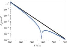
Note that in the asymmetric geometry when the width L of the TI strip is finite, the energy gap Eg of the edge states will generically open at this finite kx rather than at kx = 0. That is, due to the finite size effect of QSH states, the energy splitting occurs at points indicated by arrows 1 and 2 rather than Dirac points indicated by arrows 3 and 4 in the energy spectra of Fig. 8. In Fig. 10, we plot the exponential decay of the energy gap Eg as a function of the TI strip width L for the two cases without BIA and with the BIA strength Δ = 1.6 meV, respectively. By numerical calculation, when the width W of the NI region in the asymmetric geometry is 100 nm, the energy gap closes nearly at L = 386 nm for strength Δ = 1.6 meV and R = 0.
 | Fig. 10. The variation of the energy gap Eg with the width L of the TI strip region for different strength Δ of BIA term in an asymmetry geometry. The black square symbol corresponds to the case of Δ = 0, and the blue circle symbol to the strength Δ = 1.6 meV. Here it is assumed that R = 0 and W = 100 nm. |
In this paper, we focus on the effect of the TI/NI interface on finite-size effects on the QSH state in HgTe QWs, based on the tight-binding lattice model of the four-band BHZ model with BIA and SIA terms and by means of the numerical diagonalization method. Two different types of boundary conditions, i.e., the symmetric and asymmetric geometries, are considered respectively. It was found recently that when the BIA term is taken into account, the energy gap Eg of the edge states due to the finite-size effect features an oscillating exponential decay as a function of the strip width of the inverted HgTe QW with two sample vacuum/TI interfaces. Our numerical results present that due to the existence of the TI/NI interface this oscillatory pattern on the exponential decay induced by BIA is modulated by the width of NI regions. The Dirac point of the edge states in the spectrum drops with increasing the width W of NI regions, and eventually saturates with the width W further increasing. It is also observed that with the variation of the width of NI regions, the shift of the energy gap Eg closing point and the change of the oscillation period in the oscillatory pattern occur. When the BIA and SIA terms are together taken into account, with increasing the strength of the SIA term, the oscillation period of the energy gap Eg decreases. In the case of the asymmetric geometry boundary, there are two different Dirac points in the spectrum of the edge states. Furthermore, different from the case of the symmetric geometry, the energy gap of the edge states generically opens at this finite kx rather than at Dirac points (kx = 0). Our results about the effect of the TI/NI interface on finite-size effects may provide a new method to manipulate the edge states in feature applications of spintronic devices based on the HgTe QWs.
| 1 |
|
| 2 |
|
| 3 |
|
| 4 |
|
| 5 |
|
| 6 |
|
| 7 |
|
| 8 |
|
| 9 |
|
| 10 |
|
| 11 |
|
| 12 |
|
| 13 |
|
| 14 |
|
| 15 |
|
| 16 |
|
| 17 |
|
| 18 |
|
| 19 |
|
| 20 |
|
| 21 |
|
| 22 |
|
| 23 |
|
| 24 |
|
| 25 |
|
| 26 |
|
| 27 |
|
| 28 |
|
| 29 |
|
| 30 |
|
| 31 |
|
| 32 |
|
| 33 |
|
| 34 |
|
| 35 |
|
| 36 |
|
| 37 |
|
| 38 |
|
| 39 |
|
| 40 |
|
| 41 |
|
| 42 |
|
| 43 |
|
| 44 |
|