
Metal–organic–vapor phase epitaxy of InGaN quantum dots and their applications in light-emitting diodes*
[Wang Lai† , Yang Di, Hao Zhi-Biao, Luo Yi]
, Yang Di, Hao Zhi-Biao, Luo Yi]
|
|


†Corresponding author. E-mail: wanglai@tsinghua.edu.cn
*Project supported by the National Basic Research Program of China (Grant Nos. 2013CB632804, 2011CB301900, and 2012CB3155605), the National Natural Science Foundation of China (Grant Nos. 61176015, 61210014, 51002085, 61321004, 61307024, and 61176059), and the High Technology Research and Development Program of China (Grant No. 2012AA050601).
InGaN quantum dot is a promising optoelectronic material, which combines the advantages of low-dimensional and wide-gap semiconductors. The growth of InGaN quantum dots is still not mature, especially the growth by metal–organic–vapor phase epitaxy (MOVPE), which is challenge due to the lack of itin-situ monitoring tool. In this paper, we reviewed the development of InGaN quantum dot growth by MOVPE, including our work on growth of near-UV, green, and red InGaN quantum dots. In addition, we also introduced the applications of InGaN quantum dots on visible light emitting diodes.
In the 1980s and 1990s, Japanese scientists pioneered the invention of GaN-based blue light emitting diodes (LEDs), which were first commercialized by Nichia in 1992.[1– 4] Since then, research on III-nitride materials and devices has been growing worldwide. Up to now, the performance of blue LEDs is excellent enough to fabricate high lumen efficiency white LEDs. The external quantum efficiency of blue LEDs has surpassed 70%, while the internal quantum efficiency can even reach 90%. This means the quality of InGaN/GaN blue multi-quantum-wells (MQWs) is already very high, though the dislocation density is still around 108 cm− 3 in hetero-epitaxial GaN. Recently, researchers have started to pay attention to InGaN quantum dots (QDs). QDs were first proposed by Arakawa in 1982.[5] This is a zero-dimensional material, which has atom-like energy levels and island-like shapes. These unique properties make QDs suitable for many important applications, e.g., low-threshold laser diodes (LDs) and single photon sources.[6– 8] InGaN QDs bring the advantages of wide gap semiconductors to QDs, so they provide new possibilities to realize some novel devices compared to conventional QDs.[9– 11]
Like quantum wells, InGaN QDs can be grown by either metal– organic– vapor phase epitaxy (MOVPE) or molecular beam epitaxy (MBE). For III-nitride semiconductors, usually the quality grown by MOVPE is superior to that by MBE. But for InGaN QDs, growth by MBE is much easier since it has strong in-situ monitoring tools. Actually, the first green and red LDs based on InGaN QDs were demonstrated by MBE.[9, 10] However, MOVPE is more promising in mass production, though control of the growth is still very challenging. In this paper, we will review the recent progress on InGaN QDs grown by MOVPE and their applications, including critical thickness of InGaN grown on GaN, growth and characterization of InGaN QDs dots with different indium compositions, light emitting diodes based on InGaN QDs. In Section 2, we will analyze the critical thickness of InGaN when it is grown on GaN and point out the challenges in self-assembly of InGaN QDs. In Section 3, we will introduce methods of growing near-UV InGaN QDs by alternate admittance of group-III and group-V precursors. In Section 4, we will describe the work on the growth of green and red InGaN QDs, especially the growth interruption method. In Section 5, we show some examples of LEDs based on InGaN QDs. Finally, we summarize the article in Section 6.
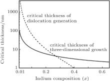
When InGaN is grown on GaN, compressive strain exists in InGaN due to the lattice mismatch between InGaN and GaN. The strain will accumulate as the thickness and indium composition of InGaN increase. When it exceeds a critical value, the strain will relax through two possible approaches, surface morphology transformation and dislocation generation.[12– 14] The former means InGaN is grown two-dimensionally (2D) first, and then 3-dimensionally (3D) when the thickness exceeds the critical thickness, which is called the Stranski– Krastanow (SK) mode, and the initial 2D layer is called the wetting layer. Most self-assembled growth of QDs is based on the SK mode. The critical thicknesses for surface morphology transformation and dislocation generation are different, but they were confused sometimes in previous publications.[15, 16] Zhao et al. calculated the critical thicknesses depending on the indium composition theoretically, as shown in Fig. 1.[14] They found that both kinds of critical thicknesses decrease with the increase of the indium content. When the indium content is less than 0.27, the critical thickness for 3D growth is smaller than that for dislocation generation, while when the indium content is more than 0.27, the situation is the opposite.
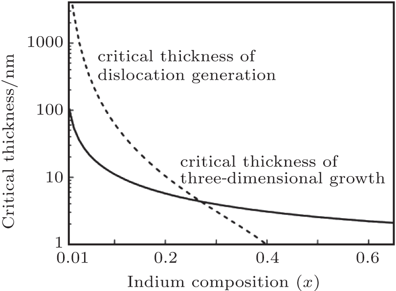 | Fig. 1. Critical thicknesses of InGaN grown on (0001) GaN for different strain relaxation: dislocation generation (dashed line) and three-dimensional growth (solid line). Reprinted from Ref. [12], Copyright 2011, with permission from Elsevier. |
These theoretical results also reflect the challenges for self-assembled growth of InGaN QDs. For low-indium-composition (less than 0.1) QDs, though the 3D growth occurs earlier than dislocation generation, the critical thickness is around 10 nm– 100 nm. This means the wetting layer is too thick if the QDs are grown by SK mode. For high-indium-composition (more than 0.3) QDs, the dislocation generation will occur earlier, which means that the SK mode growth does not work or there will be many dislocations in QDs even if it works. Note that GaN grown on sapphire substrates usually has a dislocation density of 108 cm− 2– 109 cm− 2. These dislocations will also influence the strain state in InGaN when it is grown on GaN. So the practical critical thickness would be a little larger than the calculated values. However, Pristovsek et al. found in their experiments that the wetting layer was thinner than Zhao’ s value when the indium composition was around 20%– 30%.[17]
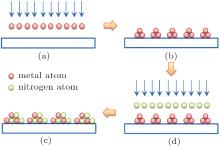
As discussed above, the low-indium-composition InGaN QDs are difficult to grow by SK mode since the wetting layer is too thick. This is very easy to understand. When the indium composition is low, the lattice mismatch between InGaN and GaN is small, so it needs enough thickness to accumulate the strain. In order to solve the problem, Zhao et al. grew the low-indium-composition by alternate admittance of group-III and group-V precursors instead of the conventional SK growth mode.[18] As shown in Fig. 2, in each period of alternate admittance of precursors, triethylgallium (TEGa), and trimethylindium (TMIn) were first injected without ammonia (NH3) for a few seconds, and then they were shut off and NH3 was injected for another few seconds. The principle of this method is very much like metal droplet epitaxy. Since the lattice mismatch between metal (In, Ga) and GaN is large enough, the metal islands are formed during the group-III precursor injection, and when NH3 is injected, the nitridation of metal islands will proceed to form InGaN QDs. On the other hand, volatilization of indium is strong during the growth, so the final indium content in InGaN QDs is low (∼ 4%).
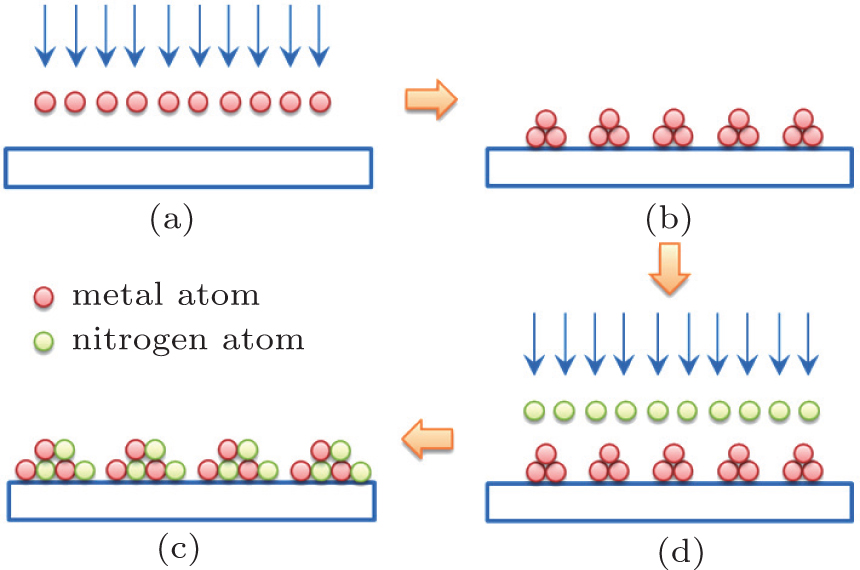 | Fig. 2. Schematic diagram of alternate admittance of precursors to form QDs: (a) metal precursors injection; (b) metal dots formation; (c) nitrogen precursors injection; (d) InGaN QDs formation. |
Figure 3(a) shows the typical surface morphology of InGaN QDs measured by atomic force microscopy (AFM). The density, diameter, and height of QDs are 2.3× 1010 cm− 2, 70 nm, and 2 nm, respectively. The photoluminescence (PL) spectrum at 10 K is shown in Fig. 3(b). The peak wavelength of QDs is 364 nm. The inset of Fig. 3(b) is the temperature-dependent PL peak wavelength and full width at half maximum (FWHM). The shift of peak wavelength is small and the FWHM increases with the temperature. These behaviors indicate there is no wetting layer beneath the QDs.
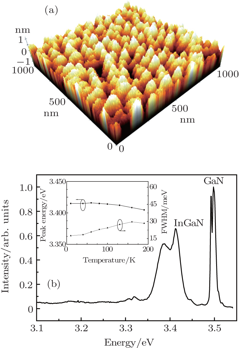 | Fig. 3. AFM image (a) and PL spectrum of low-indium-composition InGaN QDs. Reprinted from Ref. [18], Copyright 2012, with permission from Wiley. |
Green and red InGaN QDs with high indium composition are attractive because they promise to have better performance than InGaN quantum wells with the same emitting wavelength. The high-indium-composition InGaN quantum wells suffer from the quantum confined Stark effect (QCSE) induced by piezoelectric polarization.[19] But QDs can relax a part of the strain because of their 3D island-like shape.[20– 24] Therefore, the QCSE in QDs will be reduced.
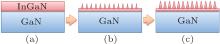
As discussed in Section 2, when the high-indium-composition InGaN QDs are grown on GaN directly, the dislocation generation will come before 3D growth. That means the traditional SK mode may not be suitable for green and red InGaN QDs growth. In 2003, Ji et al. first used a new method, a growth interruption method, to obtain blue InGaN QDs successfully.[25, 26] Then, the investigation of this method increased gradually.[27, 28] Zhao et al. studied the principle of the method and used it to grow both green and red InGaN QDs in 2011.[29] The growth interruption method usually includes two or three steps as shown in Fig. 4. First, a thin layer of InGaN is grown on GaN. Second, the group-III and group-V precursors are interrupted and only carrier gas is injected. During the interruption, the InGaN decomposes and some indium and gallium adatoms migrate on the surface to form 3D island-like InGaN dots. Third, another thin InGaN layer is deposited to adjust the size and density of QDs. If the morphology of formed QDs meets the requirements in the second step, the third step is no longer needed.
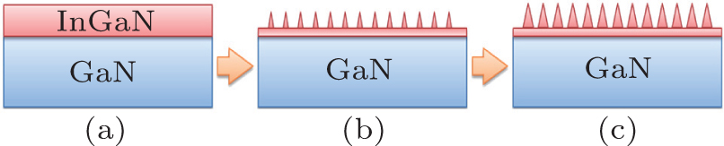 | Fig. 4. Schematic diagram of growth interruption method: (a) deposite InGaN film on GaN first; (b) growth interruption and adatoms migrate on the surface to form dots; (c) regrowth of InGaN to enlarge dots. |
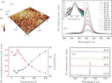
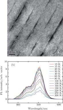
Wang et al. studied the influence of underlying GaN on the morphology of InGaN QDs.[30] QDs with a high aspect ratio were obtained. Figure 5 shows the typical morphology and the optical properties of high-indium-composition InGaN QDs with an aspect ratio of about 0.5 prepared by the growth interruption method. The diameter, height, and density of QDs are 14.3 nm, 7.6 nm, and 8× 109 cm2, respectively. Temperature-dependent PL spectra are shown in Fig. 5(b). The main peak around 490 nm corresponds to InGaN QDs, and the broad band around 400 nm– 440 nm under low temperature is believed to reflect the InGaN wetting layer. The normalized integral intensities and FWHM of the PL depending on temperature are plotted in Fig. 5(c). It is shown that as the temperature increases, the intensity first increases and then decreases, while the FWHM first decreases and then increases. These are typical behaviors of QDs that contain a wetting layer. All of this means that the growth interruption method is an SK growth mode in “ disguised” form. In addition, the sharp emission spectrum from a single QD is observed in low temperature micro-PL measurement, as shown in Fig. 5(d). The linewidth is about 0.036 nm, which is limited by the resolution of the instrument.
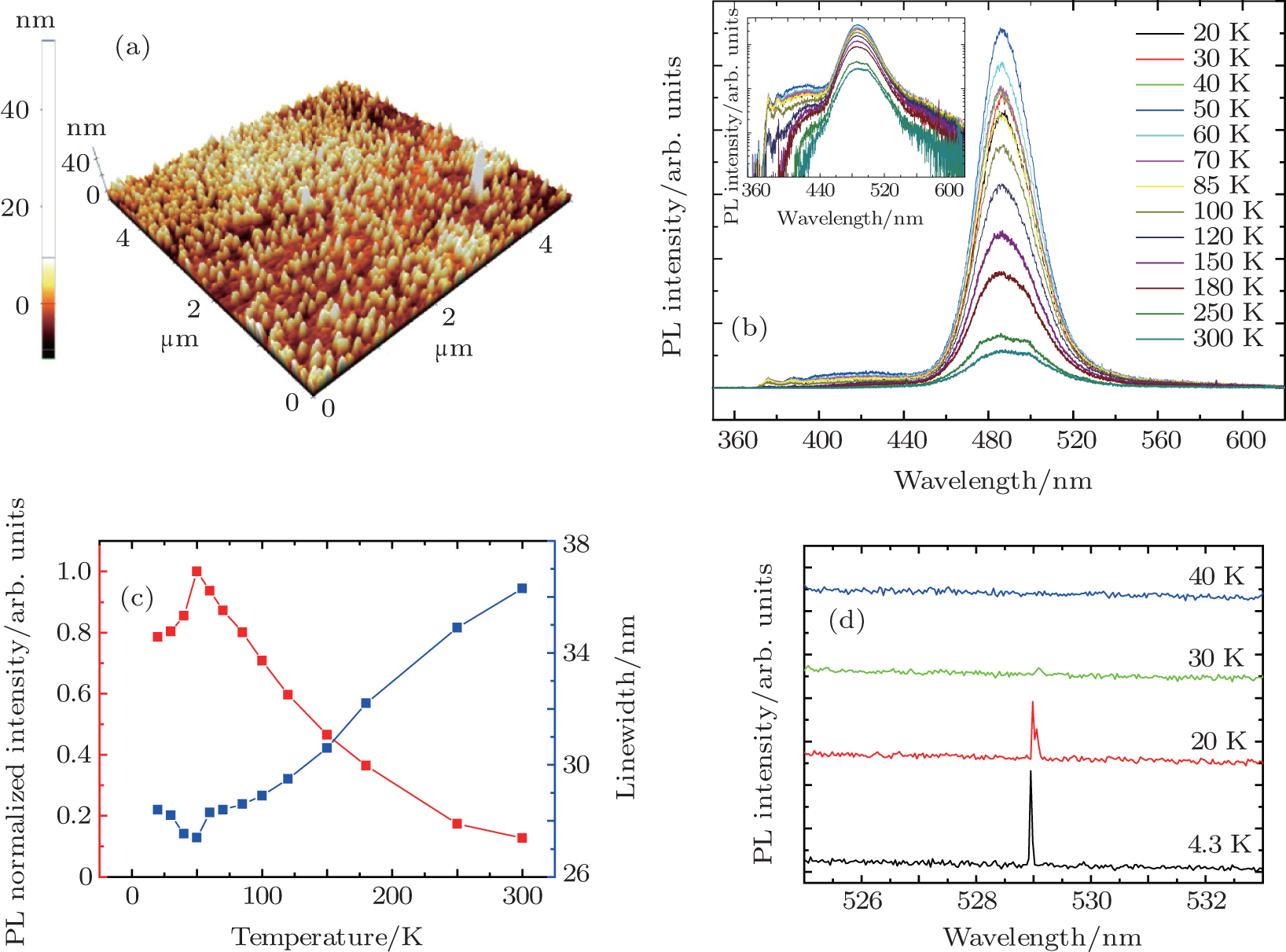 | Fig. 5. AFM image and optical spectra of InGaN QDs: (a) AFM image of InGaN; (b) temperature-dependent PL spectra, the inset in panel (b) is a plot of logarithmic vertical axis scale; (c) normalized intensity and FWHM under different temperatures; (d) micro-PL spectra of a single QD at low temperature. Reprinted from Ref. [30]. Copyright 2012, with permission from Wiley. |
The InGaN QDs can also be grown by other methods. For instance, Hommel et al. obtained the blue and green InGaN QDs by MOVPE using a phase-separation process based on spinodal and binodal decomposition.[31, 32] Park et al. realized the InGaN QDs from green to red by increasing the roughness of underlying GaN.[33]
Like the InGaN MQWs LED, the LED based on QDs also requires an active region of multi-layer InGaN/GaN QDs. Therefore, in order to fabricate the QDs LED, one must grow the multi-layer QDs material first. The key to the technique is obtaining the flat-surface GaN barrier on rough InGaN QDs for the growth of the next layer of QDs by MOVPE. Lü et al. investigated the growth process of GaN barrier systematically.[34] It was found that if the growth conditions of the GaN barrier were the same as those of InGaN QDs, for example, low temperature (650 ° C) and nitrogen carrier gas, the surface of the GaN barrier would be very rough. As a result, the morphology of the next-layer QDs was significantly different from that of previous ones.[35] To improve the quality of GaN, Lü et al. tried to increase the growth temperature and/or change the carrier gas to hydrogen and successfully got a flat surface of the GaN barrier, [34] as shown in Fig. 6(a). Based on the growth interruption method and optimized conditions of the GaN barrier, a 10-layer green QD sample with the radiative recombination efficiency of about 24% was realized, as shown in Fig. 6(b).
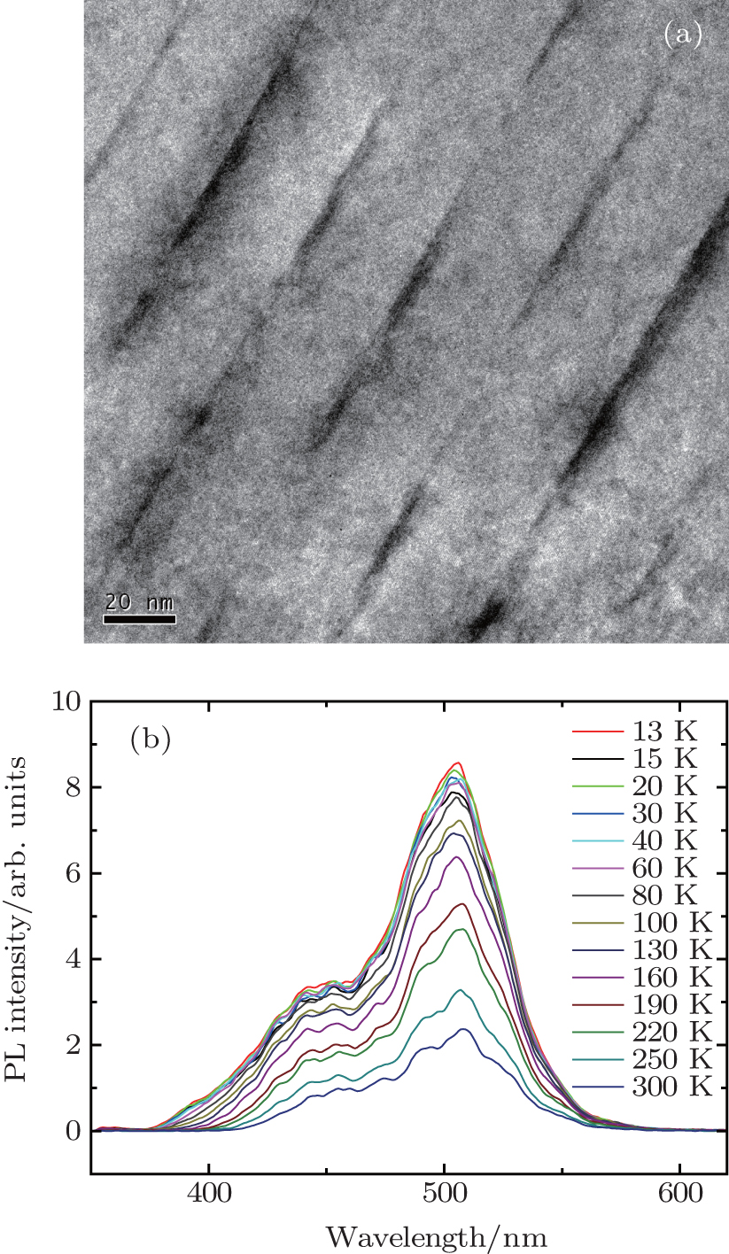 | Fig. 6. (a) Transmission electron microscopy image of 10-layer InGaN QDs; (b) temperature-dependent PL spectra of 10-layer InGaN QDs. The radiative recombination efficiency estimated by ratio of PL intensity at 300 K to 13 K is about 24%. Reprinted from Ref. [34]. |
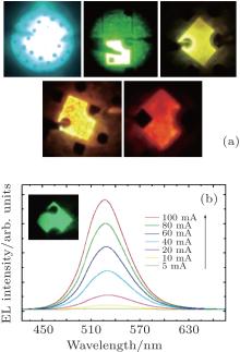
InGaN QDs LED can be grown by MOVPE based on a structure resembling conventional MQWs LEDs, except replacing the active region by multi-layer QDs. Through adjusting the growth temperature and the growth interruption process, the emitting wavelength can be well controlled from cyan to red, as shown in Fig. 7(a). Compared with MQWs LEDs, green and red LEDs based on QDs have wavelength-stability advantages when the injection current increases. For example, figure 7(b) shows the electroluminescence (EL) spectra of a green LED.[36] When the current density increases from 2 A/cm2 to 99 A/cm2, the peak wavelength shifts from 527.9 nm to 526.4 nm. This small blue shift of 1.5 nm means that the QCSE in the QDs is well suppressed. It is much smaller than that of c-plane MQWs LEDs, and better than previous results based on nano-structures, and can even be comparable with the best results in semipolar LEDs with the same wavelength. Longer-wavelength QDs LEDs were also demonstrated, and the blueshift was also smaller than that of the MQWs LEDs in the same wavelength range. Adding a superlattice structure underlying the multi-layer QDs is helpful to increase the indium incorporation and hence the emitting wavelength.[37] However, it has been observed that the dislocations increase dramatically in red QDs LEDs, and the current leakage in red QDs LEDs is also more severe than that in green ones.
 | Fig. 7. (a) Photos of QDs LEDs with different colors; (b) EL spectra depending on injection current. Reprinted from Ref. [36]. Copyright 2014, with permission from The Japan Society of Applied Physics. |
One interesting thing should be pointed out: the EL wavelength is abnormally 40-nm and 100-nm longer than the PL wavelength in InGaN green and red QDs LEDs, respectively.[36, 37] This observation is just the opposite of that in conventional c-plane MQWs LEDs. Nonuniformity of indium composition in different layers can be excluded by secondary ion mass spectroscopy (SIMS). This indicates that the carrier dynamics in PL and EL in InGaN QDs are very different, and it seems the unique behavior of high-indium-composition InGaN QDs, since some other publications reported similar results.[33, 38] The question is still open, and further study is needed.
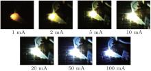
As the QDs exhibit advantages in emitting green to red light, it is promising to replace the yellow phosphors by QDs in current white LEDs. Actually, Chen et al. demonstrated the first phosphor-free white LEDs based on InGaN blue QWs and embedded yellow QDs.[39– 41] The solid solubility of InN in GaN is very low, so high-indium-composition InGaN easily forms phase separation. They utilized a strain-control method to enhance the phase separation and form QD-like indium-rich clusters in InGaN blue QW. Recently, our group also realized a phosphor-free white LED.[42] The active region included 4-period InGaN blue MQWs and 4-layer InGaN QDs grown by an interruption growth method. Actual pictures of the white LED under different injection currents are shown in Fig. 8. Though the color exhibits the obvious variation from yellow to blue as current increases, the color rendering index can be up to 62.
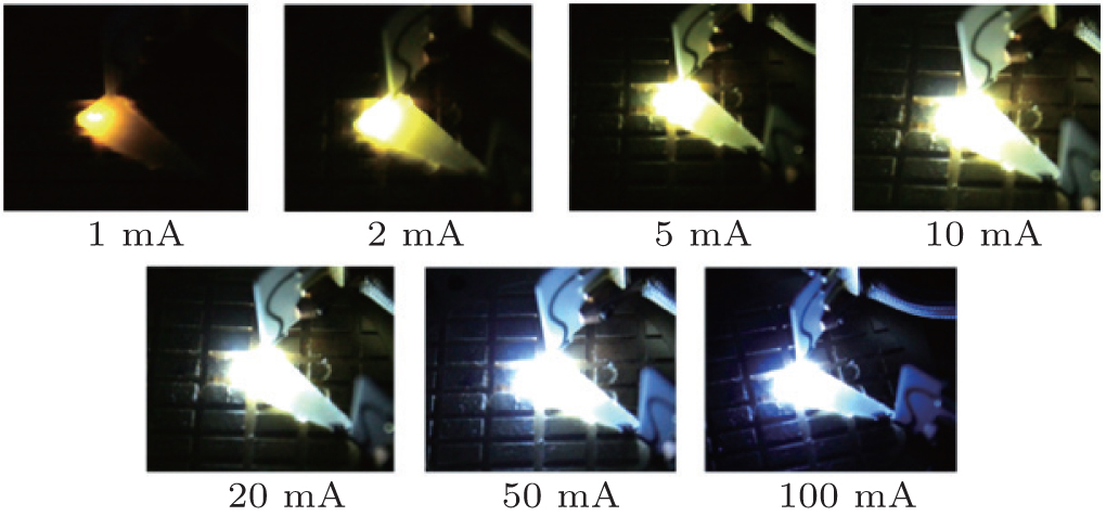 | Fig. 8. Photos of white LED under different injection current. At low current, the yellow QDs dominate the luminescence; while at high current, the blue QWs dominate the luminescence. Reprinted from Ref. [42], Copyright 2015, with permission from Elsevier. |
It should be clarified that the efficiency and the output light power of QDs LEDs are still much lower than those of QWs ones. For example, the typical light power of 530-nm green QDs LED is only about 1 mW at 20 mA estimated by our calibrated photodiode. The red and white QDs LEDs are much lower and cannot be detected by the photodiode. The low efficiency can be attributed to two origins. First, the density of QDs is not very high (typical value ∼ 109 cm− 2), so some of the carriers cannot be captured by the active region. Second, through TEM photos, it can be observed that there exist many dislocations at the interfaces between InGaN QDs and GaN barriers, though the lattices inside the QD are perfect. These dislocations will play a role on nonradiative recombination centers. In order to improve the efficiency and the output light power of QDs LEDs to meet the requirements of applications, there is still a long way to go to optimize the structure and growth quality of the QDs active region.
The recent progress on InGaN QDs growth has been reviewed in this paper. Theoretical study indicates the challenges for low- and high-indium-composition InGaN QDs growth. Near-UV InGaN QDs have been grown by alternate admittance of group-III and group-V precursors, while the growth interruption method has been introduced to the growth of green and red InGaN QDs. By optimizing the growth conditions of GaN barriers, multilayer QDs can be stacked well. As a result, green, red, and even white LEDs have been successfully demonstrated, respectively. These accomplishments exhibit the advantages of InGaN QDs on long visible wavelength emission. For the future, it is promising to realize the green low-threshold LD and high-color-rendering-index single chip white LED based on MOVPE-grown InGaN QDs. It is important to improve the quality of QDs further, including reducing the dislocations and increasing the density of QDs.
| 1 |
|
| 2 |
|
| 3 |
|
| 4 |
|
| 5 |
|
| 6 |
|
| 7 |
|
| 8 |
|
| 9 |
|
| 10 |
|
| 11 |
|
| 12 |
|
| 13 |
|
| 14 |
|
| 15 |
|
| 16 |
|
| 17 |
|
| 18 |
|
| 19 |
|
| 20 |
|
| 21 |
|
| 22 |
|
| 23 |
|
| 24 |
|
| 25 |
|
| 26 |
|
| 27 |
|
| 28 |
|
| 29 |
|
| 30 |
|
| 31 |
|
| 32 |
|
| 33 |
|
| 34 |
|
| 35 |
|
| 36 |
|
| 37 |
|
| 38 |
|
| 39 |
|
| 40 |
|
| 41 |
|
| 42 |
|