Effect of de-trapping on carrier transport process in semi-insulating CdZnTe*
[Guo Rong-Rong, Jie Wan-Qi† , Zha Gang-Qiang, Xu Ya-Dong, Feng Tao, Wang Tao, Du Zhuo-Tong]
, Zha Gang-Qiang, Xu Ya-Dong, Feng Tao, Wang Tao, Du Zhuo-Tong]
|
|


†Corresponding author. E-mail: jwq@nwpu.edu.cn
*Project supported by the National Instrumentation Program, China (Grant No. 2011YQ040082), the National Natural Science Foundation of China (Grant Nos. 61274081, 51372205, and 51202197), the National 973 Project of China (Grant No. 2011CB610400), the China Postdoctoral Science Foundation (Grant No. 2014M550509), and the 111 Project of China (Grant No. B08040).
The effect of de-trapping on the carrier transport process in the CdZnTe detector is studied by laser beam-induced transient current (LBIC) measurement. Trapping time, de-trapping time, and mobility for electrons are determined directly from transient waveforms under various bias voltages. The results suggest that an electric field strengthens the capture and emission effects in trap center, which is associated with field-assisted capture and the Poole–Frenkel effect, respectively. The electron mobility is calculated to be 950 cm2/V·s and the corresponding electron mobility-lifetime product is found to be 1.32×10⁻³ cm2/V by a modified Hecht equation with considering the surface recombination effect. It is concluded that the trapping time and de-trapping time obtained from LBIC measurement provide direct information concerning the transport process.
CdZnTe (CZT) is regarded as the most promising material for room temperature radiation detectors used in nuclear medical images, non-destructive inspection, scientific x-ray and gamma-ray imaging and spectroscopy.[1] However, the deep level actually plays a central role in affecting the carrier transport process, which is responsible for incomplete charge collection in the detector, and the consequent deterioration of detector performance through the trapping and de-trapping effect.[2, 3] Understanding the trap-controlled carrier transport process in the CZT material is of great importance for improving the performance of the detector.[4] Recently, a transient current technique[5] was found to be a very useful tool to characterize the carrier transport processes in semi-insulating materials, and 241Am α – γ coincidence, [5, 6] pulsed x-ray photons[7] and optical pulse[2] have previously been utilized as excitation sources. Mobility values for Cd0.8Zn0.2Te (electron: 1350 cm2/V· s, hole: 120 cm2/V· s) and Cd0.9Zn0.1Te (electron: 1000 cm2/V· s– 1100 cm2/V· s, hole: 50 cm2/V· s) at room temperature were reported.[8] Although, much effort was made to explain the transient current signal[9, 10] and dominant scattering mechanism of mobility[11] in CZT crystals, the nature of the trap-controlled carrier transport process and the de-trapping effect have not yet been fully understood.
In this work, we present a method to directly determine trapping, de-trapping time, and mobility for electrons from the shape of the laser beam-induced transient current (LBIC) waveform, and discuss the fundamental physics principles that guide the carrier transport process. In addition, we also discuss the behaviors of trap level under various bias voltages and the influence on the carrier transport process. Finally, we calculate the charge collection efficiency by a modified Hecht equation with considering the surface recombination effect.
High resistivity Cd0.9Zn0.1Te:In crystals grown by the modified vertical Bridgman method are used in this study. The boule is cut into wafers of 10 mm× 10 mm× 1.85 mm with Au contacts deposited on the as-polished surface. The typical leakage current[12] for the devices is 8 nA∼ 10 nA at the electric field of 3000 V/cm. The Pockels effect[12, 13] setup is used to measure the distribution of the internal electric field. The sample is illuminated with low intensity infra-red (IR) light, which has passed through a narrow band-pass 980-nm filter. A pair of 90° orthogonally orientated polarizing filters are arranged on either side of the sample. The transmitted intensity is digitized by a charge-coupled device with an enhanced sensitivity in the near infra-red (NIR) range, which is equipped with a 4× zoom lens, and stored as an image.
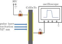
For laser beam-induced transient current measurement, excess carriers are produced by the pulse laser with a wavelength of 527 nm, pulse width of 893 ps, and an energy of 1 μ J/pulse, which has a typical penetration depth of around 530 nm in the CZT detector, much less than the sample thickness. To avoid the space charge effect, neutral density filters each with an optical density of 2, (OD2 means 1% light will be transmitted) are used to control the luminosity of the laser, which induces about 9.8× 1012 mm− 2 photons on the CZT surface. The bias is applied earlier than the pulse laser to obtain a steady electric field. Therefore, plenty of electron– hole pairs can be generated near the cathode, which drift through the crystal under the action of bias voltage and induce a transient current pulse in the external circuit. The induced current signals are recorded by using a digital oscilloscope (Lecoy WaveRunner 610Zi, 1 GHz, 20 GS/s) connected through a 50-Ω resistor. A schematic diagram of the setup used for LBIC measurements is illustrated in Fig. 1.
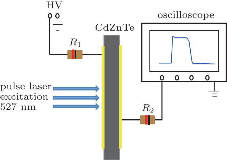 | Fig. 1. A schematic diagram of the setup for the transient current measurements. |
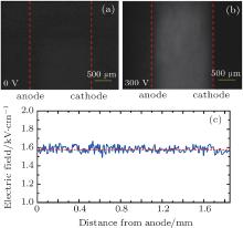
The Pockels electro-optic effect[13] setup is used to measure the distribution of the internal electric field first. Typical Pockels images at 0 V and 300 V are shown in Figs. 2(a) and 2(b). The value of the average internal electric field is calculated by converting the brightness intensity of Pockels images[13, 14] as shown in Fig. 2(c). It shows that the internal electric field is homogeneous and nearly constant.
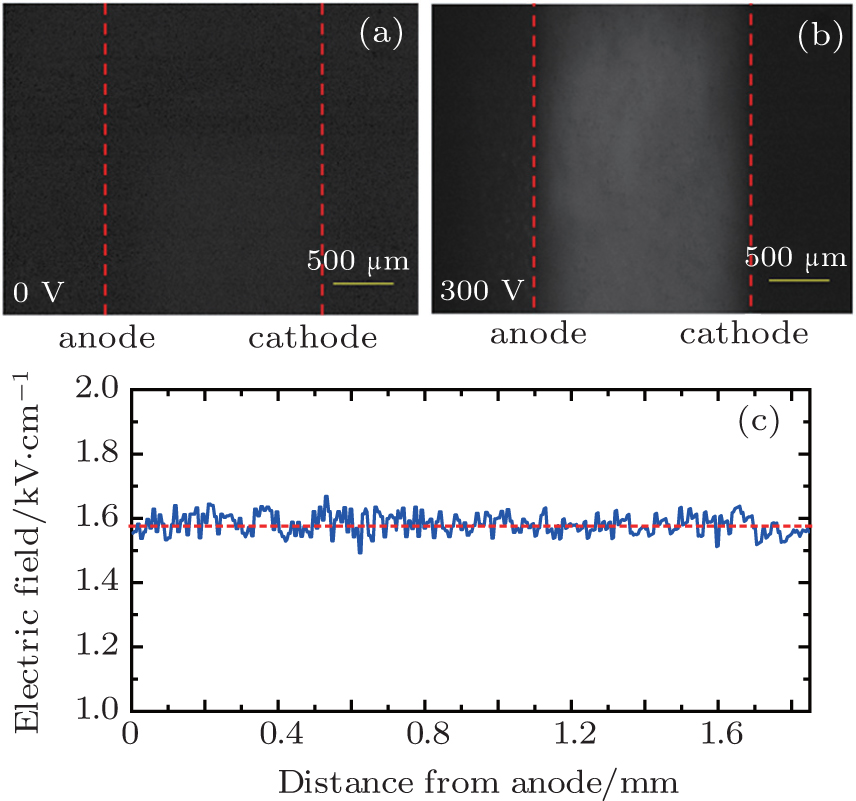 | Fig. 2. Typical Pockels images (polarizers crossed) of (a) unbiased sample and (b) sample biased at 300 V at room temperature; (c) average internal electric field profile along sample thickness. |
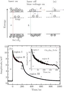
The typical laser-induced transient current waveform of CZT crystal under an electric field of 1081 V/cm and its corresponding physical principle are shown in Fig. 3. The decay part of the current waveform can be roughly divided into three regions. The region I is named the pre-transit region, where the signal decreases rapidly due to the fast surface recombination and the slope of the curve depends on the recombination rate.[12, 15] By fitting the curve in region I, we obtain a surface recombination velocity of 6.14× 105 cm/s. The value of the surface recombination velocity is similar to that found by Cola and co-workers.[16] In region II, the excess carriers keep moving towards the electrodes under the action of the electric field, dominated by the drift process. In the post transit region (named region III), a long tail after tR is present, which should be ascribed to the slow carriers de-trapped from the traps.
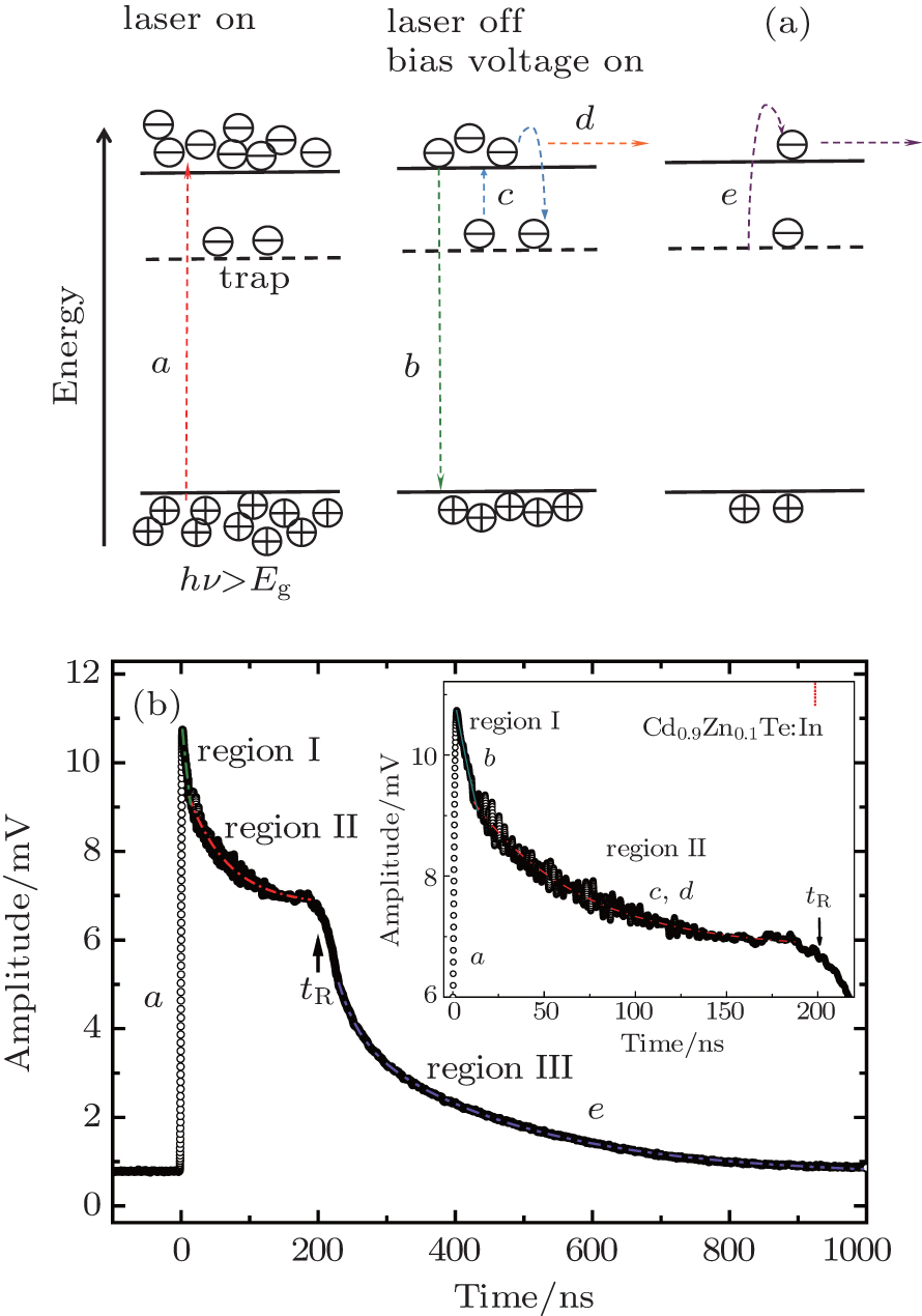 | Fig. 3. Physical processes (a) and corresponding signal parts (b) in laser-induced transient current waveform at room temperature under the electric field of 1081 V/cm with OD2 (OD2 means 1% light will be transmitted), showing a generation and trapping of carriers, b fast recombination process, c trapping and de-trapping process, d drift process, and e reemission of trapped carriers. |
The carriers trapped by crystal defects may be reemitted and contribute to the motion again, present in region II. Such a phenomenon can be described by two parameters, [17] i.e., trapping time τ * and de-trapping time τ D. The solution of the transient current is obtained directly from the basic one-dimensional (1D) transportation equation, [10] on the assumption that the internal electric field is constant and homogenous and the diffusion effect is neglected.[12] The equation can be solved by using Laplace transform under appropriate initial and boundary conditions. For the case where the de-trapping time is less than the transit time, the carriers are reactivated from the traps and contribute to the motion. The transient current is given by[10, 12, 17, 18]
where Q is the total charge generated by the laser pulse, tR is the carrier transit time, τ * is the trapping time, and τ D is the de-trapping time.
By fitting the data in region II with Eq. (1), we obtain a trapping time (τ * ) of 298.3 ns and de-trapping time (τ D) of 65.6 ns directly from the transient current waveform.
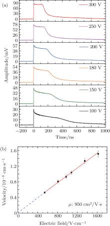
Laser-induced transient current waveforms with different bias voltages are shown in Fig. 4(a). Using a one-level trap model, the parameters of trapping and de-trapping time under bias voltage between 100 V and 250 V are obtained by fitting the waveform (region II) with Eq. (1). The results are shown in Table 1. With increasing the electric field, the transient current waveforms demonstrate clearly an increase in signal amplifier and decrease in duration. The surface recombination velocity also decreases from 1.26 × 106 cm/s to 6.05 × 105 cm/s due to the decrease of electron transit time through the surface region. The trapping time and de-trapping time under the action of a bias voltage of 100 V are calculated to be 372.2 ns and 358.7 ns respectively. Meanwhile, the current waveform follows an exponential-like fall governed by the carrier recombination and trapping process under the action of a bias voltage of 100 V. It is demonstrated that a fraction of the carriers are trapped and cause a fraction of carrier loss, since the transit time (tR) is comparable to the trapping time and de-trapping time under the action of a low electric field, thus the trapping probability increases.
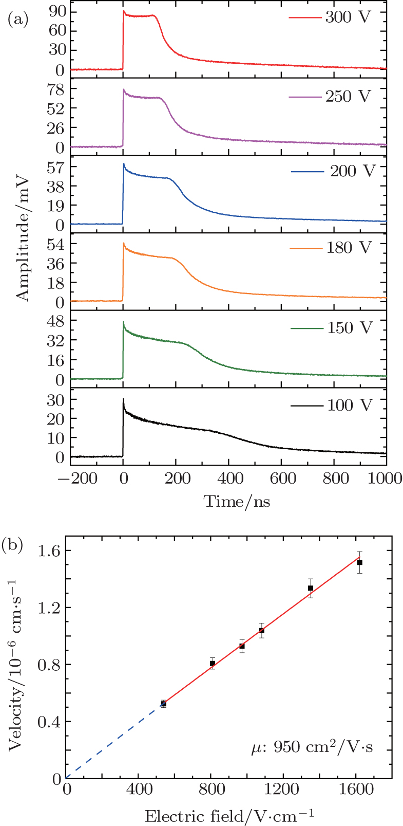 | Fig. 4. The LBIC measurements exposing from cathode side with OD2 (a) laser-induced transient current waveforms measured at different bias voltages, (b) the dependence of the electron drift velocity on electric field strength. |
| Table 1. Cathode irradiation results obtained by fitting the current waveforms. |
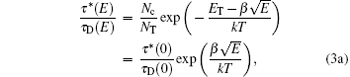
With increasing the electric field, the trapping time and de-trapping time are both decreased; it leads to a field-enhanced carrier capture[19– 21] and emission phenomenon.[22, 23] The capture rate[24]c is defined as

where NT is the concentration of traps, σ is the capture cross section, and υ th is the thermal velocity. The capture cross section increases with the electric field due to the Coulomb attractive effect.[20, 25] On the other hand, according to the Poole– Frenkel effect, [22] with increasing the bias voltage, the trapped carriers reemitted to the conduction band become fast, thus contributing to the motion. The Poole– Frenkel effect also yields an exponential increase of the emission probability τ * /τ D with the square root of the electric field[12, 22, 23, 26] as given by the following equations:
 | (3a) |
 | (3b) |
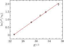
where Nc is the effective density of states in the conduction band, NT is the trap density, ET is the trap ionization energy, k is the Boltzmann constant, and T is the Kelvin temperature, E is the electric field, β = q(q/π ε rε 0)1/2 is the Poole– Frenkel constant, [23] which is calculated to be 3.78 × 10− 4 eV· V− 1/2· cm1/2 in CZT crystal (ε 0, ε r = 10.3 and q is the vacuum- and relative-permittivity, and the electronic charge), τ * is the trapping time, and τ D is the de-trapping time. The dependence of the electron emission probability τ * /τ D on electric field is presented in Fig. 5. The straight line of ln(τ * /τ D) versus 
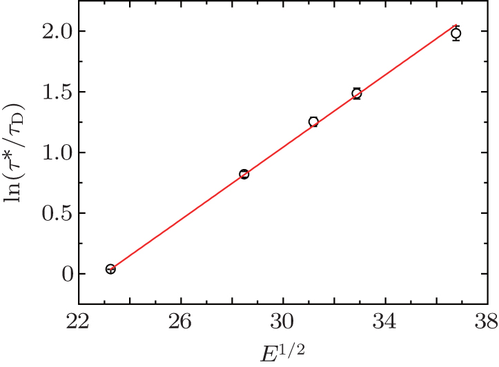 | Fig. 5. Logarithm of the ratio of electron emission τ * /τ D as a function of the square root of the electric field |
For the accurate measurement of the carrier drift velocity, the transit time tR should be clearly determined. After the transit time is measured and the assumption of a constant average electric field is made, the drift mobility is obtained to be, [27]

Figure 4(b) shows the dependence of electric field strength on the electron drift velocity, which shows a linear relationship. The slope of the electric field versus velocity is the mobility of the electrons, which is determined to be 950 cm2/V· s.
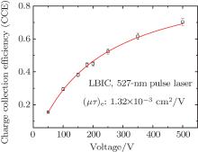
In the LBIC measurement, the collected charge Q is obtained by numerical calculation over a responded current pulse i(t).[12] The dependence of the collected charge on the voltage measured by the LBIC technique is shown in Fig. 6. A modified Hecht relation[15, 16] (Eq. (5)), which accounts for a surface recombination velocity, is used to analyze the charge collection efficiency

where Q0 is the maximum collected charge, s is the surface recombination velocity, and L is the thickness of the sample. The relation between charge collection efficiency and bias voltage is in accordance with a modified Hecht equation. The (μ τ )e value is fitted to be 1.32 × 10− 3 cm2/V with a surface recombination of 1.04 × 106 cm/s. According to the electron mobility (950 cm2/V· s), the lifetime τ is calculated to be 1.38 μ s. However, the lifetime τ obtained from the Hecht equation is a plausible value, which cannot reflect the carrier transport process. Actually, the trapping time and de-trapping time depend on the bias voltage, and misconstruing the lifetime and the trapping time may cause complete obfuscation. To be able to fully exploit the role of defect levels in detector performance, the trapping time as well as the de-trapping time obtained directly from LBIC measurement should be considered, which provides more of a real-world representation of the carrier transport process.
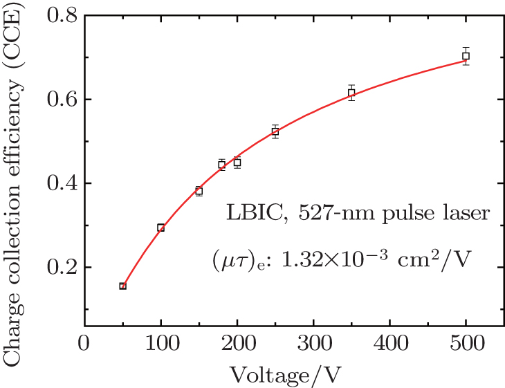 | Fig. 6. Charge collection efficiency as a function of the voltage in LBIC measurement. |
An evaluation method of the carrier transport process and the corresponding physical principle in CZT crystal are presented, which allows an extraction of mobility, trapping, de-trapping time, and electron mobility-lifetime product directly from the LBIC measurement. The electron mobility is calculated to be 950 cm2/V· s. The electron mobility-lifetime product is found to be 1.32× 10− 3 cm2/V on the basis of a modified Hecht equation with considering the surface recombination effect. The trapping time and de-trapping time are found to increase with the decrease of the electric field, which are associated with the field assisted capture and Poole– Frenkel effect respectively. It predicts that the electric field will encourage the carrier emission from trap center due to the lowering of the barrier associated with their Coulomb potential thus causing a higher charge collection efficiency. The measurements demonstrate that the lifetime τ obtained from the Hecht equation cannot reflect the real carrier transport process. The trapping time and de-trapping time obtained from the LBIC measurement provide more of a real-world representation of the charge transport process.
| 1 |
|
| 2 |
|
| 3 |
|
| 4 |
|
| 5 |
|
| 6 |
|
| 7 |
|
| 8 |
|
| 9 |
|
| 10 |
|
| 11 |
|
| 12 |
|
| 13 |
|
| 14 |
|
| 15 |
|
| 16 |
|
| 17 |
|
| 18 |
|
| 19 |
|
| 20 |
|
| 21 |
|
| 22 |
|
| 23 |
|
| 24 |
|
| 25 |
|
| 26 |
|
| 27 |
|