


Linear and nonlinear optical properties of Sb-doped GeSe2 thin films*
[Zhang Zhen-Yinga) , Chen Fena)†  , Lu Shun-Bin
b) , Wang Yong-Huia) , Shen Xiangc) , Dai Shi-Xunc) , Nie Qiu-Huac) ]
, Lu Shun-Bin|
|

 , Lu Shun-Bin
†Corresponding author. E-mail: chenfen@nbu.edu.cn
*Project supported by the National Key Basic Research Program of China (Grant No. 2012CB722703), the National Natural Science Foundation of China (Grant No. 61377061), the Young Leaders of Academic Climbing Project of the Education Department of Zhejiang Province, China (Grant No. pd2013092), the Program for Innovative Research Team of Ningbo City, China (Grant No. 2009B217), and the K. C. Wong Magna Fund in Ningbo University, China.
Sb-doped GeSe2 chalcogenide thin films are prepared by the magnetron co-sputtering method. The linear optical properties of as-deposited films are derived by analyzing transmission spectra. The refractive index rises and the optical band gap decreases from 2.08 eV to 1.41 eV with increasing the Sb content. X-ray photoelectron spectra further confirm the formation of a covalent Sb–Se bond. The third-order nonlinear optical properties of thin films are investigated under femtosecond laser excitation at 800 nm. The results show that the third-order nonlinear optical properties are enhanced with increasing the concentration of Sb. The nonlinear refraction indices of these thin films are measured to be on the order of 10−18 m2/W with a positive sign and the nonlinear absorption coefficients are obtained to be on the order of 10−10 m/W. These excellent properties indicate that Sb-doped Ge–Se films have a good prospect in the applications of nonlinear optical devices.
Ultrafast all-optical switching devices play an important role in modern optical communication systems, in which signals are transmitted at high speed and a high-bit-rate.[1] The silicon waveguide exhibits a larger nonlinearity, [2, 3] however, it manifests strong nonlinear absorption effects, which can restrict the speed of the nonlinear response.[4– 7] Therefore, the new material with high nonlinearity should be explored. In recent years, amorphous chalcogenide glass materials have drawn much attention due to their special physical, electrical, thermal, and optoelectronic properties.[8] Chalcogenide glass containing chalcogens (S, Se, and Te) often has a large nonlinearity and a fast response to the nonlinearity compared with the nonlinear glasses.[9] They have potential applications in optical switches, optical regenerators, wavelength conversion, amplification, etc.[10– 13] Even though more and more groups are involved in the study of optical properties of chalcogenide glasses and thin films, their nonlinear optical parameters are still seldom investigated. Thus, a deep understanding of the linear and nonlinear optical properties of chalcogenide glass is quite important for modern optical communication.
Generally, it is an effective way to change the compositions of the chalcogenide glasses or films for improving the optical properties.[14] The structure of pure Se chalcogenide film is a long polymeric Sen chain, exhibiting instability when heated. Ge– Se chalcogenide films can enhance the network by cross-linking the Sen chain structure to overcome its instability, which makes them useful for the devices in the mid-infrared region. Although Sb-doped GeSe2 (Ge– Se– Sb) thin films have been intensively studied, [15] their nonlinear optical properties, especially the third-order nonlinear properties have not been investigated in depth yet. Our motivation is to extend our knowledge of linear and nonlinear optical properties of Ge– Se– Sb thin films.
In this paper, an effort is made to study the effect of Sb concentration on the linear and nonlinear optical properties of Ge– Se– Sb thin films, which were prepared by a magnetron co-sputtering method. The optical properties of refractive indices and optical band gaps are studied by analyzing transmission spectra. Under femto-second laser illumination in the near-infrared wavelength region (800 nm), the complex nonlinear refractive index and nonlinear absorption coefficient are measured with the laser Z-scan technique.
The Ge– Se– Sb thin films were deposited on clean glass substrates by the magnetron co-sputtering technique. Separated GeSe2 and Sb targets were used in an Ar atmosphere. The substrates were cleaned first by an ultrasonic cleaner, and then distilled water and dipped in acetone followed by ethyl alcohol before loading into the chamber. The chamber was evacuated down to approximately 2.0 × 10− 4 Pa to avoid ambient contamination, and then Ar gas was introduced to 0.25 Pa in each run of the deposition. The sputtering power was tuned in a range from 35 W to 40 W for the GeSe2 target, while for the Sb target the direct current power of 4 W, sputtering pressure of 0.5 Pa, gas flow of 49.8 SCCM (SCCM denotes cubic centimeter per minute at STP) and deposition time of 40 min were maintained.
In order to reveal their structure change with increasing the Sb content the thin films were measured by the x-ray diffraction (XRD) with a diffractometer (BRUKER D2 GMBH) using CuKα radiation (λ = 0.154 nm) at 36 kV and 20 mA. The optical transmission spectra were obtained using a dual beam UV– VIS– NIR Perkin Elmer Lambda 950 spectrophotometer in a wavelength range from 400 nm to 2500 nm. X-ray photoelectron spectroscopy (XPS) was used to confirm the chemical bonding states of the elements. The Z-scan technique was applied to the study of the third-order optical nonlinearities, including the third-order nonlinear refractive index n2 and nonlinear absorption coefficient β . The Z-scan measurements were performed by a mode-locked Ti:sapphire laser, from which a train of optical pulses (central wavelength: 800 nm, pulse duration: 100 fs, 3-dB spectral width: 15 nm, and repetition rate: 1 kHz) were emitted. In order to ensure that the incident laser is adjusted below the optical damage threshold and the multiple-photon effect is suppressed significantly the average power was deliberately controlled below 1 mW by using optical attenuators.
Figure 1(a) shows the XRD patterns of the Ge– Se– Sb thin films. The results of XRD research indicate that the films are maintained in amorphous states and no obvious crystalline phases occur with the addition of the Sb element in our experiment. Optical transmission spectra of Ge– Se– Sb thin films are given in Fig. 1(b). It shows that there is a reasonable transmission region for all the films. Judging from the spectra, as the Sb content increases, a noteworthy red shift can be observed in the interference free region.
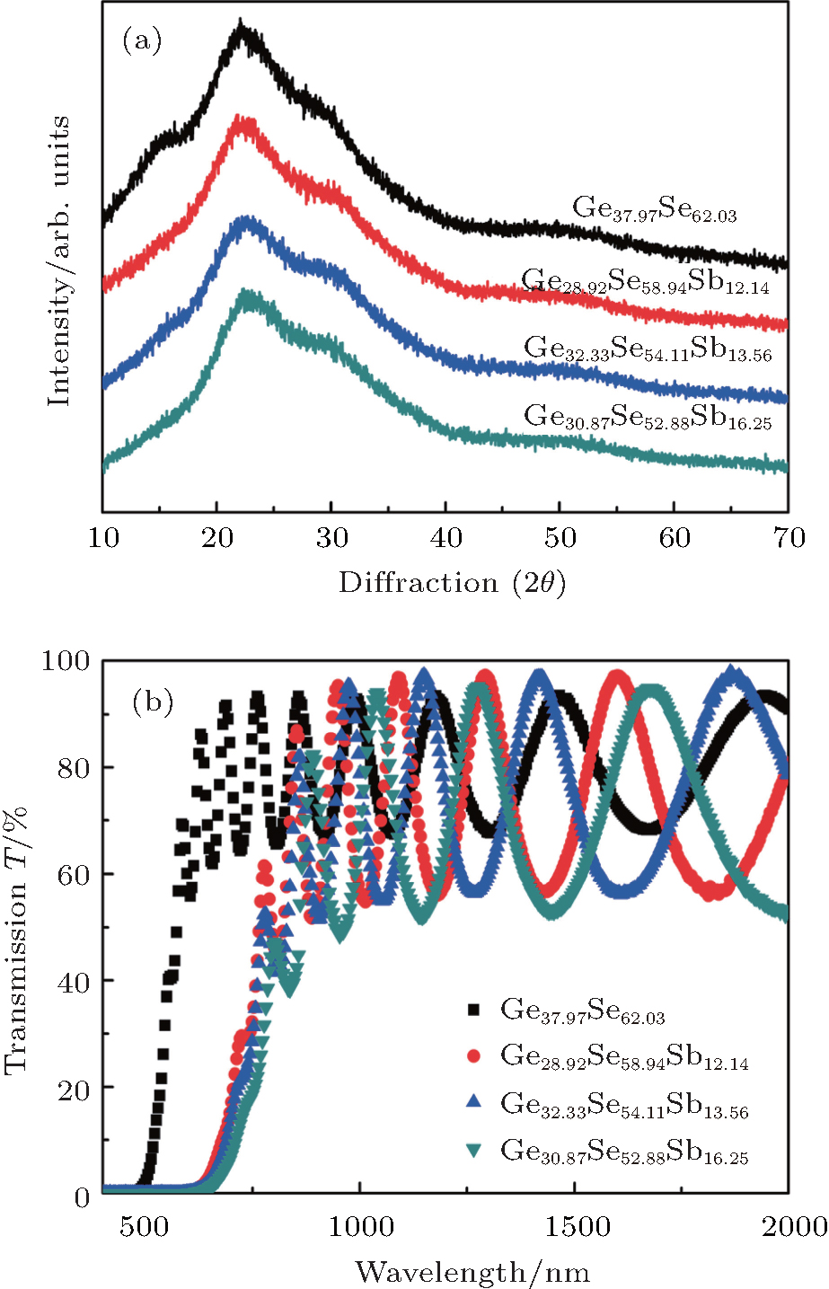 | Fig. 1. (a) XRD patterns and (b) the typical transmittance spectra of Ge– Se– Sb thin films on glass substrate. |
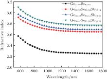
Figure 2 shows the variations of refractive index with wavelength. The refractive index is derived by their transmission spectra using Swanepoel’ s envelope method, [16] which is based on the maximum and minimum transmittance fringes. It is clear that the refractive index is enhanced with increasing the Sb content. According to the Lorentz– Lorenz relation between refractive index and polarizability, the refractive index will become larger with the increase of polarizability.[17] Since the atomic radius of Sb (1.40 Å ) is larger than those of Ge (1.22 Å ) and Se (1.17 Å ), the refractive index of the Ge– Se– Sb thin film increases with increasing the Sb content.
 | Fig. 2. Variations of refractive index with wavelength for the Ge– Se– Sb thin films. |
The dispersion parameters can be analyzed by the Wemple– DiDomenico (WDD) model.[18] The high frequency property of film could be treated as that of a single oscillator. Therefore, the optical parameter could be estimated by the following relation:

where E0 is the single-oscillator energy, and Ed is the dispersion energy. The E0 and Ed can be determined by plotting refractive index factors (n2 − 1)− 1 against (hv) 2 and fitting straight lines in Fig. 3. The values of E0 and Ed for all the compositions are given in Table 1. The E0 is related to the average bond energy of different chemical bonds present in the material. It can be observed that E0 decreases with increasing the content of Sb in Ge– Se– Sb thin film. The reason is due to the lower bond energies of Sb– Se (183.89 kJ/mol) than those of Ge– Se (206.77 kJ/mol) bonds.[19] According to Tanaka, [20]E0 is equal to twice the optical band-gap Eg approximately. This is also well supported by data in Table 1. The static refractive index (n0) of the Ge– Se– Sb thin film is calculated from WDD dispersion parameters E0 and Ed via using the formula
The n0 at 800 nm is calculated by extrapolating the WDD dispersion equation to hv → 0. It can be seen from Table 1 that n0 increases with the increase of Sb content.
 | Fig. 3. Plots of the refractive index (n2− 1)− 1 versus (hv)2 for Ge– Se– Sb thin films. |
| Table 1. Summary of the values of linear refractive index n and static refractive index (n0) at 800 nm, dispersion energy (Ed), single oscillator energy (E0), and optical band gaps (Eg) of Ge– Se– Sb thin films. |
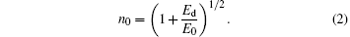
As is well known, the optical energy gap can be determined according to the ‘ non-direct transition’ model for amorphous semiconductors proposed by Tauc equation[21]

where B is a constant, hv is the photon energy, and Eg is the Tauc optical band gap. The optical band gap Eg is obtained by extrapolating the linear portion of the plot to the energy axis. The plot of variation of (α hv)1 / 2 versus hv is shown in Fig. 4. It is clear that the optical band gap decreases from 2.08 eV to 1.41 eV with increasing the Sb content. The variation could be interpreted on the basis of the chemical-bond theory proposed by Bicerano and Ovshinsky.[22] When the Sb content is increased, due to the fact that in the sample there are not enough Se atoms to satisfy the valence requirements of Sb by the nearest neighbors of Se atoms, there are still redundant Sb atoms, which must be satisfied by forming Sb-rich units. These dangling bonds will lead to the formation of localized states in the gap, which causes a decrease in the optical band gap of the Ge– Se– Sb thin film. The following discussion about XPS spectra confirms this analysis.
 | Fig. 4. Plots of (α hv)1 / 2 versus hv for the Ge– Se– Sb thin films. |
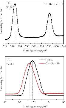
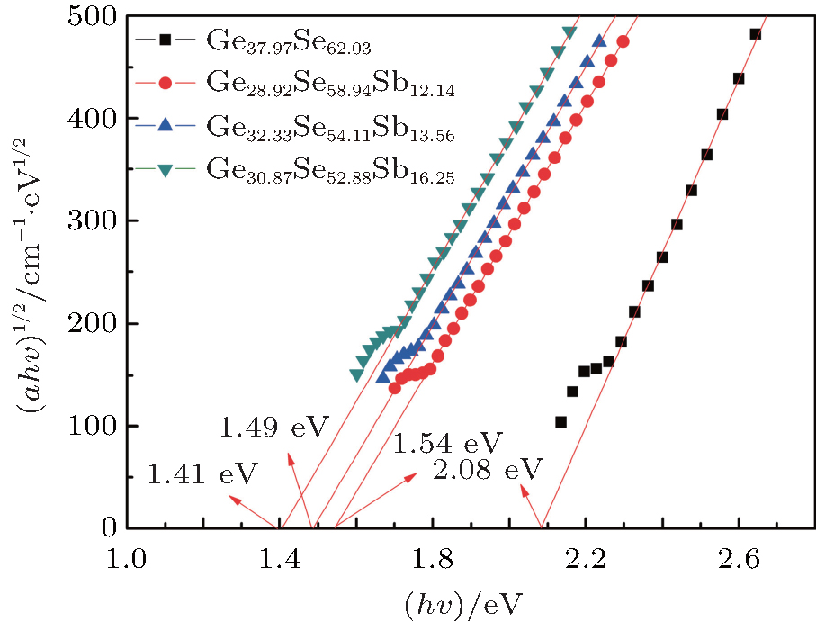
The XPS spectra are further used to understand the binding state in Ge– Se-Sb thin film, and the results are shown in Figs. 5(a) and 5(b). As illustrated in Fig. 5(a), the peaks of Sb 3d are detected approximately at 526.78 eV and 536.28 eV. As is well known the binding energy of the A element, which bonds with the B element, decreases if the B element is replaced by the C element that has lower electronegativity.[23] Since the electronegativity of Sb (2.05) is smaller than that of Se (2.55), the binding energy of Se 3d spectra will decrease if part of the Se atoms in the Ge– Se bond are replaced by Sb atoms. If we compared the Se 3d spectrum of the Ge– Se– Sb film with that of GeSe2 film in Fig. 5(b), the peak position shifts toward a lower binding energy, indicating that Sb– Se bonds form in Ge– Se– Sb thin film. As is well known the optical band gap is related to the bond energy. The bond energy of Sb– Se (183.89 kJ/mol) is much lower than that of Ge– Se (206.77 kJ/mol). Therefore, the formation of Sb– Se bonds reduces the energy of the system, which will reduce the optical band gap with increasing the Sb content.
 | Fig. 5. XPS spectra of (a) Sb 3d and (b) Se 3d for as-deposited Ge– Se– Sb thin film. |
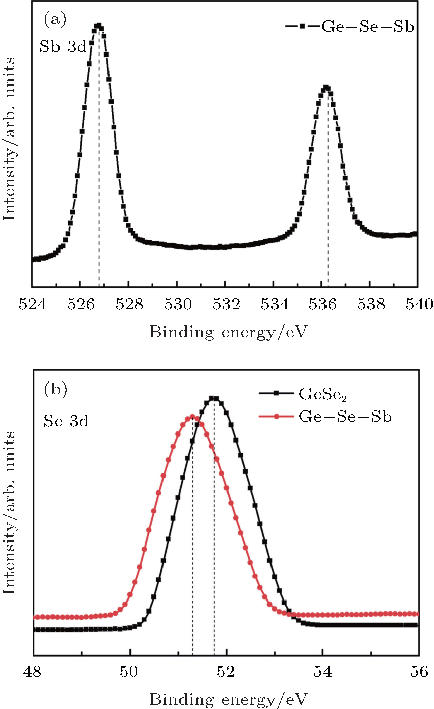
As a strong electric near-field can induce large optical nonlinearities, the third-order nonlinear absorption and refraction properties of the Ge– Se– Sb thin film can be further investigated using Z-scan measurements at 800 nm. The Z-scan is considered to be a very useful technique to probe the nonlinear optical response of material, given that it allows for high sensitivity detection as well as an excellent ability to simultaneously measure the magnitude and sign of the nonlinear refraction and absorption, which has been used widely for the nonlinear optical measurement in our previous work.[24, 25]
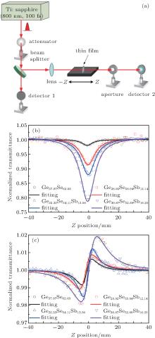
The Z-scan experimental setup is shown in Fig. 6(a). The empty circles in Figs. 6(b) and 6(c) represent the typical results of the open aperture and closed aperture transmittance T each as a function of sample position for different Sb concentrations, respectively. The empty symbols denote the measured data while the solid lines are for the fitted curves. The open-aperture measurement enables one to investigate the nonlinear absorption, while within the closed aperture measurement the change of optical transmittance is a combined consequence of the nonlinear absorption and the nonlinear refraction induced by the optical Kerr nonlinearity. The division of the closed-aperture measurement by the open-aperture measurement will yield the separation of these two effects.[26] When the nonlinear absorption and refraction are presented simultaneously in the sample, the normalize transmittance T dependence in the closed aperture output can be written as follows:


where x = z/z0 with 
 | Fig. 6. (a) Schematic diagram of the Z-scan experimental setup. (b) Open-aperture and (c) the division of the closed-aperture measurements by the open-aperture measurements Z-scan curves of Ge– Se– Sb films at 800 nm. The empty symbols represent the experimental data and the solid lines denote fitting curves. |
| Table 2. Nonlinear optical parameters of Ge– Se– Sb thin films. |
As shown in Fig. 6(b), when the object lens is translated across the focus point (Z = 0), each of all the measured open aperture Z-scan curves shows a valley-like shape, implying that the third-order nonlinear absorption of the Ge– Se– Sb thin film is reverse saturation absorption (RSA) induced by the two-photon effect. The valley appears at the focus point where the laser pulse has the strongest influence. Figure 6(c) displays the typical shapes of all closed aperture Z-scan traces which are asymmetric with respect to the focus point (Z = 0). The observation implies that both the nonlinear absorption and the nonlinear refraction take place simultaneously. The profile with a valley followed by a peak in the closed aperture normalized transmittance output represents the positive nonlinear refractive index, which results from the optical nonlinear refraction and self-focusing nonlinear response in the sample.
By comparing the values of n2 and β in Table 2, we can conclude that the measured nonlinear properties increase with increasing Sb dopant concentration. The measurement values of n2 of the Ge– Se– Sb thin films are all on the order of 10− 18 m2/W, which is about one order larger than that of the undoped Ge– Se-based thin film. According to Miller’ s rule, [27] the larger the linear refractive index, the greater the nonlinear refractive index will be. Generally, the nonlinearities based on the free carrier effects are significant for laser pulses of picosecond pulse duration and longer. In our experiment, a femto-second laser is used for the Z-scan measurement. Therefore, the free-carrier effect is negligible.[27] While the films are being irradiated by a laser, they may be influenced by the local heating, but the laser repetition rate (kHz) is much smaller than MHz in our experiment. Therefore, the nonlinear refractive index of the Ge– Se– Sb thin film is not affected by thermal effects. More work is needed to further study the third-order nonlinear properties of these thin films.
Chalcogenide Ge– Se– Sb thin films are deposited successfully on glass substrates at room temperature by a magnetron co-sputtering method. XRD analyses reveal that the as-deposited films are amorphous. The values of the refractive index and the optical band gap of the thin films are obtained by transmission spectroscopy. It is found that the optical band gap decreases and the refractive index increases with increasing the Sb content. XPS analysis further shows that Sb– Se bonds can reduce the optical band gaps of films. The third-order nonlinear optical properties of the as-deposited films are measured by the Z-scan technique at a wavelength of 800 nm. The results show that the nonlinear optical properties are enhanced with the concentration of Sb increasing. The values of nonlinear refractive index n2 and absorption coefficient β of Ge– Se– Sb thin films are obtained to be on the order of 10− 18 m2/W and 10− 10 m/W, respectively.
In our future work, chalcogenide Ge– Se– Sb composition will further be optimized to improve the refractive indices of films and make them possess high third-order nonlinear properties for the application of nonlinear optical devices.
| 1 |
|
| 2 |
|
| 3 |
|
| 4 |
|
| 5 |
|
| 6 |
|
| 7 |
|
| 8 |
|
| 9 |
|
| 10 |
|
| 11 |
|
| 12 |
|
| 13 |
|
| 14 |
|
| 15 |
|
| 16 |
|
| 17 |
|
| 18 |
|
| 19 |
|
| 20 |
|
| 21 |
|
| 22 |
|
| 23 |
|
| 24 |
|
| 25 |
|
| 26 |
|
| 27 |
|