


Effect of deposition parameters on structural and mechanical properties of niobium nitride synthesized by plasma focus device*
[Siddiqui Jamila), b) , Hussain Tousifa)†  , Ahmad Riaz
a), b) , Khalid Nidab) ]
, Ahmad Riaz|
|


†Corresponding author. E-mail: tousifhussain@gcu.edu.pk
*Project supported by the HEC, Pakistan.
Effects of deposition angle and axial distance on the structural and mechanical properties of niobium nitride synthesized by a dense plasma focus (DPF) system are studied. The x-ray diffraction (XRD) confirms that the deposition parameters affect the growth of multi-phase niobium nitride. Scanning electron microscopy (SEM) shows the granular surface morphology with strong thermally assisted coagulation effects observed at the 5-cm axial distance. The non-porous granular morphology observed at the 9-cm distance along the anode axis is different from those observed at deposition angles of 10° and 20°. Energy dispersive x-ray (EDX) spectroscopy reveals the maximum nitrogen content at the shortest (5 cm) axial position. Atomic force microscopy (AFM) exhibits that the roughness of coated films varies for coatings synthesized at different axial and angular positions, and the Vickers micro-hardness test shows that a maximum hardness value is (08.44 ± 0.01) GPa for niobium nitride synthesized at 5-cm axial distance, which is about 500% more than that of a virgin sample.
The transition metals with interstitially implanted small atoms of nitrogen and oxygen form an exclusive class of compounds, which exhibits unique and diverse physical as well as chemical properties.[1, 2] High hardness, good corrosion and abrasion resistance, high melting points, low electrical resistivity, biocompatibility, and oxidation resistance have aroused the interest of researchers in these nitrides and oxy nitrides.[3– 7] Among this family, niobium nitride is a prominent entrant due to its various attractive properties, such as mechanical strength along with wear resistance, chemical inertness, good stability at high temperatures, lower electrical resistivity, and high melting point.[8, 9] These salient properties have made niobium nitride film an appropriate material choice for protective coatings, wear resistant coatings, single-photon detectors, Josephson junctions, field emission cathodes, and diffusion barriers against copper migration in microelectronics.[3, 10– 13]
The addition of oxygen content into the metallic nitride films induces progressive changes in film characteristics. Even incorporation of an adequate quantity of oxygen into niobium nitride can stabilize its phase in moderate quantity.[14] Though conversion of niobium nitride into niobium oxy-nitrides (NbOxNy) has often been observed, it is worth highlighting that niobium oxy-nitrides possess better properties in some applications than niobium nitrides.[6] Fenker et al. have fabricated niobium oxy nitride and niobium oxide coatings by reactive-pulsed magnetron sputtering in an oxygen and nitrogen environment and found that the hardness values of the films range from 6 GPa to 8 GPa.[15]
Various techniques have previously been employed for niobium nitride film coatings, which mainly include reactive magnetron sputtering, [16] ion beam assisted deposition, [17] pulsed laser deposition, [18] and filtered arc deposition.[19, 20] Though niobium oxy-nitride films have been synthesized mainly by physical vapor deposition (PVD) techniques, [4, 5, 21] the CVD has also been employed for their growth.[22] In addition to these techniques, unintentional formation of niobium oxy nitride phases at the NbN interface has also been observed.[6]
The dense plasma focus (DPF) device is a hydromagnetic coaxial plasma accelerator where the high-current electrical discharge efficiently heats and compresses the plasma into a pinched plasma column where a short lived hot (1 keV– 2 keV) and dense (1025 m− 3– 1026 m− 3) plasma is produced. The energy density (the ratio of the electrical energy stored in the capacitor bank to the volume of the final cylindrical pinched plasma column) of the DPF device is reported to be in a range of 1.2 × 10¹⁰ J/m3– 9.5 × 10¹⁰ J/m3, which makes it a high energy plasma facility.[23] The dense and hot plasma produced by the device has also been acknowledged as a multiradiation source of highly energetic ions, [24] relativistic electrons, [25, 26] neutrons, [27] and intense bursts of x-rays.[28] Due to the broad energy spectrum of radiation emanated in the plasma focus, its application in material processing has shown prominent features of better adhesion and good deposition rates.[29, 30] Numerous properties and features of DPF, which have made it an exclusive and attractive source for thin film depositions and material processing, have been reported by Rawat in a recent review paper.[31]
Most recent applications of DPF are in the field of bulk material processing along with thin films growth by making use of pulses of energetic ions emanated from dense and hot decaying plasma. Many researches have employed ion beams emitted from DPF for room temperature plasma processing of materials including ion implantation, surface modification, thermal surface treatment, phase changes of thin films, and thin film deposition.[32– 36]
In this research, plasma-emanated energetic ion beam pulses in DPF are employed for niobium nitride/niobium oxy-nitride coatings at room temperature. The small size, significantly low cost, easy maintenance, and technically simple construction and operation of this hybrid facility are the main reasons for its selection in the present research. Multi-technique characterizations including XRD, SEM, EDX, AFM, and the Vickers hardness test are employed to relate coating properties to synthesis conditions.
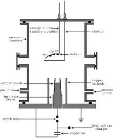
A Mather-type DPF device is employed for the synthesis of film coatings in the present experiment. The device is powered by a 30-μ F, 15-kV Maxwell capacitor. A schematic diagram of the plasma focus system is presented in Fig. 1.
 | Fig. 1. Schematic diagram of dense plasma focus device. |
The technical parameters of the device are given as follows. Operational charging voltage is kept at 12 kV throughout the experiment for all coatings, which leads to an energy of 2.3 kJ and a maximum discharge current of 175 kA. The aggregate inductance of the system was about 80 nH. The main chamber is made of stainless steel, which is evacuated up to 10− 2 mbar (1 bar = 105 Pa) by a rotary vane pump. Afterward, high purity nitrogen gas is filled into the chamber. The filling gas pressure is kept constant at an optimum value of 1.25 mbar. The device employs a copper-made solid cylindrical anode surrounded by six cylindrical copper rods constituting the cathode. The anode was concaved from the tip in order to minimize the impurities in the plasma.[37] A slightly tapered anode from the open end is used as it has been reported that tapering enhances the emission of ions, electrons, and x-rays from the pinched plasma.[38] A pyrex made sleeve is used for the separation of electrodes. The main assembly chamber of the device and the cathode rods are both connected to the ground potential. The other details of the DPF device are provided elsewhere.[39] A qualitative description of the plasma formation and film coating process in the DPF device is as follows.
When electrical energy stored in the capacitor bank is delivered to electrode assembly through the spark gap switch, the breakdown of gas present in the chamber takes place in the vicinity of the insulator sleeve. This breakdown results in the formation of an axis symmetric current sheath, which is influenced and accelerated by the Lorentz force. The current sheath spreads uniformly outwards towards the cathode rods in an inverse pinch phase and then accelerates upwards towards the open end of the electrodes in an axial rundown phase. The sheath collapses radially inwards on reaching the open end of electrode assembly, resulting in the creation of short lived (∼ 10 ns– 50 ns), dense (∼ 1026 cm− 3) and hot (∼ 1 keV) pinched plasma just above the anode tip in the final focus phase. It is worth noting that in the plasma focus device the plasma temperature and density are approximately two to three and about three to ten orders of magnitude respectively higher than cold (low temperature) plasma. Formation of a pinched plasma column is subsequently followed by sausage (m = 0) instability, which enhances the induced electric field locally, that couples with the magnetic field, resulting in the disruption of the plasma column.[40] The disruption of the plasma column leads to the acceleration of highly energetic ions towards the top of the chamber, and relativistic energies electrons (∼ 100 keV above) in the downward direction towards the positively charged anode.
Thus the samples exposed to DPF are treated by a mixture of energetic ions flux, decaying hot and dense plasma, strong shock wave, and speedy ionization wavefront during each plasma focus shot.[31] The main processes occurring in DPF during the sample processing are described as follows.[41]
(i) Accelerated ions strike the sample resulting in high thermal gradients due to sufficient energy transfer. Consequently, abrupt heating followed by rapid cooling effects are generated in the sample surface. These ions, besides etching and cleaning the sample surface, implant into the sample surface forming metallic nitride.
(ii) Energetic ions reaching the sample increase the surface temperature, resulting in local melting and evaporation of the sample, that may chemically react with the succeeding ions to form metallic nitride, which is deposited again on the sample surface. Thus compound layer coating is likely to be initiated on the sample surface.
(iii) The downward accelerated electrons accompanied with the hot dense pinched plasma are energetic enough to ablate the anode top material, which may result in the deposition of undesirable debris on the exposed sample surface.[31] Yet the problem is minimized to a very large extent by using a deep hollow anode with a relatively thin wall. Thus, in our case, exposed (niobium) samples are processed mainly by instability-accelerated energetic ions and decaying hot and dense plasma streams generated from the tight elongated pinched plasma column.
The features of the plasma focus device such as high heating rate (∼ 15 K· ns− 1) and temperature gradient (1500 K· mm− 1) makes the device feasible as an ion implanter, which can perform nitriding in a short interval of time.[42] The ions and electrons are emanated out of the decaying pinched plasma column in more than one bunches of a time period that is about a few tens of nano-seconds. Ions emission exhibits fountain resembling geometry with anisotropic behavior in an angular distribution. Most of the energetic ions emerged in a small solid angle with respect to the anode axis and their flux decreases with the increase in angular position. The majority of highly energetic ions emerged out in an angular range from about 0° to 10° – 20° with respect to the anode axis.[31]
Niobium (99.95% purity) samples with 10 mm × 10 mm × 0.50 mm in dimension are used for film coatings. Before being placed in the chamber, the samples are cleaned in an ultrasonic bath, using acetone and alcohol respectively for about 15 min. After being cleaned, they are placed on the sample holder along the anode axis at the different axial distances of 5 cm, 9 cm, and 13 cm from the anode tip. The coatings are also synthesized at different angular position 0° , 10° , and 20° for 9-cm axial distance position. Samples are placed on a specially designed holder for synthesis of film coatings at different angular positions with respect to the anode axis. A bent substrate holder is used to keep axial distances of samples approximately the same from the top of the anode. The number of plasma focus shots is kept constant at 30 for coatings at all axial and angular positions. To avoid unnecessary exposure of samples during focus shots taken to attain a good focusing condition, an externally controlled movable shutter is placed between the anode and the substrates, and removed after availing good focusing. Rogowski coil and high voltage (HV) probes are employed to observe and record the current and voltage waveforms. A Tektronix TDS 3054B (four channel real-time digital) oscilloscope (500 MHz, 5 GS/s) is used during the experiment to record the signals from Rogowski coils and the high voltage (HV) probe. The voltage and current curves are used for optimizing the device. The strong focusing action is indicated by the presence of an intense voltage spike in the high voltage signal and by a steep current dip in the Rogowski coil signal. An efficient energy transfer accompanied by heating the plasma column is ensured by a strong focusing.[42, 43]
The x-ray diffraction (XRD) technique using a Philips X’ Pert PRO MPD theta-theta x-ray diffractometer operated at a voltage of 40 kV and current of 40 mA with Cu Kα (λ = 1.54 Å ) radiation is used to characterize the niobium nitride deposited film and reveal the structural analysis of the film. The machine is used in detector scan mode to perform a 2θ scan over the 20° – 80° range. Scanning electron microscopy (SEM) using the JEOL JSM-6480 LV with the energy dispersive x-ray (EDX) attachment is used to investigate the surface morphologies and the elemental compositions of the deposited films. The roughness of the film is characterized by atomic force microscopy (AFM). A Wilson Wolpert 401MVA Vickers Micro-hardness tester is used to measure the surface hardness values of coated films with different test loads.
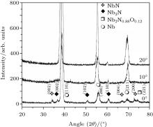
The x-ray diffractograms of samples exposed at different axial positions from anode tip along the anode axis are shown in Fig. 2. The XRD pattern of virgin niobium is also presented for comparing and studying the extent of crystallographic modification induced in films during the samples exposure at different axial distances.
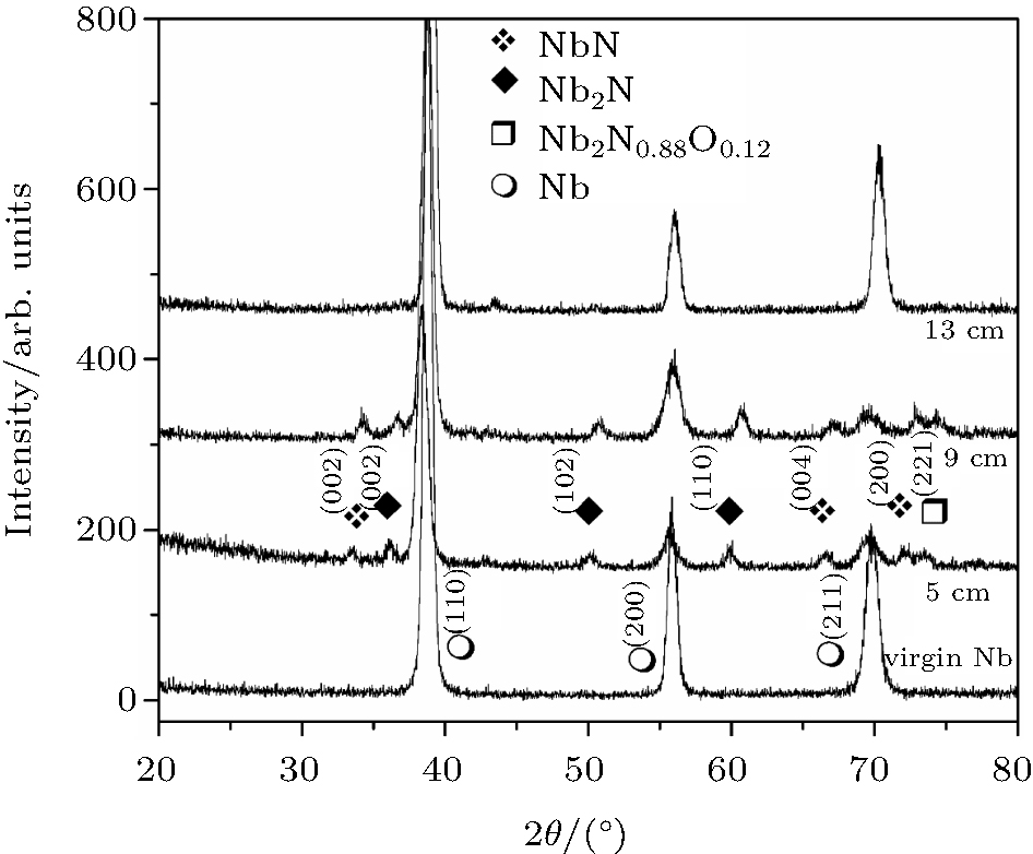 | Fig. 2. The x-ray diffractograms of samples exposed to 30 plasma focus shots at different axial positions (5 cm, 9 cm, and 13 cm) from anode tip along the anode axis. |
Un-treated niobium has three diffraction peaks. A diffractogram of the sample placed at 5 cm shows the emergence of new peaks of niobium nitride, which are identified as hexagonal phases of NbN (002), (004), (200) and Nb2N (002), (102), and (110) phases along with peaks of niobium with significantly reduced intensities.[44, 45] The reduced peak intensities corresponding to niobium planes suggest the degradation of crystallinity in niobium phase, which is attributed to higher ion energy and flux at this axial position. Higher abundance of low energy ions (< 100 keV) as compared with other ion energies, is found irrespective of angular position with respect to anode axis.[46] It is found that ion number density and the corresponding probable nitrogen ion energy decrease from 10.1 × 1013 cm− 3 to 4.3 × 1013 cm− 3 and from 82 keV to 57 keV respectively when the axial distance is increased from 3 cm to 9 cm in the DPF device.[47] In addition to reduced intensity, a little downshifting in all diffraction peaks from the corresponding standard stress-free positions is also observed, which is attributed to residual stresses induced in the film caused by ion implantation through successive focus shots. Plasma assisted ion implantation creates lattice distortions (strains), resulting in variation of d-spacing, which leads to the shifting of diffraction peaks from the corresponding standard stress free data. Strong thermal shocks produced in each focus shot are also responsible for the induced tensile stresses indicated by a downshift at the peak position from standard stress free positions.[48]
A similar sort of downshifting in peaks at 5-cm axial distance is also observed for modifying the surface of Al alloy by nitrogen ion implantation in the plasma focus device.[49] The instability accelerated ions emanated from plasma have a wide energy range and are of a fountain-like geometry with anisotropic angular distribution. These highly energetic ions strike the niobium substrate and transfer sufficient energy at a fast rate to the substrate, which immediately attains high temperature, resulting in local melting and evaporation.[50] The nitrogen ion beam produces a strong heating effect on the superficial layer of the sample surface (up to the melting point), thus favoring the diffusion of the impinging particles during its liquid phase.[49]
The growth process of NbN/Nb2N film in the plasma focus device is mainly comprised of two processes: i) implantation of energetic nitrogen ions in niobium creating point defects and lattice distortion by their interstitial incorporation and ii) re-deposition of evaporated niobium (and oxygen) from the surface after reaction with nitrogen ions due to backscattering of ablated material by filling gas at a relatively higher pressure.[51] The emergence of a new phase of niobium nitride may also be due to the adsorption of energetic species (particularly nitrogen ions) in the substrate surface.[52]
The shifting of peaks caused by the increase in d-spacing is observed to decrease gradually for samples placed at axial positions 9 cm and then 13 cm as compared with that at axial position 5 cm; which may be due to the decrease in the ion energy at an increased distance from the anode tip, causing less penetration of ions. Hassan et al.[47] has reported that (nitrogen) ion energy and their number density decrease with increasing the axial distance in the plasma focus device.
A slight increase in the crystallinity of all phases of niobium nitride (NbN/Nb2N) is also observed for coating synthesized at 9-cm distance, suggesting that the ion energy and flux at this axial distance are appropriate for better crystallinty of niobium nitride phases.
Along with the formation of multi-phases of niobium nitride, a small weakly crystalline peak of niobium oxy nitride Nb2N0.88O0.12 is also observed for 5-cm and 9-cm positions, which may be attributed to the residual gas pressure. The native oxide present on the sample may also cause the formation of this oxy nitride phase of niobium. In the plasma focus device, multi-phase coatings with the minimization of the free energy of the surface are induced by ion adsorption. The substrate system readily having high surface energy from the energetic ions bombardment will not always be converted into low energy state due to kinetic barriers involved in the restructuring process. The growth of meta-stable (non-stoichiometric) phases is favorably attributed to higher surface free energy.[53] This is revealed in the appearance of non- stoichiometric phases of niobium oxy-nitride at 5-cm and 9-cm axial distances, associated with higher energy flux.
No obvious peak other than that of the niobium phase is observed for the 13-cm axial position. It can also be noted that the peak positions and intensities of niobium phases are also almost the same as those in un-treated niobium. The disappearance of NbN/Nb2N/Nb2N0.88O0.12 phase can be attributed to the fact that this axial position cannot be covered by nitrogen plasma or the energy of nitrogen ion is not enough for film coating.
The x-ray diffractograms of samples exposed to 30 plasma focus shots at different angular positions (0° , 10° , and 20° ) for 9-cm axial distance are represented in Fig. 3.
 | Fig. 3. The x-ray diffractograms of samples exposed to 30 plasma focus shots at different angular positions (0° , 10° , and 20° ) from anode tip at 9-cm axial distance. |
Two main features are clearly observed in the spectra. Firstly, the crystallinities of niobium nitride and niobium oxy-nitride decrease with increasing the angle of sample exposure. Secondly; the diffraction peaks of niobium start to regain the intensity of a virgin sample with increasing the angle. A highly anisotropic behavior exists in the angular distribution of ions with respect to the anode axis. This high anisotropy in ion emission may be attributed to the emission of ions from various micro-sources created in the pinched plasma column as reported. The maximum ion density (2.20 × 10¹⁹ m− 3) is found to be in the case with the deposition angle in a range from 0° to 5° (with respect to anode axis), and to decrease down to 4 × 10¹⁸ m− 3 – 8 × 10¹⁸ m− 3 at 10° angular position.[46] It has been reported that ions originate from different (non-symmetrically distributed with respect to the anode axis) micro-ion sources generated in the plasma column. The majority of ions are observed to emanate between 0° and 11° because the magnetic field of plasma favors the emission of ions in the vicinity of the anode axis, [54] therefore, the ion flux in the plasma focus device decreases with the increase of angular position and hence the irradiations at higher angles of 10° and 20° will result in a low level of nitrogen ion implantation as well as lower ablation assisted deposition of composite (NbN/Nb2N/Nb2N0.88O0.12) film coating.
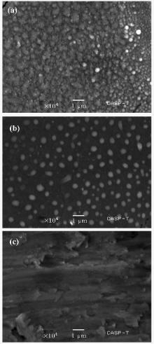
Scanning electron microscopy (SEM) using JEOL JSM-6480 LV equipped with an energy dispersive x-ray (EDX) attachment is used to investigate the surface morphology and the elemental composition of film coating. Micrographs in Fig. 4 show the surface profiles of virgin niobium and synthesized coatings at different axial positions for 30 focus shots at 0° angular position.
Figure 4(b) shows the surface morphology of the sample exposed at 5-cm axial distance. A granular surface morphology with a strong thermally assisted coagulation effect due to the higher ion energy flux at this axial position is observed. Because of the large energy transferred to the substrate, the defects are developed and subsequently the nucleated structures on a nanometer scale are created. Nucleates with a size of up to a few tens of a nm are grown through ion-induced collision cascade for ion energies ranging from several tens of keV to MeV.[55] The successive focus shots increase the substrate temperature significantly, favoring nanoparticulate coagulation as observed for 5-cm position.
A uniform, thick, and non-porous granular morphology without any crack is observed for the 9-cm axial distance at 0° angular position [Fig. 4(c)]. The granular surface is primarily composed of closely packed nanospheroids which are distributed quite homogeneously over the coated film. It has
 | Fig. 4. Scanning electron micrographs of (a) untreated and treated samples at (b) 5-cm, (c) 9-cm, and (d) 13-cm axial distances along the anode axis with fixed 30 plasma focus shots. |
been reported that the ion irradiation process in the plasma focus device is similar to transient thermal annealing and causes re-arrangement of atoms in the surface layer, resulting in the formation of nanoparticles.[41] As the bunching of nanoparticles is energetically favored, therefore it can be assumed that high surface energy and bond interactions among multiple phases of nanocomposite causes the gathering of primary nucleates into spherical agglomerates.[53] It can be seen that no such definite coagulation pattern is observed for the sample placed at 13 cm [Fig. 4(d)] because of attenuation of ion flux at a larger axial distance.
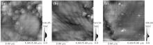
Figure 5 represents a morphological comparison of coatings achieved at different angular positions at the 9-cm axial distance. For 10° angular position [Fig. 5(b)], less rough surface with well dispersed grains than that for the 0° angular position is
 | Fig. 5. SEM micrographs of samples exposed to 30 plasma focus shots at (a) 0° , (b) 10° , and (c) 20° angular position at 9-cm axial distance. |
observed. The white shiny nano bubbles present on the surface probably represent the presence of niobium nitride/niobium oxy-nitride as it is a major contributor in the film. The greater dispersion of grains at the 10° angle is attributed to the decrease in ion energy and flux with increasing the angular position with respect to the anode axis. The coated surface for 20° angular position [Fig. 5(c)] does not show any nanospheroid, owing to the minimum flux of ions as compared with for 0° and 10° angular positions.
The EDS technique is employed for investigating the elemental compositions in film coatings synthesized at various axial and angular positions.
| Table 1. The EDS data presenting elemental concentrations (at.%) for various film coatings achieved at different axial and angular positions. |
The maximum nitrogen content is approximately 24.56 at.% present in the surface of the coated film deposited at the 5-cm axial position, confirming the maximum coating at this axial position due to the maximum ion energy and flux. This is in agreement with the SEM morphology, showing maximum-coagulated granular coating of niobium nitride/niobium oxy-nitride. It may be understood that at higher axial distances (9 cm and 13 cm), less of the compositional profile of the coated film is attributed to the attenuation of the ion energy flux and energy.
The oxygen contribution in coatings may be due to the residual gas pressure containing oxygen. The presence of substantial oxygen content in the film is also supported by the XRD results whereas the presence of a small quantity of impurity (Cu) in some coatings may be due to sputtering of electrodes.
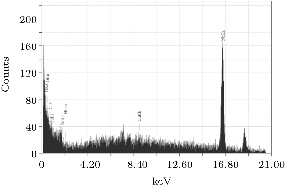 | Fig. 6. EDS spectrum of the film coated at 9 cm and 0° position with 30 plasma focus shots. |
A gradual decrease in nitrogen content in the coating is also observed for 10° and then 20° angular positions. In the plasma focus device, ions are emitted in a small solid angle along the anode axis and their flux decreases with increasing the angle, which results in the decrease of nitrogen content with increasing the angle.[56, 57] Figure 6 shows EDX spectra of the film coated at 9 cm and the 0° position.
An atomic force microscope (AFM) is employed to analyze the roughness of coated films at different axial and angular positions. Figures 7 and 8 represent two-dimensional topographies of the surfaces of film coatings synthesized at different axial and different angular positions respectively. A scan area of 5 μ m × 5μ m is selected to obtain all images.
 | Fig. 7. Atomic force micrographs of the coated films synthesized with 30 plasma focus shots at (a) 5 cm, (b) 9 cm, and (c) 13 cm along the anode axis. |
 | Fig. 8. AFM micrographs of samples exposed to 30 plasma focus shots at (a) 0° , (b) 10° , and (c) 20° angular positions at a 9-cm axial distance. |
The root-mean-square (RMS) roughness values of all film coatings are listed in Table 2. It is clear that the least value of RMS roughness is observed for film coating synthesized at the 9-cm axial distance as compared with at other (5 cm and 13 cm) distances. When the distance is increased from 9 cm to 13 cm, well separated larger size grains and clusters sparsely appear on the surface, resulting in rougher film than the relatively smooth film at 9 cm. Whereas at the 5-cm distance the extensive surface damages due to the influences of higher ion energy and flux result in a much coarser film than at the 9-cm distance.
The roughness values of films at 10° and 20° decrease gradually than at 0° , which is due to the non-uniform distribution of grains, caused by the lower energy flux of ions reaching at larger angular positions. Sohrabi et al.studied the angular distribution of nitrogen ions from a 4-kJ plasma focus device and reported the highest ion emission along the anode axis.[54]
| Table 2. RMS roughness values of film coatings at different axial and angular positions. |
The mechanical strength of film coatings is measured by employing a Wilson Wolpert 401MVA Vickers micro-hardness tester. Figure 9 shows the micro-hardness values (GPa) of the film coatings synthesized at zero degree angular position for different axial positions, each as a function of the applied load (gram force). The hardness of the virgin sample is also represented for comparison. The slow fall in the micro-hardness value with the increase of applied force is attributed to the formation of a thick compound layer because the increase in applied force simply causes the increase in indentation depth. The enhanced micro-hardness values for all samples are attributed to the deposition of niobium nitride/niobium oxy-nitride on the sample surface along with the interstitial implantation of nitrogen into niobium. The nitrogen ion bombardment creates the lattice distortion in niobium by their interstitial incorporation and creates point defects through induced collision cascades. This may enhance the micro-hardness values of film coatings. The maximum hardness of (8.44 ± 0.01) GPa is observed at the 5-cm axial position, which shows about a 500% increase in the hardness value of the untreated sample. The hardness decreases to (6.98 ± 0.01) GPa and then (1.86 ± 0.01) GPa when the film anode distance increases to 9 cm and then 13 cm. The maximum hardness at the 5-cm position may be due to the maximum nitrogen content in the coated film as compared with at the other axial positions, owing to the maximum ion energy and flux reached at this axial position, which is also confirmed by EDX analysis. The increasing nitrogen content results in the increase in the material hardness in principle.[58] EDX spectra show the decrease in nitrogen in film coatings with the increase of axial distance, which is probably responsible for the trend of micro-hardness decreasing with increasing the axial distance.
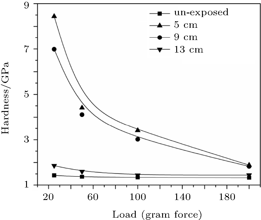 | Fig. 9. Variations of hardness of film coating with applied load for different axial positions along the anode axis for 30 plasma focus shots. |
Figure 10 demonstrates micro-hardness values of coated films at different angular positions for a 9-cm distance. The hardness is observed to decrease with increasing the angle with respect to the anode axis. A minimum hardness of about (1.55 ± 0.01) GPa is observed for 20° angle because of the oblique incidence of ions with relatively low flux at this angular position. It has been reported that in the plasma focus device, the nitrogen ion density significantly dropped for angles higher than ± 11° (with respect to the anode axis)[54] and most of the ions are emanated out of a pinched plasma column in a small solid angle along the anode axis and their flux decreases with increasing the angle.[57] So, lower nitrogen concentrations in coatings at 10° and 20° (also confirmed by EDX analysis) are responsible for lower hardness values of coating at these positions.
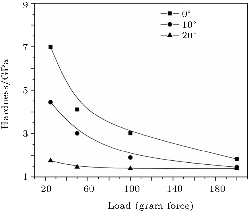 | Fig. 10. Variations of the hardness of film coatings with applied load for different angular positions at a 9-cm axial distance for 30 plasma focus shots. |
In this paper, the effect of deposition parameters on the synthesis of niobium nitride using a plasma focus device is studied. The synthesized coatings are analyzed by a multiple characterization technique. XRD confirms the growth of multi-phase NbN/Nb2N/NbO0.12N0.88 film coating. The downshifts in all diffraction peaks from the corresponding standard stress-free positions are observed at the 5-cm axial distance, which is attributed to residual stresses induced in the film caused by ion implantation. SEM shows the granular surface morphology with a strong thermally assisted coagulation effect observed at 5-cm axial distance, which is due to the higher ion energy flux. The non-porous granular morphology observed at 9-cm distance along the anode axis is different from those observed at 10° and 20° due to the attenuation of flux at the large angle. EDX spectra reveal a maximum nitrogen content at the shortest (5 cm) axial position. AFM exhibits that the roughness of coated films varies for coatings synthesized at different axial and angular positions. The maximum hardness value of (08.44 ± 0.01) GPa is achieved for the film coating achieved at a 5-cm axial distance which is about 500% higher than that of a virgin sample. Hardness is found to be reduced for higher axial positions due to the lower nitrogen (and oxygen) content in the coating at the larger distance. The hardness also decreases at the higher angle due to the flux attenuating with increasing the angle with respect to the anode axis.
The authors would like to thank Prof. Dr. Saadat Anwar Siddiqi and Ms. Tehseen Riaz, working at the Interdisciplinary Research Centre in Biomedical Materials (IRCBM), COMSATS Institute of Information Technology (CIIT), Lahore for their technical support in the Vickers hardness analysis. Ms. Uzma Ikhlaq and Mr. Rana Ayub are also acknowledged for technical support in XRD and AFM analysis respectively. One of the authors (Jamil Siddiqui) is grateful to the HEC for providing financial support during his PhD research work.
| 1 |
|
| 2 |
|
| 3 |
|
| 4 |
|
| 5 |
|
| 6 |
|
| 7 |
|
| 8 |
|
| 9 |
|
| 10 |
|
| 11 |
|
| 12 |
|
| 13 |
|
| 14 |
|
| 15 |
|
| 16 |
|
| 17 |
|
| 18 |
|
| 19 |
|
| 20 |
|
| 21 |
|
| 22 |
|
| 23 |
|
| 24 |
|
| 25 |
|
| 26 |
|
| 27 |
|
| 28 |
|
| 29 |
|
| 30 |
|
| 31 |
|
| 32 |
|
| 33 |
|
| 34 |
|
| 35 |
|
| 36 |
|
| 37 |
|
| 38 |
|
| 39 |
|
| 40 |
|
| 41 |
|
| 42 |
|
| 43 |
|
| 44 |
|
| 45 |
|
| 46 |
|
| 47 |
|
| 48 |
|
| 49 |
|
| 50 |
|
| 51 |
|
| 52 |
|
| 53 |
|
| 54 |
|
| 55 |
|
| 56 |
|
| 57 |
|
| 58 |
|