
Graded doping low internal loss 1060-nm InGaAs/AlGaAs quantum well semiconductor lasers*
[Tan Shao-Yang† , Zhai Teng, Zhang Rui-Kang, Lu Dan, Wang Wei, Ji Chen]
, Zhai Teng, Zhang Rui-Kang, Lu Dan, Wang Wei, Ji Chen]
|
|


†Corresponding author. E-mail: tanshy10@semi.ac.cn
*Project supported by the National Natural Science Foundation of China (Grant Nos. 61274046, 61335009, 61201103, and 61320106013) and the National High Technology Research and Development Program of China (Grant No. 2013AA014202).
Internal loss is a key internal parameter for high power 1060-nm InGaAs/AlGaAs semiconductor laser. In this paper, we discuss the origin of internal loss of 1060-nm InGaAs/GaAs quantum well (QW) AlGaAs separate confinement heterostructure semiconductor laser, and the method to reduce internal loss. By light doping the n-cladding layer, and stepwise doping the p-cladding layer combined with the expanded waveguide layer, a broad area laser with internal loss of 1/cm is designed and fabricated. Ridge waveguide laser with an output power of 350 mW is obtained. The threshold current and slope efficiency near the threshold current are 20 mA and 0.8 W/A, respectively.
High power semiconductor lasers are widely used as the pumping source for solid-state laser, [1– 4] seeding source in master oscillator power amplifier (MOPA) system, [5] and frequency-doubling applications[6] due to their high efficiency, high reliability, compact size, and low cost. High optical power provided by semiconductor laser is a key requirement to achieve higher output power[1– 5] and higher energy conversion efficiency in these applications.[5] The principle idea to increase the output power of a semiconductor laser is to increase the light-current slope efficiency and the power-current saturation current injection level. The main obstacle to the increase of power is the thermal roll-over effect caused by current-induced heating up of the active region. To suppress this effect, a long laser cavity is necessary to reduce the thermal and residue resistance, whereas, external quantum efficiency will drop off with the increase of cavity length, and the accumulated loss in the long cavity will become a major problem for high power applications. Accordingly, extremely low internal loss is of great importance for maintaining the external quantum efficiency and the slope efficiency.
The internal loss comes mainly from waveguide scattering loss[7– 9] and free carrier absorption.[10– 13] For GaAs-based separate confinement heterostructure (SCH) quantum well semiconductor laser with an emission wavelength of around 1 μ m, internal loss is attributed to free carrier absorption in QW-active layer, high doping cladding layer, and undoped waveguide layer to some extent.[8, 13] Therefore, by designing the doping profile of the cladding layer or extending the thickness of the waveguide layer, the internal loss can be reduced and an internal loss around 1/cm has been reported.[14– 16] But little work has focused on the influence of the doping profile of the cladding layer on the internal loss of high power 1060-nm InGaAs/GaAs double quantum well (DQW) AlGaAs SCH laser.
In this paper, we investigate the sources of internal optical loss in 1060-nm InGaAs/GaAs DQW AlGaAs heterostructure laser with grade doping cladding layers. The influences of doping profile and waveguide thickness on the internal loss of InGaAs/GaAs quantum well SCH laser are studied theoretically and experimentally. By introducing a step doping profile in the cladding layer combined with properly expanded waveguide, broad area laser with an internal loss of 1/cm is obtained. Furthermore, based on the low internal loss design, ridge waveguide laser with an output power of 350 mW, a threshold current of 20 mA, and slope efficiency near threshold current of 0.8 W/A are obtained.
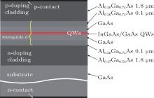
Figure 1 shows the separate confinement heterostructure (SCH) double quantum well semiconductor laser investigated in this paper. The structure consists of n- and p-doped cladding layers and undoped waveguide layers and QW layers. Here we define the thickness of the undoped region including the waveguide layer and QW layers as d. The internal loss of a QW SCH laser can be determined by[17]

in the transversal direction. P = ∫ | E(x)| 2 dx, E(x) is the one-dimensional electric-field distribution of fundamental TE mode in the transversal waveguide, is the material optical loss at position x, originating from free carrier absorption which depends linearly on the carrier density, [18] i.e., α = α fc = σ nn + σ pp, where n and p are the densities of electrons and holes respectively, σ n and σ p are the absorption cross sections of the electrons and holes respectively, which are determined experimentally.[13]
 | Fig. 1. Schematic structure of broad area laser under investigation in this paper. |
The carriers come from ionization of local dopants, diffusion from adjacent doped area and carrier injections. In a real high power device, only the lower and upper cladding layers are doped intentionally (Si for n-cladding layer and C-dope for p-cladding layer). Figure 2 shows the doping level of the real device, measured by second ion mass spectrum (SIMS), and carrier density distribution at room temperature when the LD device is forward biased at the laser threshold, which is calculated by commercial software Crosslight. As can be seen, carriers only concentrate at the n- and p-cladding layer and QW layer, while in the undoped waveguide layer the carrier concentration can be ignored. The free carrier concentration in cladding layers depends on the doping level. While for the QW layers, the densities of carriers, i.e., the densities of electrons and holes are both clamped at a threshold of around 1 × 10¹⁸/cm3∼ 2 × 10¹⁸/cm3.
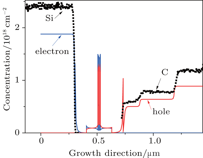 | Fig. 2. Calculated carrier distribution in the growth direction (solid line) and SIMS measured dopant concentration (dotted line). |
Thus, for a separate confinement heterostructure (SCH) quantum well semiconductor laser, the internal loss can be simplified into

where Γ QW is the optical confinement factor of QW layer; α QW is the material loss of quantum well from free carrier absorption; n(x) and p(x) are the doping profiles of n- and p-doped cladding layers, respectively.
According to the above relationship, the internal loss can be minimized by pushing the doped cladding layers far away from QW, which will reduce their optical confinement factor combined with light doping n-cladding layer and nonuniform doping p-cladding layer, namely the doping level increases at growth direction, which will reduce the overlap of carrier and optical mode and have no effect on electron leakage to cladding layer.
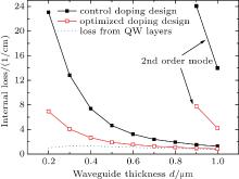
In our experiment, we reduce the internal loss by optimizing doping levels in the cladding layers and increasing the thickness values of waveguide layers. The doping of n- and p-cladding layers is optimized in different ways. For n-cladding layer, the doping level along growth direction is uniform and low, while for p-cladding layer doping increases stepwise as shown in Fig. 2. The doping concentration is 5 × 1017 cm− 3 near the edge of the waveguide layer, 7 × 1017 cm− 3 at the center, and 1 × 1018 cm− 3 near the top contact layer. The calculated relations between the internal loss and the thickness of the waveguide layer of different doping profiles are shown in Fig. 3. The absorption cross section coefficients of σ n = 6 × 10− 18 cm− 2 and σ p = 14 × 10− 18 cm− 2 are used.[13] By optimizing the doping profiles of cladding layers, internal loss is reduced dramatically from 23/cm to 7/cm in the case of a thin waveguide. When the thickness of the waveguide layer d is expanded up to 1 μ m, the total internal loss is reduced significantly. In this case, apart from the main part of internal loss coming from QW layers, the design with optimized doping profile providing lower internal loss is of great significance for low internal loss applications. Although a higher order transversal mode appears when waveguide thickness d > 0.9 μ m, it can be suppressed by its relatively high internal loss. As waveguide thickness extends from 0.2 μ m to 1 μ m, the QW optical confinement factor changes slightly from 0.023 to 0.019. The threshold gain and threshold current will be raised by less than 21%. The influence on laser performance can be ignored as high power laser diodes always work at high injection level with current several ten times higher than that of threshold condition. According to the calculation relationship, we design and fabricate a series of broad area lasers with different doping profiles and various waveguide layer thickness values. The detailed information about the design parameters is listed in Table 1.
The entire epitaxial structures of the lasers are grown with low pressure metal– organic chemical vapor deposition (LP-MOCVD). The structure consists of n-GaAs buffer and contact layer, 1.8-μ m n- and p-doping Al0.47Ga0.53As cladding layer, 100-nm un-doped Al0.26Ga0.74As step cladding layers, GaAs waveguide layers, and active layer. The growth temperature of AlGaAs cladding layers is elevated to 640 ° C in order to reduce the background carbon and oxide concentration. The n-cladding layers are Si-doped, with a doping level of 2.4 × 1018 cm− 3 and for p-cladding layer C is utilized to obtain the designed step doping profile. Two compressively strained InGaAs/GaAs quantum wells with gain peak around 1060 nm are employed in the active layer. The growth condition is optimized systematically to obtain high quality QWs.
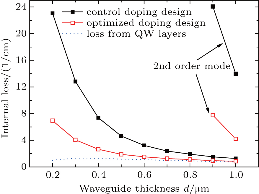 | Fig. 3. Calculated internal losses as a function of waveguide thickness d. |
| Table 1. Different structures of design. |
The post-growth proceeding of broad area lasers is as follows: P-side contact is performed by vacuum deposition of Ti/Au. The Ti/Au is patterned into 100-μ m wide stripe and the highly doped GaAs contact layer except that the Ti/Au metal pattern is wet-etched to provide carrier confinement. The wafer is lapped to 100 μ m in thickness, and backside Ohmic contact is made by AuGeNi/Au metallization after backside polishing. Laser bars of various cavity lengths ranging from 500 μ m to 4000 μ m are cleaved. Ridge waveguide laser are fabricated with the same procedures as those in our previous work.[19– 21] Ridge waveguide of 4.5 μ m is etched, then p-side and back-side Ohmic contact are performed. The rear and front facet are high and anti-reflectivity coated, with reflectivities of 99% and 9%, respectively. For continuous wave (CW) testing, lasers are soldered p-side up on Cu submounts and attached to a copper heatsink.
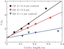
To extract the internal loss of the laser structures experimentally, pulse power current test is performed for BA lasers with various cavity lengths ranging from 500 μ m to 4000 μ m. The pulse width of 1 μ s and duty cycle of 0.5% are selected to avoid current-induced heating of the laser waveguide and active region. Figure 4 shows the plots of measured inverse differential quantum well efficiency (1//η d) as a function of cavity length for three designed structures. For each test data point, more than 10 identical BA lasers are tested, and the mean value is used. Figure 4 also shows the linear fit plot of the measurement data of four structures using the model

where η i is the internal quantum efficiency. The fitting results of internal quantum efficiency η i and internal loss α i for three design structures are shown in Table 1. The values of internal loss α i from the experiment match well with the theoretically calculated result, when considering the fact that the experimental error is in a range of ± 10%. By light doping the n-cladding layer, stepwise doping the p-cladding layer and expanding the GaAs waveguide layer by a factor of 5, the internal loss is reduced from 6.6/cm to 1.0 /cm. None of the internal quantum efficiencies of the three structures has an obvious reduction when expanding the waveguide layer, which indicates that the effect of the carriers escaped from QWs on the waveguide layer is insignificant in each of these structures.
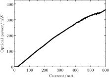
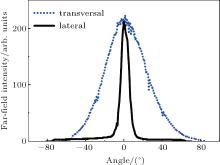
Figure 5 shows the CW power– current property of ridge waveguide laser with a cavity length of 1 mm at room temperature. The threshold current is less than 20 mA. Near the threshold condition, slope efficiency over 0.8 W/A is obtained from the front facet as a result of internal loss reduction. Owing to the thermal effect, the slope efficiency drops off slowly as injection current increases. The transversal and lateral far-field profile measured at 550 mA are shown in Fig. 6. The single lobe far-field profile in the vertical direction indicates that no higher order transversal mode is excited. The full width at half maximum (FWHM) angles are 50° and 10° in the vertical and lateral directions, respectively. The corresponding output power is 350 mW. With further increasing the injection current, PI kink and high order lateral mode emerge.
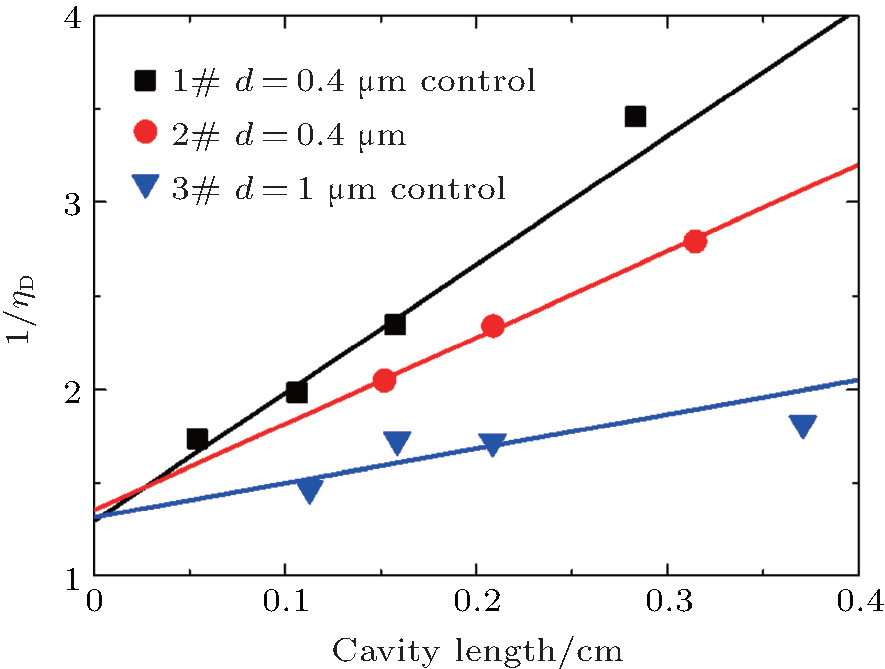 | Fig. 4. Plots of inverse external differential quantum efficiency 1/η d versus cavity length L. |
 | Fig. 5. The CW power– current property of ridge waveguide laser at room temperature. |
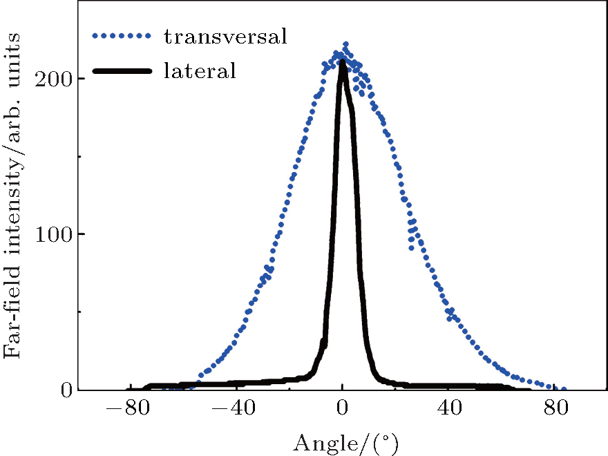 | Fig. 6. Transversal and lateral far-field profiles of the ridge waveguide laser at 550 mA at room temperature. |
Internal optical loss of 1060-nm InGaAs/GaAs QW AlGaAs separate confinement heterostructure semiconductor laser is studied in this paper. Our calculations indicate that the internal losses are due mainly to free carrier absorption of QW layers and cladding layers, while the contribution of the waveguide layer can be ignored. By light doping of the n-cladding layer and introducing stepwise doping of the p-cladding layer combined with expanding the waveguide layer, a broad area laser with relatively low internal loss of 1/cm is achieved. Based on the low internal loss structure, a ridge waveguide laser with a high single spatial mode output power of 350 mW is obtained. For further improvement, internal loss of the lasers can be reduced by further expanding the waveguide layer and optimizing the material composition of the waveguide.
| 1 |
|
| 2 |
|
| 3 |
|
| 4 |
|
| 5 |
|
| 6 |
|
| 7 |
|
| 8 |
|
| 9 |
|
| 10 |
|
| 11 |
|
| 12 |
|
| 13 |
|
| 14 |
|
| 15 |
|
| 16 |
|
| 17 |
|
| 18 |
|
| 19 |
|
| 20 |
|
| 21 |
|