


Achieving a multi-band metamaterial perfect absorber via a hexagonal ring dielectric resonator*
[Li Li-Yang, Wang Jun† , Du Hong-Liang, Wang Jia-Fu, Qu Shao-Bo‡]
, Du Hong-Liang, Wang Jia-Fu, Qu Shao-Bo‡]
|
|


†Corresponding author. E-mail: wangjun563@163.com
‡Corresponding author. E-mail: qushaobo@mail.xjtu.edu.cn
*Project supported by the National Natural Science Foundation of China (Grant Nos. 61331005, 11204378, 11274389, 11304393, and 61302023), the Aviation Science Foundation of China (Grant Nos. 20132796018 and 20123196015), the Natural Science Foundation for Post-Doctoral Scientists of China (Grant Nos. 2013M532131 and 2013M532221), the Natural Science Foundation of Shaanxi Province, China (Grant No. 2013JM6005), and the Special Funds for Authors of Annual Excellent Doctoral Degree Dissertations of China (Grant No. 201242).
A multi-band absorber composed of high-permittivity hexagonal ring dielectric resonators and a metallic ground plate is designed in the microwave band. Near-unity absorptions around 9.785 GHz, 11.525 GHz, and 12.37 GHz are observed for this metamaterial absorber. The dielectric hexagonal ring resonator is made of microwave ceramics with high permittivity and low loss. The mechanism for the near-unity absorption is investigated via the dielectric resonator theory. It is found that the absorption results from electric and magnetic resonances where enhanced electromagnetic fields are excited inside the dielectric resonator. In addition, the resonance modes of the hexagonal resonator are similar to those of standard rectangle resonators and can be used for analyzing hexagonal absorbers. Our work provides a new research method as well as a solid foundation for designing and analyzing dielectric metamaterial absorbers with complex shapes.
In 2008, Landy et al.[1] put forward a perfect absorber based on metallic structure metamaterial, which contains an electric resonator coupling with incident electric field and a magnetic resonator coupling with incident magnetic field. Owing to strong resonance of the metallic structure, the absorptivity can reach nearly unity. Afterward, the perfect metamaterial absorber became one of the focal fields, which aroused the interest of researchers all over the world. Metamaterial absorbers based on metallic patterns developed rapidly in recent years, from polarization-independent, [2] wide angle-of-incidence absorbers[3– 6] to multi-band, [6, 7] broadband absorbers, [8, 9] from microwave[1, 4, 6, 8] to terahertz, [2, 3, 7, 9] infrared [10– 13] and optical absorbers.[5, 14– 16]
The studies of perfect absorbers have achieved remarkable success in improving the absorbing performance. However, most of the above-mentioned metamaterial absorbers are based on metallic structures. The metallic structures have some advantages. Nevertheless, metallic structures are prone to be oxidized and corroded under high temperatures. Alternatively, dielectrics can make up these deficiencies and are advantageous in high-power and high-temperature applications, so it is meaningful to investigate dielectric absorber design. In recent years, remarkable progress has been achieved for dielectric metamaterials in theory, [17– 22] experiments, [17, 23– 25] and applications.[26– 28] This provides a good foundation for the study of dielectric absorbers. However, at present, few relevant studies are reported, giving no applicable examples. In 2013, Liu et al.[29] proposed a perfect absorber via high-permittivity dielectric cubes on metal plates, and the effects on absorption were studied by changing the edge length and the permittivity of the dielectric material. The absorber achieves single frequency absorption in X-band.
In this paper, a multi-band dielectric perfect absorber in microwave regime is proposed. A hexagonal ring structure made of high-permittivity dielectrics is employed to fabricate the absorber. Considering the fact that Mie scattering theory[29] and dielectric resonator theory[22] are essentially equivalent in revealing resonant modes of high permittivity dielectrics, the dielectric resonator theory (which is more convenient especially for resonators with complex shapes and boundaries) is used to analyze the multi-band perfect absorption. It is found that the resonant modes of the complex hexagonal structure are similar to those of standard rectangle resonators. This approximate methodology provides new ideas and methods for future studies on dielectric metamaterial absorbers with complex structures.
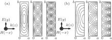
The dielectric hexagonal ring structure is shown in Fig. 1. The structure is made of SrTiO3 (the relative permittivity is 300 and the loss tangent is 0.005). As shown schematically in Fig. 1(a), the inner side length of the hexagonal ring is 2.5 mm and the height of the hexagonal ring is 1.0 mm. The thickness values for the two upper walls and the two lower walls are all 0.433 mm, while the two vertical walls are both 0.2165-mm thick. The hexagonal ring is placed on a copper backing plate and the unit cell is 14 mm× 14 mm in area as shown in Fig. 1(b).
 | Fig. 1. Description of the dielectric metamaterial absorber: (a) the hexagonal ring structure with geometrical parameters; (b) unit cell and periodic structures. |
The absorptivity of an absorber can be calculated from the transmission (T) and reflection (R), and is given by the following formula:

This absorber adopts a metal backing plate, so the transmission T is 0.
The commercial software CST MICROWAVE STUDIO 2011 is used for this simulation. A full-wave simulation based on the frequency domain solver is implemented in 9.0 GHz– 14.0 GHz. As shown in Fig. 2, the hexagonal ring structure has three resonant dips below – 10 dB in 9.0 GHz– 14.0 GHz. The three resonant dips are at 9.785 GHz, 11.525 GHz, 12.37 GHz, respectively. The corresponding reflections are -15.057 dB, -12.446 dB, and -25.94 dB, corresponding to absorptions about 96.88% , 94.31% , and 99.75% , respectively.
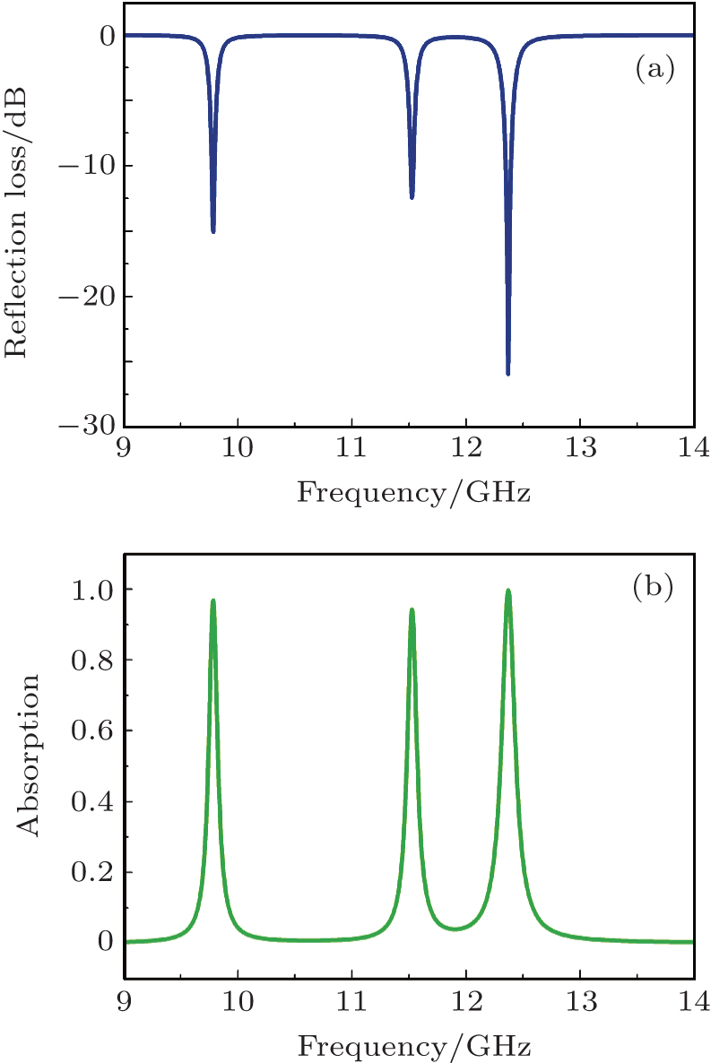 | Fig. 2. Reflection (a) and absorption (b) properties for the absorber. |
The electromagnetic responses at each absorption peak are analyzed to reveal the mechanism of the multi-band perfect absorption. We illustrate the main distribution features of electric and magnetic fields, and point out the mechanism of the perfect absorption.
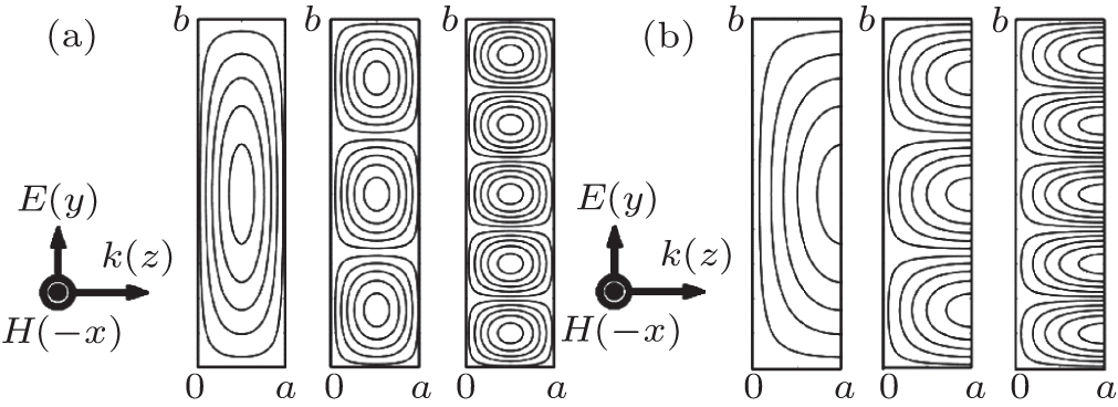
The hexagonal high-permittivity inclusions are treated as dielectric resonators. The resonance modes are analyzed based on the dielectric resonator theory. Analysis of a rectangular dielectric resonator is conducted using the method of mixed magnetic wall. This is helpful in providing the inner field distributions and the formula for calculating resonant modes under different boundary conditions.[21, 22] Take 
 | Fig. 3. Electric distributions for  |
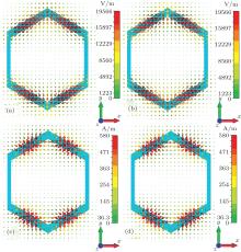
We first analyze the field distribution features at the first resonant frequency 9.785 GHz. The reflection dip is -15.057 dB, with absorption about 96.88% . As shown in Fig. 4, electromagnetic fields inside the hexagonal ring are focused on the two upper walls and the two lower walls, while there is almost no field in the two vertical walls. Figure 4 shows the electric and magnetic field distributions on x– y plane at 9.785 GHz. As shown in Fig. 4, the electric fields inside the upper and lower walls resonate along the walls back and forth. In order to describe the resonance process in detail, we monitor the field distributions at different excitation phases (the phase on the plane where the incident port lies). The electric field resonances are stronger when the excitation phases are 135° and 315° than when at the other phases. In addition, the magnetic fields in the walls are vertical to the electric fields. The magnetic field distribution can be regarded as a magnetic dipole. The magnetic field is more intense when the excitation phases are 45° and 225° .
 | Fig. 4. Electric and magnetic fields at 9.785 GHz. (a) Electric field distribution in x– o– y plane for the excitation phase is 135° . (b) Electric field distribution in x– o– y plane for the excitation phase of 315° . (c) Magnetic field distribution in x– o– y plane for the excitation phase of 45° . (d) Magnetic field distribution in x– o– y plane for the excitation phase of 225° . |
Figure 5 shows the electric fields of the four upper/lower sides further simulated by Matlab programming. Denote x– o– y plane by plane A and the inner ring side by plane B. In Fig. 5, the bottom surface of the hexagonal ring contacts the copper plate. Thus, the bottom surface can be treated as the electric wall. The electric fields are perpendicular to the electric wall. The top surface of the hexagonal ring can be considered as a magnetic wall, on which the electric field is tangential. Therefore, semicircular electric field lines are formed on plane B. Due to the mirror effect of the copper plate, equivalent closed loops of electric field lines are formed on the four upper/lower sides. The electric field component perpendicular to the loops remains zero. The resonant mode can be seen as TE mode. Using Ploss ∝ | Eloc| 2(1 − e− 2α x) (where α represents the attenuation coefficient, x represents the thickness of the absorber), we can see that the power loss is proportional to the squared localized field intensity in the dielectric resonator. It is the resonance that leads to intensified fields and thus a strong absorption effect.
 | Fig. 5. Electric field simulation for the four upper/lower sides. |
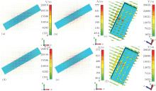
A simple analogy between the four upper/lower sides and standard rectangular dielectric resonators is carried out to clarify the resonant modes. As shown in Fig. 6, the standard rectangular resonator has basically the same sizes of the four upper/lower sides. The geometrical dimensions of the rectangular resonator are 2.5 mm× 0.433 mm× 1.0 mm with a tilted angle of 30° with respect to x direction. The resonant mode of the standard rectangular resonator is similar to those of the four upper/lower sides of the hexagonal ring dielectric resonator.
 | Fig. 6. Standard rectangular resonator extracted from the hexagonal dielectric resonator. |
As shown in Fig. 7, the magnetic field and the electric field of the rectangular resonator are similar to those of the four upper/lower hexagonal ring sides at the resonant frequency. Figures 7(a) and 7(d) show the electric field distributions in plane A for the excitation phases of 135° and 315° respectively. The electric field distribution is almost the same as that of the hexagonal ring. Figures 7(b) and 7(e) show the magnetic field distributions in plane A for the excitation phases of 45° and 225° respectively. The magnetic fields are perpendicular to the electric fields, equivalent to a magnetic dipole. This resonant mode is TE mode. Figures 7(c) and 7(f) show the electric field distributions in plane B for the excitation phases of 135° and 315° respectively. It can be shown that the electric field lines are also in the shape of a semicircle, similar to those in Fig. 5.
 | Fig. 7. Electric and magnetic field distributions for the rectangular resonator. (a) Electric field distribution in the x– o– y plane for the excitation phase of 135° . (b) Magnetic field distribution in the x– o– y plane for the excitation phase of 45° . (c) Electric field distribution in plane B for the excitation phase of 135° . (d) Electric field distribution in the x– o– y plane for the excitation phase of 315° . (e) Magnetic field distribution in the x– o– y plane for the excitation phase of 225° . (f) Electric field distribution in plane B for the excitation phase of 315° . |
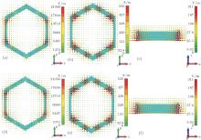
The second resonant frequency is located at 11.525 GHz. The reflection dip is -12.446 dB, with absorption about 94.31% . As shown in Fig. 8, strong electromagnetic responses are excited in all the six sides of the hexagon ring. Figures 8(a) and 8(d) show electric field distributions in the x– o– y plane for the excitation phases of 0° and 180° respectively. Electric fields on the two vertical sides resonate in the y direction. In this case, each vertical side is equivalent to an electric dipole. Figures 8(b) and 8(e) show magnetic field distributions in the x– o– y plane for the excitation phases of 90° and 270° respectively. The magnetic field is perpendicular to the electric field vector. For each of the four upper/lower sides, the magnetic fields form two loops in the x– o– y plane, which are opposite in direction. In this magnetic resonant response, the magnetic fields vanish in the z direction (Hz = 0), while none of the electric fields in the x, y, and z directions is zero. Thus the corresponding resonance mode is TM mode. On each vertical side, the magnetic fields form one loop in the x– o– z plane. The magnetic field in the y direction is zero (Hy = 0) as shown in Figs. 8(c) and 8(f), indicating that the resonant mode on the vertical side is TM mode. Figure 8(c) shows that the magnetic field forms an asymmetric ring, leading to a composite magnetic field in the positive x direction for the excitation phase of 90° . Similarly, the composite magnetic field direction is along the negative x direction for the excitation phase of 270° as shown in Fig. 8(f). From Ploss ∝ | Eloc| 2(1 − e− 2α x), we can see that the power loss is proportional to the squared field intensity. It is also the TM mode resonance on the six sides that leads to the enhanced localization field and produces a perfect absorption at the resonant frequency.
 | Fig. 8. Electric and magnetic field distributions at 11.525 GHZ. (a) Electric field distribution in the x– o– y plane for the excitation phase of 0° . (b) Magnetic field distribution in the x– o– y plane for the excitation phase of 90° . (c) Magnetic field distribution in the x– o– z plane for the excitation phase of 90° . (d) Electric field distribution in the x– o– y plane for the excitation phase of 180° . (e) Magnetic field distribution in the x– o– y plane for the excitation phase of 270° . (f) Magnetic field distribution in the x– o– z plane for the excitation phase of 270° . |
The third resonant frequency is located at 12.37 GHz, with a dip of -25.94 dB. The absorption is about 99.75% . As shown in Fig. 9, a strong electromagnetic response happens on all six sides of the hexagonal ring resonator, and the response is more intense on the two vertical sides. Figures 9(a) and 9(d) show the electric field distributions in the x– o– y plane when the excitation phases are 0° and 180° , when the electric fields reach their highest intensities. Each of the electric fields on the vertical sides resonates in the y direction, leading to an electric dipole. Figures 9(b) and 9(e) show the magnetic field distributions in the x– o– y plane when the excitation phases are 90° and 270° respectively. The magnetic field vector is perpendicular to the electric field vector. For each of the four upper/lower sides, the magnetic fields form three loops in the x– o– y plane, which are opposite in direction alternatively one by one. In this case, the magnetic fields are zero in the z direction (Hz = 0), while none of the electric fields in the x, y, and z directions is zero. Thus the corresponding resonance mode is TM mode. For the vertical sides, the magnetic fields form one loop in the x– o– z plane. The magnetic fields in the y direction are all zero (Hy = 0) as shown in Figs. 9(c) and 9(f), indicating that the resonant modes on the vertical sides are all TM mode. Figure 9(c) shows that the magnetic fields form an asymmetric ring, leading to a composite magnetic field in the positive x direction when the excitation phase is 90° . Similarly, the composite magnetic field direction is along the negative x direction when the excitation phase is 270° as shown in Fig. 9(f). The power loss is proportional to squared field intensity. It is the TM resonant modes on the four upper/lower sides and the two vertical sides that lead to enhanced field intensity. This produces a perfect absorption at the resonant frequency.
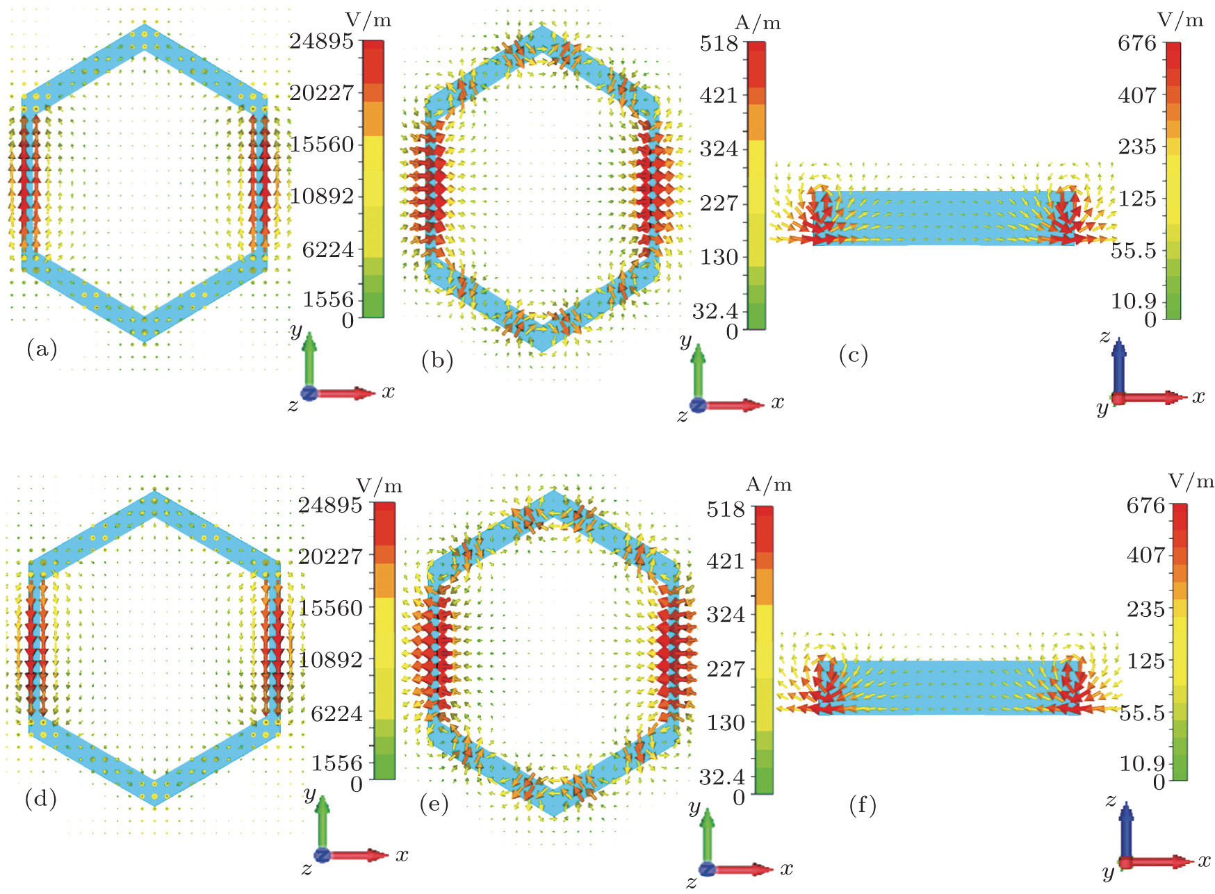 | Fig. 9. Electric and magnetic field distributions at 12.37 GHZ. (a) Electric field distribution in the x– o– y plane for the excitation phase of 0° . (b) Magnetic field distribution in the x– o– y plane for the excitation phase of 90° . (c) Magnetic field distribution in the x– o– z plane for the excitation phase of 90° . (d) Electric field distribution in the x– o– y plane for the excitation phase of 180° . (e) Magnetic field distribution in the x– o– y plane for the excitation phase of 270° . (f) Magnetic field distribution in the x– o– z plane for the excitation phase of 270° . |
The multi-band perfect absorption is investigated by analyzing the electric and magnetic field distributions at each absorption peak frequency. It is shown that the multi-band perfect absorptions originate from the enhanced field intensity. The enhanced localized fields, which are excited in the high dielectric resonators, lead to the enhanced absorption loss for incident waves.
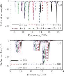
We investigate the variation of absorption peaks with the whole size of the dielectric resonator, the metal backing plate, and the dielectric permittivity. We set the scale of the original absorber as S = 1, then the scale factor varies from 0.7 to 1.2 (under ɛ = 300). Then, we change the dielectric permittivity from 285 to 315 (under S = 1). It can be seen from Fig. 10 that if we change the size or permittivity of the dielectric resonator, the absorption peak of the absorber will change, which is in good agreement with theoretical predictions. Figure 10(a) shows that the simulated absorption peak frequency decreases as the whole size of the absorber increases from 0.7 to 1.2 (under ɛ = 300). Figure 10(b) indicates that the absorption peak frequency decreases as the ɛ increases from 285 to 315 (under S = 1).
 | Fig. 10. Absorption properties for absorbers with different geometrical scales (a) and permittivies (b). |
In this paper, a multi-band absorber in the microwave regime is proposed using a hexagonal ring dielectric resonator. Unlike the metallic pattern-based absorbers, this absorber is composed of dielectric resonators and a metallic ground plate. Such an absorber is superior in inoxidizability, anticorrosion, and high-temperature resistance and high-power absorption, compared with their metallic counterpart. The mechanism for the near-unity absorption is caused by the electric and magnetic resonances where enhanced localized fields are excited in the dielectric resonator. In addition, the research offers an analogical method of simplifying a complex geometrical dielectric resonator into an equivalent simple dielectric resonator with similar resonance modes. By analyzing its resonant modes and adjusting resonant frequencies, broadband dielectric perfect absorbers can be achieved.
| 1 |
|
| 2 |
|
| 3 |
|
| 4 |
|
| 5 |
|
| 6 |
|
| 7 |
|
| 8 |
|
| 9 |
|
| 10 |
|
| 11 |
|
| 12 |
|
| 13 |
|
| 14 |
|
| 15 |
|
| 16 |
|
| 17 |
|
| 18 |
|
| 19 |
|
| 20 |
|
| 21 |
|
| 22 |
|
| 23 |
|
| 24 |
|
| 25 |
|
| 26 |
|
| 27 |
|
| 28 |
|
| 29 |
|